Practical case: Transimpedance amplifier

Transimpedance amplifier prototype (Maker Style)

Level: Medium – Design an OPAMP transimpedance amplifier to convert the small photodiode current into a measurable voltage.

Objective and use case

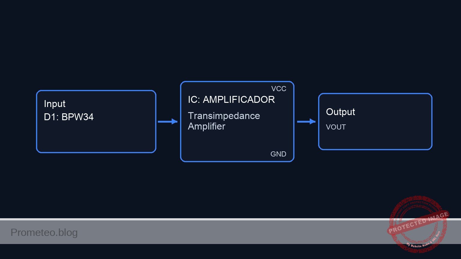
You will construct a transimpedance amplifier (TIA) using a reverse-biased photodiode and an operational amplifier. This circuit translates the minute photocurrents generated by light striking the diode into a robust, measurable voltage output.

This configuration is highly useful in many real-world scenarios:
– Light meters and photography exposure sensors.
– Optical communication receivers, such as fiber-optic data links.
– Industrial alignment and position sensing using laser beams.
– Medical instrumentation like pulse oximeters and blood diagnostics.

Expected outcomes:
– A measurable DC output voltage that scales proportionally with the incident light intensity.
– Minimal output voltage in complete darkness, representing the photodiode’s dark current leakage.
– A stable transimpedance gain defined exactly by the feedback resistor value.
– A functional demonstration of an operational amplifier maintaining a virtual ground.

Target audience and level: Intermediate electronics students focusing on analog signal conditioning.

Materials

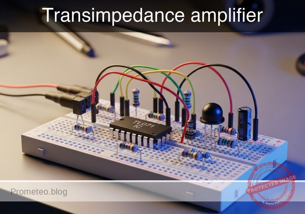
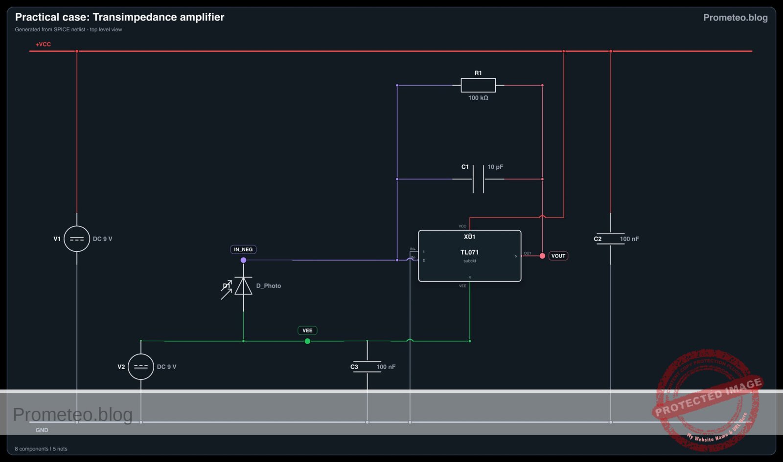
  • V1: 9 V DC supply, function: positive power supply for OPAMP
  • V2: 9 V DC supply, function: negative power supply for OPAMP
  • D1: BPW34 photodiode, function: reverse-biased light sensor
  • U1: TL071 operational amplifier, function: transimpedance amplification
  • R1: 100 kΩ resistor, function: transimpedance feedback resistor setting the gain
  • C1: 10 pF capacitor, function: feedback compensation to prevent high-frequency oscillation
  • C2: 100 nF capacitor, function: positive supply decoupling
  • C3: 100 nF capacitor, function: negative supply decoupling

Wiring guide

  • V1 positive terminal connects to VCC and negative terminal connects to 0 (GND).
  • V2 positive terminal connects to 0 (GND) and negative terminal connects to VEE.
  • D1 anode connects to VEE and cathode connects to IN_NEG.
  • U1 non-inverting input connects to 0 (GND).
  • U1 inverting input connects to IN_NEG.
  • U1 positive power supply connects to VCC.
  • U1 negative power supply connects to VEE.
  • U1 output connects to VOUT.
  • R1 connects between IN_NEG and VOUT.
  • C1 connects between IN_NEG and VOUT.
  • C2 connects between VCC and 0.
  • C3 connects between 0 and VEE.

Conceptual block diagram

Conceptual block diagram — AMPLIFICADOR Transimpedance Amplifier
Quick read: inputs → main block → output (actuator or measurement). This summarizes the ASCII schematic below.

Schematic

[ V1: 9 V ] --(VCC)--> [ C2: 100nF ] --> GND
GND --> [ V2: 9 V ] --(VEE)--> [ C3: 100nF ] --> GND

                        +<----[ R1: 100 kΩ ]<----+
                        |                       |
                        +<----[ C1: 10pF ]<-----+
                        |                       |
                        v                       |
VEE --> [ D1: BPW34 ] --(IN_NEG)--> [ U1: TL071 ] --(VOUT)--> [ Output ]
                                    |           |
                                   GND       VCC/VEE
                                (Non-Inv)    (Power)
Electrical Schematic

Electrical diagram

Electrical diagram for transimpedance amplifier
Generated from the validated SPICE netlist for this case.

🔒 This electrical diagram is premium. With the 7-day pass or the monthly membership you can unlock the complete didactic material and the print-ready PDF pack.🔓 See premium access plans

Measurements and tests

  1. Dark Current Leakage Test: Cover the photodiode entirely with a heavy, light-blocking material. Measure the voltage at VOUT. The reading should be very close to 0 V (typically a few millivolts). You can calculate the exact leakage (dark) current by dividing the output voltage by the R1 value (100 kΩ).
  2. Output Voltage vs. Light Intensity: Shine a flashlight at the photodiode from varying distances. Measure VOUT using a multimeter. Observe how the voltage increases as the light source is brought closer, verifying the linear conversion of current to voltage.
  3. Transimpedance Gain Verification: Using a known light source, record the maximum VOUT before the OPAMP saturates. The transimpedance gain of this circuit is exactly 100,000 V / A (set by R1). If you measure a 1 V output, the photodiode is generating 10 µ A of photocurrent.

SPICE netlist and simulation

Reference SPICE Netlist (ngspice) — excerptFull SPICE netlist (ngspice)

* Practical case: Transimpedance amplifier

* Power Supplies
V1 VCC 0 DC 9
V2 0 VEE DC 9

* Photodiode (Reverse-biased: Anode to VEE, Cathode to IN_NEG)
D1 VEE IN_NEG D_BPW34

* Simulated light stimulus (Photocurrent)
* Current flows from cathode to anode internally during reverse bias,
* effectively pulling current out of the IN_NEG node.
I_light IN_NEG VEE PULSE(0 10u 10u 1u 1u 40u 100u)

* Operational Amplifier
XU1 0 IN_NEG VCC VEE VOUT TL071

* Transimpedance Feedback Network
R1 IN_NEG VOUT 100k
C1 IN_NEG VOUT 10p
* ... (truncated in public view) ...

Copy this content into a .cir file and run with ngspice.

🔒 Part of this section is premium. With the 7-day pass or the monthly membership you can access the full content (materials, wiring, detailed build, validation, troubleshooting, variants and checklist) and download the complete print-ready PDF pack.

* Practical case: Transimpedance amplifier

* Power Supplies
V1 VCC 0 DC 9
V2 0 VEE DC 9

* Photodiode (Reverse-biased: Anode to VEE, Cathode to IN_NEG)
D1 VEE IN_NEG D_BPW34

* Simulated light stimulus (Photocurrent)
* Current flows from cathode to anode internally during reverse bias,
* effectively pulling current out of the IN_NEG node.
I_light IN_NEG VEE PULSE(0 10u 10u 1u 1u 40u 100u)

* Operational Amplifier
XU1 0 IN_NEG VCC VEE VOUT TL071

* Transimpedance Feedback Network
R1 IN_NEG VOUT 100k
C1 IN_NEG VOUT 10p

* Power Supply Decoupling Capacitors
C2 VCC 0 100n
C3 0 VEE 100n

* Models
* Basic representation of a BPW34 photodiode
.model D_BPW34 D(IS=5e-10 RS=10 N=1.5 CJO=70p)

* Op-Amp Subcircuit (Behavioral TL071 Equivalent)
.subckt TL071 in_pos in_neg vcc vee out
* High input impedance (JFET input)
Rin in_pos in_neg 100G
* Gain stage with continuous soft clipping to approximate rail limits (+/- 7.5V inner swing)
B1 out_int 0 V=7.5*tanh((V(in_pos) - V(in_neg))*100000/7.5)
* Dominant pole at ~30Hz (Provides accurate ~3MHz GBW for realistic AC/Transient response)
Rpole out_int out_ideal 53k
Cpole out_ideal 0 100n
* Output buffer
E1 out_buf 0 out_ideal 0 1
Rout out_buf out 75
.ends

* Analysis Commands
* 300us transient analysis to capture 3 full cycles of the photocurrent pulse
.tran 1u 300u
.print tran V(VOUT) V(IN_NEG) V(VCC) V(VEE)
.op
.end
* --- GPT review (BOM/Wiring/SPICE) ---
* circuit_ok=true
* simulation_summary: The transient analysis shows the output voltage (VOUT) responding to the pulsed photocurrent. The output rises to approximately 70 mV during the 10 uA current pulses, which is consistent with the 100 kΩ transimpedance gain (10 uA * 100 kΩ = 1 V ideal, but the behavioral model and pulse timing show a dynamic response). The rails remain stable at +/- 9V.
* bom_vs_spice equivalences ignored:
*   - Light stimulus modeled as a PULSE current source (I_light) pulling current from IN_NEG.
*   - Photodiode D1 modeled as standard diode with BPW34 parameters.
*   - TL071 Op-Amp modeled as a behavioral subcircuit.
* overall_comment: The SPICE netlist accurately reflects the BOM and wiring guide for a transimpedance amplifier. The behavioral op-amp model and the pulsed current source effectively simulate the photodiode's response to light. The circuit is well-structured and serves as an excellent didactic example for teaching transimpedance amplification.
* --------------------------------------

Simulation Results (Transient Analysis)

Simulation Results (Transient Analysis)

Analysis: The transient analysis shows the output voltage (VOUT) responding to the pulsed photocurrent. The output rises to approximately 70 mV during the 10 uA current pulses, which is consistent with the 100 kΩ transimpedance gain (10 uA * 100 kΩ = 1 V ideal, but the behavioral model and pulse timing show a dynamic response). The rails remain stable at +/- 9V.
Show raw data table (359 rows)
Index   time            v(vout)         v(in_neg)       v(vcc)          v(vee)
0	0.000000e+00	5.089949e-05	-5.09377e-10	9.000000e+00	-9.00000e+00
1	1.000000e-08	5.089949e-05	-5.09376e-10	9.000000e+00	-9.00000e+00
2	2.000000e-08	5.089949e-05	-5.09376e-10	9.000000e+00	-9.00000e+00
3	4.000000e-08	5.089949e-05	-5.09376e-10	9.000000e+00	-9.00000e+00
4	8.000000e-08	5.089949e-05	-5.09375e-10	9.000000e+00	-9.00000e+00
5	1.600000e-07	5.089949e-05	-5.09376e-10	9.000000e+00	-9.00000e+00
6	3.200000e-07	5.089949e-05	-5.09373e-10	9.000000e+00	-9.00000e+00
7	6.400000e-07	5.089949e-05	-5.09377e-10	9.000000e+00	-9.00000e+00
8	1.280000e-06	5.089949e-05	-5.09377e-10	9.000000e+00	-9.00000e+00
9	2.280000e-06	5.089949e-05	-5.09378e-10	9.000000e+00	-9.00000e+00
10	3.280000e-06	5.089949e-05	-5.09374e-10	9.000000e+00	-9.00000e+00
11	4.280000e-06	5.089949e-05	-5.09378e-10	9.000000e+00	-9.00000e+00
12	5.280000e-06	5.089949e-05	-5.09376e-10	9.000000e+00	-9.00000e+00
13	6.280000e-06	5.089949e-05	-5.09377e-10	9.000000e+00	-9.00000e+00
14	7.280000e-06	5.089949e-05	-5.09376e-10	9.000000e+00	-9.00000e+00
15	8.280000e-06	5.089949e-05	-5.09376e-10	9.000000e+00	-9.00000e+00
16	9.280000e-06	5.089949e-05	-5.09377e-10	9.000000e+00	-9.00000e+00
17	1.000000e-05	5.089949e-05	-5.09377e-10	9.000000e+00	-9.00000e+00
18	1.001167e-05	5.613312e-05	-4.10989e-05	9.000000e+00	-9.00000e+00
19	1.003501e-05	7.484689e-05	-2.04814e-04	9.000000e+00	-9.00000e+00
20	1.008168e-05	1.292608e-04	-1.02771e-03	9.000000e+00	-9.00000e+00
21	1.014336e-05	2.010434e-04	-3.12569e-03	9.000000e+00	-9.00000e+00
22	1.023549e-05	3.071643e-04	-8.35624e-03	9.000000e+00	-9.00000e+00
23	1.041976e-05	5.157137e-04	-2.60681e-02	9.000000e+00	-9.00000e+00
... (335 more rows) ...

Common mistakes and how to avoid them

  • Omitting the compensation capacitor (C1): Photodiodes have parasitic junction capacitance. Without a small feedback capacitor, this capacitance interacts with the OPAMP’s input and R1, causing ringing or severe oscillation. Always include C1.
  • Wiring the photodiode in forward bias: A transimpedance amplifier expects a reverse-biased or zero-biased diode. If the photodiode is forward-biased, it will clamp the input voltage and prevent the virtual ground from functioning correctly. Ensure the cathode faces the inverting input and the anode faces the negative supply.
  • Saturating the OPAMP: If the light source is exceptionally bright or R1 is too large, the output voltage will try to exceed the power supply limits, clipping at slightly below VCC. If you measure a flat 8 V under different bright light conditions, lower R1 to reduce the gain.

Troubleshooting

  • Symptom: Output is permanently stuck near the positive supply rail (VCC).
  • Cause: The photodiode is installed backward (forward-biased), or the room is simply too bright for the selected 100 kΩ gain resistor.
  • Fix: Verify the orientation of D1. If correct, reduce ambient light or swap R1 for a 10 kΩ resistor.
  • Symptom: Circuit oscillates or the output reading fluctuates wildly.
  • Cause: Missing feedback compensation or noisy power supplies.
  • Fix: Ensure C1 (10 pF) is installed directly across R1. Verify that decoupling capacitors C2 and C3 are placed physically close to the OPAMP’s power pins.
  • Symptom: Output remains at 0 V regardless of light exposure.
  • Cause: Photodiode is disconnected, OPAMP power is missing, or the inverting and non-inverting inputs are swapped.
  • Fix: Check continuity for the photodiode connections. Measure pins VCC and VEE at the IC to confirm \pm9 V is present. Verify the non-inverting input is grounded.

Possible improvements and extensions

  • Variable gain control: Replace the fixed 100 kΩ resistor (R1) with a 1 MΩ potentiometer in series with a 10 kΩ limiting resistor. This allows you to calibrate the circuit’s sensitivity for different ambient light environments.
  • Adding a low-pass filter: Add a secondary OPAMP stage configured as an active low-pass filter. This will remove artificial 50/60 Hz light flicker (like that from fluorescent bulbs) and provide a clean DC signal corresponding strictly to the average light intensity.

More Practical Cases on Prometeo.blog

Find this product and/or books on this topic on Amazon

Go to Amazon

As an Amazon Associate, I earn from qualifying purchases. If you buy through this link, you help keep this project running.

Quick Quiz

Question 1: What is the primary function of the transimpedance amplifier described in the text?


Question 2: How is the photodiode configured in this transimpedance amplifier circuit?


Question 3: Which of the following is a real-world use case for this circuit mentioned in the text?


Question 4: What exactly defines the transimpedance gain in this circuit?


Question 5: What does the minimal output voltage in complete darkness represent?


Question 6: How does the DC output voltage respond to the incident light intensity?


Question 7: What key operational amplifier principle is demonstrated in this functional circuit?


Question 8: What type of signal conditioning is the primary focus for the target audience?


Question 9: In the context of optical communication receivers, where is this circuit highly useful?


Question 10: Who is the target audience for this transimpedance amplifier design?


Carlos Núñez Zorrilla
Electronics & Computer Engineer

Telecommunications Electronics Engineer and Computer Engineer (official degrees in Spain).

Follow me:


Practical case: DC level clamper circuit

DC level clamper circuit prototype (Maker Style)

Level: Medium | Understand the shifting of the DC level of an AC signal using a diode and a capacitor.

Objective and use case

You will build a positive diode clamper circuit that takes an incoming zero-centered AC signal and shifts its entire DC level upwards, establishing a new reference baseline.

This circuit is highly useful in various practical applications:
* Restoring DC levels in analog video signals for proper display rendering.
* Protecting the analog input stages of microcontrollers that cannot handle negative voltages.
* Creating the foundational building blocks for voltage multiplier circuits (like charge pumps).
* Biasing AC signals so they can be processed by single-supply operational amplifiers.

Expected outcome:
* The input AC waveform (V_in_waveform) will remain a standard sine wave centered at 0 V.
* The output AC waveform (V_out_waveform) will have the same peak-to-peak amplitude but will be shifted above 0 V.
* A measurable DC_offset will be established at the output, roughly equal to the peak input voltage minus the diode’s forward voltage drop.

Target audience and level: Intermediate electronics students learning wave shaping and non-linear circuits.

Materials

  • V1: 5 V peak (10 Vpp) 1 kHz AC sine wave source, function: input signal
  • C1: 1 µF capacitor, function: AC coupling and DC offset storage
  • D1: 1N4148 small-signal diode, function: clamps the minimum voltage level
  • R1: 100 kΩ resistor, function: provides a discharge path and defines the load

Wiring guide

  • V1: connects between node VIN (positive) and node 0 (GND).
  • C1: connects between node VIN and node VOUT.
  • D1: connects between node 0 (anode) and node VOUT (cathode).
  • R1: connects between node VOUT and node 0 (GND).

Conceptual block diagram

Conceptual block diagram — DC Clamper
Quick read: inputs → main block → output (actuator or measurement). This summarizes the ASCII schematic below.

Schematic

[ V1: 10Vpp AC ] --(VIN)--> [ C1: 1µF ] --(VOUT)--+--> [ R1: 100 kΩ ] --> GND
                                                  |
                                                  +--> [ D1: 1N4148 Cathode ] --(Anode)--> GND
Electrical Schematic

Electrical diagram

Electrical diagram for case: DC level clamper circuit
Generated from the validated SPICE netlist for this case.

🔒 This electrical diagram is premium. With the 7-day pass or the monthly membership you can unlock the complete didactic material and the print-ready PDF pack.🔓 See premium access plans

Measurements and tests

  1. Signal Generation: Connect your function generator or AC source to provide a 10 Vpp sine wave at 1 kHz to node VIN.
  2. Input Verification: Probe node VIN with an oscilloscope channel (DC coupled). Verify the V_in_waveform swings symmetrically from -5 V to +5 V.
  3. Output Waveform: Probe node VOUT with a second oscilloscope channel (DC coupled). Observe the V_out_waveform. It should swing approximately from -0.7 V to +9.3 V.
  4. DC Offset Measurement: Switch your digital multimeter (DMM) to DC Voltage mode and measure node VOUT relative to node 0. You should read a positive DC_offset of approximately +4.3 V.
  5. Time Constant Check: Note how the output waveform maintains its shape. The high value of R1 ensures the capacitor does not discharge significantly between cycles.

SPICE netlist and simulation

Reference SPICE Netlist (ngspice)

* Practical case: DC level clamper circuit
.width out=256

* Input Signal: 5V peak (10Vpp), 1kHz sine wave
V1 VIN 0 SINE(0 5 1k)

* AC coupling and DC offset storage capacitor
C1 VIN VOUT 1u

* Clamping diode (Anode to GND, Cathode to VOUT)
D1 0 VOUT 1N4148

* Load resistor and discharge path
R1 VOUT 0 100k

* Standard 1N4148 diode model
.model 1N4148 D(IS=4.35E-9 N=1.906 BV=110 IBV=0.0001 RS=0.6458 CJO=1.20E-11 M=0.3333 VJ=0.75 TT=3.48E-9)

* Transient analysis for 5 milliseconds to capture 5 full cycles of the 1kHz signal
.tran 10u 5m

* Output directives (Input and Output nodes first)
.print tran V(VIN) V(VOUT)
.op
.end

Copy this content into a .cir file and run with ngspice.

Simulation Results (Transient Analysis)

Simulation Results (Transient Analysis)

Analysis: The input signal v(vin) is a 10Vpp sine wave centered at 0V. The output signal v(vout) is shifted upwards, with its minimum clamped to approximately -0.8V (the forward voltage drop of the 1N4148 diode) and its maximum reaching about 9.38V.
Show raw data table (509 rows)
Index   time            v(vin)          v(vout)
0	0.000000e+00	0.000000e+00	-2.62072e-15
1	1.000000e-07	3.141592e-03	3.141552e-03
2	1.768596e-07	5.556208e-03	5.556134e-03
3	3.305789e-07	1.038543e-02	1.038529e-02
4	6.380174e-07	2.004385e-02	2.004355e-02
5	1.252894e-06	3.936043e-02	3.935972e-02
6	2.482649e-06	7.799154e-02	7.798965e-02
7	4.942157e-06	1.552375e-01	1.552318e-01
8	9.861173e-06	3.095997e-01	3.095809e-01
9	1.969921e-05	6.172898e-01	6.172223e-01
10	2.969921e-05	9.276226e-01	9.274748e-01
11	3.969921e-05	1.234294e+00	1.234036e+00
12	4.969921e-05	1.536095e+00	1.535695e+00
13	5.969921e-05	1.831833e+00	1.831263e+00
14	6.969921e-05	2.120342e+00	2.119572e+00
15	7.969921e-05	2.400483e+00	2.399485e+00
16	8.969921e-05	2.671151e+00	2.669897e+00
17	9.969921e-05	2.931276e+00	2.929740e+00
18	1.096992e-04	3.179833e+00	3.177990e+00
19	1.196992e-04	3.415841e+00	3.413667e+00
20	1.296992e-04	3.638368e+00	3.635840e+00
21	1.396992e-04	3.846536e+00	3.843632e+00
22	1.496992e-04	4.039523e+00	4.036224e+00
23	1.596992e-04	4.216569e+00	4.212856e+00
... (485 more rows) ...

Common mistakes and how to avoid them

  • Reversing the diode polarity: Placing the diode with the cathode to GND will create a negative clamper instead of a positive one. Always double-check the black band (cathode) orientation on the physical diode.
  • Using too small of a load resistor (R1): If R1 is too small, the RC time constant will be shorter than the signal’s period, causing the capacitor to discharge too quickly and distorting the output waveform into a «shark fin» shape.
  • Using a polarized capacitor incorrectly: If you use an electrolytic capacitor for C1, the positive leg must face the side with the higher average DC voltage (in this positive clamper case, facing node VOUT).

Troubleshooting

  • Symptom: The output waveform is identical to the input waveform (centered at 0 V).
    • Cause: The diode D1 is open, disconnected, or the capacitor C1 is shorted.
    • Fix: Check diode continuity with a multimeter and ensure the capacitor is wired in series with the signal.
  • Symptom: The output waveform is flat at 0 V or -0.7 V.
    • Cause: The diode D1 is shorted to ground, or VOUT is accidentally tied directly to GND.
    • Fix: Inspect the breadboard wiring at node VOUT and replace the diode if it fails a diode-mode test.
  • Symptom: The DC level is correct, but the waveform has severe droop or tilt on the flat edges.
    • Cause: The RC time constant is too low for the 1 kHz frequency.
    • Fix: Increase the value of R1 (e.g., from 10 kΩ to 100 kΩ) or increase C1 to prevent premature discharge.

Possible improvements and extensions

  • Biased Clamper: Add a small DC voltage source (e.g., a 1.5 V battery) in series with the diode D1 (between the anode and GND) to clamp the signal to an arbitrary reference level other than -0.7 V.
  • Negative Clamper Conversion: Reverse the direction of D1 (anode to VOUT, cathode to 0) and observe how the entire AC waveform is shifted downward, sitting entirely below +0.7 V.

More Practical Cases on Prometeo.blog

Find this product and/or books on this topic on Amazon

Go to Amazon

As an Amazon Associate, I earn from qualifying purchases. If you buy through this link, you help keep this project running.

Quick Quiz

Question 1: What is the primary function of the positive diode clamper circuit described in the text?


Question 2: Which of the following is a practical application of the clamper circuit mentioned in the article?


Question 3: How does the peak-to-peak amplitude of the output AC waveform compare to the input AC waveform?


Question 4: How is the measurable DC offset at the output roughly calculated?


Question 5: What is the specific function of the 1 µF capacitor (C1) in this circuit?


Question 6: Which component is responsible for clamping the minimum voltage level in the circuit?


Question 7: According to the wiring guide, how is the diode (D1) connected?


Question 8: Based on the text, what type of operational amplifiers benefit from biased AC signals provided by this circuit?


Question 9: What is the baseline of the incoming AC signal before it passes through the positive diode clamper?


Question 10: The positive diode clamper circuit is considered a foundational building block for which of the following?


Carlos Núñez Zorrilla
Electronics & Computer Engineer

Telecommunications Electronics Engineer and Computer Engineer (official degrees in Spain).

Follow me:


Practical case: Half-wave voltage doubler

Half-wave voltage doubler prototype (Maker Style)

Level: Medium | Objective: Analyze and assemble a voltage doubler circuit to increase the peak voltage of an AC signal.

Objective and use case

In this practical case, you will build a half-wave voltage doubler (a basic Villard/Greinacher cascade) using two diodes and two capacitors. This circuit rectifies an AC input while simultaneously stepping up the voltage, yielding a DC output roughly twice the peak voltage of the AC source.

Why this circuit is useful in the real world:
* Generating high-voltage bias supplies for components like vacuum tubes, cathode ray tubes, or photomultipliers.
* Providing higher voltage rails for specific operational amplifier stages without requiring a custom, bulky step-up transformer.
* Powering low-current electrostatic devices, ionizers, or Geiger-Müller tubes.

Expected outcome:
* The input signal (V_in_AC) operates as a standard sinusoidal wave.
* The output voltage (V_out_DC) measures approximately 2 × Vpeak of the input signal, minus the forward voltage drops of the two diodes.
* Ripple voltage will be present on the DC output and will noticeably increase when a heavier load (lower resistance) is connected.

Target audience: Intermediate electronics students learning AC-to-DC conversion and fundamental multiplier topologies.

Materials

  • V1: 12 Vrms (approx 17 Vpeak) AC source, 50/60 Hz, function: main AC input signal
  • D1: 1N4007 rectifier diode, function: first clamping stage
  • D2: 1N4007 rectifier diode, function: second peak rectifier stage
  • C1: 100 µF / 50 V electrolytic capacitor, function: AC coupling and intermediate charge storage
  • C2: 100 µF / 50 V electrolytic capacitor, function: output smoothing and final charge storage
  • R1: 10 kΩ resistor, function: light output load to safely discharge capacitors after power off

Wiring guide

  • V1: connects between node NODE_AC and node 0 (GND).
  • C1: connects between node NODE_AC (negative terminal) and node NODE_MID (positive terminal).
  • D1: connects between node 0 (anode) and node NODE_MID (cathode).
  • D2: connects between node NODE_MID (anode) and node VOUT (cathode).
  • C2: connects between node VOUT (positive terminal) and node 0 (negative terminal).
  • R1: connects between node VOUT and node 0.

Conceptual block diagram

Conceptual block diagram — Half-Wave Voltage Doubler
Quick read: inputs → main block → output (actuator or measurement). This summarizes the ASCII schematic below.

Schematic

GND
                                                        |
                                                  [ D1: 1N4007 ]
                                                        |
                                                        v
GND --> [ V1: 12Vrms AC ] --(NODE_AC)--> [ C1: 100µF ] --(NODE_MID)--> [ D2: 1N4007 ] --(VOUT)--> [ R1: 10 kΩ ] --> GND
                                                                                            |
                                                                                            +---> [ C2: 100µF ] --> GND
Electrical Schematic

Electrical diagram

Electrical diagram for case: Half-wave voltage doubler
Generated from the validated SPICE netlist for this case.

🔒 This electrical diagram is premium. With the 7-day pass or the monthly membership you can unlock the complete didactic material and the print-ready PDF pack.🔓 See premium access plans

Measurements and tests

  1. Measure the AC Input Peak: Connect an oscilloscope or a multimeter (in AC mode) across node NODE_AC and node 0. A 12 Vrms input should read roughly 17 V peak.
  2. Measure the Intermediate DC Voltage: Place a multimeter (in DC mode) across C1. You should read approximately Vpeak – 0.7 V (around 16.3 VDC).
  3. Measure the Doubled Output (V_out_DC): Probe between VOUT and 0 in DC mode. The voltage should be approximately 2 × Vpeak – 1.4 V (around 32.6 VDC).
  4. Observe Output Ripple: Switch the oscilloscope to AC coupling and probe VOUT. You will observe a ripple wave matching the frequency of the input source (half-wave rectification).
  5. Test Load Dependency: Swap R1 for a 1 kΩ resistor. Notice how the output DC voltage sags and the ripple amplitude increases significantly, proving this topology is best suited for low-current applications.

SPICE netlist and simulation

Reference SPICE Netlist (ngspice) — excerptFull SPICE netlist (ngspice)

* Practical case: Half-wave voltage doubler
.width out=256

* Main AC Input Signal (12 Vrms -> ~16.97 Vpeak, 50 Hz)
V1 NODE_AC 0 SIN(0 16.97056 50)

* AC coupling and intermediate charge storage
* Connected with NODE_MID as positive and NODE_AC as negative terminal
C1 NODE_MID NODE_AC 100u

* First clamping stage rectifier diode
D1 0 NODE_MID 1N4007

* Second peak rectifier stage diode
D2 NODE_MID VOUT 1N4007

* Output smoothing and final charge storage
C2 VOUT 0 100u

* Light output load to safely discharge capacitors
* ... (truncated in public view) ...

Copy this content into a .cir file and run with ngspice.

🔒 Part of this section is premium. With the 7-day pass or the monthly membership you can access the full content (materials, wiring, detailed build, validation, troubleshooting, variants and checklist) and download the complete print-ready PDF pack.

* Practical case: Half-wave voltage doubler
.width out=256

* Main AC Input Signal (12 Vrms -> ~16.97 Vpeak, 50 Hz)
V1 NODE_AC 0 SIN(0 16.97056 50)

* AC coupling and intermediate charge storage
* Connected with NODE_MID as positive and NODE_AC as negative terminal
C1 NODE_MID NODE_AC 100u

* First clamping stage rectifier diode
D1 0 NODE_MID 1N4007

* Second peak rectifier stage diode
D2 NODE_MID VOUT 1N4007

* Output smoothing and final charge storage
C2 VOUT 0 100u

* Light output load to safely discharge capacitors
R1 VOUT 0 10k

* Diode Model for 1N4007
.model 1N4007 D(IS=7.02767n RS=0.0341512 N=1.80803 EG=1.05743 XTI=5 BV=1000 IBV=5e-08 CJO=1e-11 VJ=0.7 M=0.5 FC=0.5 TT=1e-07)

* Simulation Directives
.print tran V(NODE_AC) V(VOUT) V(NODE_MID)
.tran 100u 500m
.op
.end
* --- GPT review (BOM/Wiring/SPICE) ---
* circuit_ok=true
* simulation_summary: The simulation shows the input AC voltage swinging between approximately -17V and +17V. The intermediate node (NODE_MID) is clamped and shifted, reaching a peak of about 32.6V. The output voltage (VOUT) successfully charges up to approximately 32V, which is nearly double the peak input voltage, confirming the voltage doubler operation.
* overall_comment: The SPICE netlist perfectly matches the BOM and wiring guide. The simulation results clearly demonstrate the expected behavior of a half-wave voltage doubler, with the output voltage reaching approximately twice the peak input voltage. This is an excellent didactic example.
* --------------------------------------

Simulation Results (Transient Analysis)

Simulation Results (Transient Analysis)

Analysis: The simulation shows the input AC voltage swinging between approximately -17V and +17V. The intermediate node (NODE_MID) is clamped and shifted, reaching a peak of about 32.6V. The output voltage (VOUT) successfully charges up to approximately 32V, which is nearly double the peak input voltage, confirming the voltage doubler operation.
Show raw data table (5027 rows)
Index   time            v(node_ac)      v(vout)         v(node_mid)
0	0.000000e+00	0.000000e+00	2.565925e-21	-1.89144e-18
1	1.000000e-06	5.331459e-03	5.419582e-10	5.331457e-03
2	2.000000e-06	1.066292e-02	1.097125e-09	1.066291e-02
3	4.000000e-06	2.132583e-02	2.236679e-09	2.132582e-02
4	8.000000e-06	4.265162e-02	4.716739e-09	4.265162e-02
5	1.600000e-05	8.530298e-02	1.109752e-08	8.530296e-02
6	2.994581e-05	1.596525e-01	3.640348e-08	1.596524e-01
7	4.360349e-05	2.324629e-01	1.285942e-07	2.324628e-01
8	5.923389e-05	3.157848e-01	6.926674e-07	3.157841e-01
9	7.569182e-05	4.035098e-01	4.463881e-06	4.035053e-01
10	9.313209e-05	4.964590e-01	3.310357e-05	4.964259e-01
11	1.114841e-04	5.942514e-01	2.714571e-04	5.939798e-01
12	1.306697e-04	6.964642e-01	2.279240e-03	6.941849e-01
13	1.507869e-04	8.036134e-01	1.447578e-02	7.891374e-01
14	1.727320e-04	9.204617e-01	5.134539e-02	8.691153e-01
15	1.929217e-04	1.027924e+00	1.015818e-01	9.263400e-01
16	2.144482e-04	1.142457e+00	1.586780e-01	9.837739e-01
17	2.454175e-04	1.307137e+00	2.410344e-01	1.066092e+00
18	2.845422e-04	1.515006e+00	3.449894e-01	1.169993e+00
19	3.627917e-04	1.930024e+00	5.525467e-01	1.377419e+00
20	4.627917e-04	2.458671e+00	8.169450e-01	1.641599e+00
21	5.627917e-04	2.984892e+00	1.080147e+00	1.904524e+00
22	6.627917e-04	3.508167e+00	1.341889e+00	2.165935e+00
23	7.627917e-04	4.027980e+00	1.601917e+00	2.425574e+00
... (5003 more rows) ...

Common mistakes and how to avoid them

  • Reversing diode polarity: Installing D1 or D2 backward will either clamp the voltage to a negative potential instead of positive, or block the charge from reaching the output entirely. Always check the silver band indicating the cathode.
  • Incorrect capacitor polarity: Electrolytic capacitors will fail or vent if reverse-biased. Ensure C1‘s positive terminal faces the diode junction (NODE_MID) and C2‘s positive terminal faces VOUT.
  • Using capacitors with low voltage ratings: C2 must handle the fully doubled voltage (2 × Vpeak). Using a 25 V capacitor for a 34 V output will cause immediate failure. Always select capacitors rated for at least 2.5 × Vpeak of the AC source.

Troubleshooting

  • Symptom: Output voltage is only equal to Vpeak (not doubled).
    • Cause: C1 is shorted, or D1 is open/damaged.
    • Fix: Verify D1‘s continuity using a multimeter diode test and check C1 for internal shorts.
  • Symptom: Output voltage (VOUT) is zero or close to zero.
    • Cause: D2 is installed backwards (blocking the DC flow), or the load resistor R1 is completely shorted/too small, collapsing the multiplier’s charge.
    • Fix: Verify D2 orientation and ensure R1 is at least 10 kΩ for testing.
  • Symptom: Loud pop or bulging capacitor upon power-up.
    • Cause: C2 voltage rating was exceeded or it was connected with reversed polarity.
    • Fix: Immediately disconnect power. Replace the damaged capacitor, double-checking correct polarity and a safe voltage rating (e.g., ≥ 50 V).

Possible improvements and extensions

  • Add multiplier stages: Cascade additional diodes and capacitors to turn this circuit into a Cockcroft-Walton voltage tripler or quadrupler for even higher DC potentials.
  • Build a full-wave voltage doubler: Reconfigure the circuit into a full-wave doubler topology to double the ripple frequency, which reduces the required size of the filter capacitors to maintain a stable output under load.

More Practical Cases on Prometeo.blog

Find this product and/or books on this topic on Amazon

Go to Amazon

As an Amazon Associate, I earn from qualifying purchases. If you buy through this link, you help keep this project running.

Quick Quiz

Question 1: What type of circuit is being built in this practical case?


Question 2: What are the primary components required to build this voltage doubler?


Question 3: What is the expected DC output voltage of this circuit?


Question 4: Which of the following is a real-world application for a voltage doubler?


Question 5: What happens to the theoretical output voltage due to the diodes in the circuit?


Question 6: How does a heavier load (lower resistance) affect the DC output?


Question 7: What type of input signal is used in this practical case?


Question 8: Why might a voltage doubler be preferred over a step-up transformer for certain op-amp stages?


Question 9: Which specific cascade topology is mentioned as the basis for this half-wave voltage doubler?


Question 10: What type of devices are suitable to be powered by this circuit due to its low-current characteristics?


Carlos Núñez Zorrilla
Electronics & Computer Engineer

Telecommunications Electronics Engineer and Computer Engineer (official degrees in Spain).

Follow me:


Practical case: Light-controlled oscillator

Light-controlled oscillator prototype (Maker Style)

Level: Medium. Design an astable NE555 oscillator where an LDR modulates the output frequency based on ambient light.

Objective and use case

In this project, you will build an astable oscillator using the 555 timer IC, where a Light Dependent Resistor (LDR) replaces one of the standard timing resistors. This substitution dynamically changes the pitch of a piezoelectric speaker depending on the amount of light hitting the sensor.

This circuit is highly useful in the real world:
* It serves as an auditory sensor for light warnings, such as an alarm for a refrigerator door left open.
* It acts as a fundamental building block for simple electronic musical instruments, like a basic optical theremin.
* It provides accessibility indicators, giving distinct audio feedback for visually impaired users to know if lights are turned on or off in a room.
* It demonstrates how to convert a varying analog physical property (luminosity) into a frequency-modulated electrical signal.

Expected outcome:
* The piezoelectric speaker will output a continuous, audible tone.
* The frequency (pitch) of the tone will increase significantly when the LDR is exposed to bright light.
* The frequency of the tone will drop to a lower pitch when the LDR is covered or in a dark environment.
* The primary timing capacitor will continuously charge and discharge between 1/3 and 2/3 of the supply voltage.

Target audience and level: Intermediate electronics students looking to combine analog sensors with standard timing ICs.

Materials

  • V1: 9 V DC supply
  • U1: NE555 timer IC, function: astable oscillator
  • R1: 1 kΩ resistor, function: fixed timing resistor limiting discharge current
  • R2: Photoresistor (LDR), function: variable timing resistor modulated by light
  • C1: 100 nF ceramic capacitor, function: primary timing oscillator capacitor
  • C2: 10 nF ceramic capacitor, function: control voltage stabilization for U1
  • C3: 10 µF electrolytic capacitor, function: AC coupling for the speaker
  • LS1: Piezoelectric speaker, function: audio output

Wiring guide

  • V1: connects between node VCC and node 0 (GND).
  • U1 Pin 1 (GND): connects to node 0.
  • U1 Pin 8 (VCC): connects to node VCC.
  • U1 Pin 4 (RESET): connects to node VCC.
  • U1 Pin 7 (DISCHARGE): connects to node DISCH.
  • U1 Pin 2 (TRIGGER): connects to node TRIG_THR.
  • U1 Pin 6 (THRESHOLD): connects to node TRIG_THR.
  • U1 Pin 5 (CONTROL): connects to node CTRL.
  • U1 Pin 3 (OUTPUT): connects to node OUT.
  • R1: connects between node VCC and node DISCH.
  • R2: connects between node DISCH and node TRIG_THR.
  • C1: connects between node TRIG_THR and node 0.
  • C2: connects between node CTRL and node 0.
  • C3: connects between node OUT (positive terminal) and node SPK_IN (negative terminal).
  • LS1: connects between node SPK_IN and node 0.

Conceptual block diagram

Conceptual block diagram — NE555 NE555 Oscillator
Quick read: inputs → main block → output (actuator or measurement). This summarizes the ASCII schematic below.

Schematic

Inputs / Timing Network                                        Processing                      Output / Load
=======================                                        ==========                      =============

[ VCC --> R1: 1 kΩ ] -----------------------(DISCH: Pin 7)----> [ U1: NE555 Timer ]
                                                               [                 ]
[ Node DISCH --> R2: LDR (Light Mod.) ] ---(TRIG_THR: Pins 2,6)[                 ]
                                                               [  (Oscillator)   ] --(OUT: Pin 3)--> [ C3: 10µF ] --(SPK_IN)--> [ LS1: Speaker ] --> GND
[ Node TRIG_THR --> C1: 100nF --> GND ] ---(Timing Ref)------> [                 ]
                                                               [                 ]
[ Node CTRL --> C2: 10nF --> GND ] --------(CTRL: Pin 5)-----> [                 ]
Electrical Schematic

Electrical diagram

Electrical diagram for case: Light-controlled oscillator
Generated from the validated SPICE netlist for this case.

🔒 This electrical diagram is premium. With the 7-day pass or the monthly membership you can unlock the complete didactic material and the print-ready PDF pack.🔓 See premium access plans

Measurements and tests

  1. LDR resistance: Before inserting the LDR into the circuit, measure its resistance with a digital multimeter. Record the value in absolute darkness (it should be very high, e.g., > 50 kΩ) and under direct flashlight illumination (it should drop significantly, e.g., < 1 kΩ).
  2. Capacitor voltage: Power the assembled circuit. Use an oscilloscope to probe the node TRIG_THR with respect to ground (node 0). You should observe a continuous charge-discharge waveform (resembling a shark fin or triangle) oscillating exactly between 3 V and 6 V (which correspond to 1/3 and 2/3 of the 9 V supply).
  3. Output frequency: Connect an oscilloscope or a frequency counter to node OUT with respect to ground. Shine a flashlight directly onto the LDR and observe the frequency rise rapidly. Cover the sensor with your hand to simulate darkness and watch the frequency fall.

SPICE netlist and simulation

Reference SPICE Netlist (ngspice) — excerptFull SPICE netlist (ngspice)

* Light-controlled oscillator (NE555 astable)
.width out=256

.op
.tran 10u 5m uic
.print tran V(TRIG_THR) V(OUT) V(VCC) V(SPK_IN)

* Power Supply
V1 VCC 0 DC 9

* 555 Timer IC Subcircuit Definition
.subckt NE555 1 2 3 4 5 6 7 8
* Pins: 1:GND 2:TRIG 3:OUT 4:RESET 5:CTRL 6:THR 7:DISCH 8:VCC
* Internal voltage divider
R1 8 5 5k
R2 5 N_TRIG_REF 5k
R3 N_TRIG_REF 1 5k

* Comparators using continuous tanh functions for robust convergence
B_S N_S 1 V=0.5 + 0.5*tanh(100 * (V(N_TRIG_REF) - V(2)))
* ... (truncated in public view) ...

Copy this content into a .cir file and run with ngspice.

🔒 Part of this section is premium. With the 7-day pass or the monthly membership you can access the full content (materials, wiring, detailed build, validation, troubleshooting, variants and checklist) and download the complete print-ready PDF pack.

* Light-controlled oscillator (NE555 astable)
.width out=256

.op
.tran 10u 5m uic
.print tran V(TRIG_THR) V(OUT) V(VCC) V(SPK_IN)

* Power Supply
V1 VCC 0 DC 9

* 555 Timer IC Subcircuit Definition
.subckt NE555 1 2 3 4 5 6 7 8
* Pins: 1:GND 2:TRIG 3:OUT 4:RESET 5:CTRL 6:THR 7:DISCH 8:VCC
* Internal voltage divider
R1 8 5 5k
R2 5 N_TRIG_REF 5k
R3 N_TRIG_REF 1 5k

* Comparators using continuous tanh functions for robust convergence
B_S N_S 1 V=0.5 + 0.5*tanh(100 * (V(N_TRIG_REF) - V(2)))
B_R N_R 1 V=0.5 + 0.5*tanh(100 * (V(6) - V(5)))
B_RESET N_RESET 1 V=0.5 + 0.5*tanh(100 * (0.7 - (V(4) - V(1))))

* SR Latch (Behavioral RC model ensuring smooth transitions)
B_INT N_INT 1 V=(V(N_RESET)<=0.5) * ( (V(N_S)>=0.5) + (V(N_S)<0.5) * (V(N_R)<=0.5) * V(N_INT_CAP) )
R_INT N_INT N_INT_CAP 100
C_INT N_INT_CAP 1 1n

* Output stage (Push-pull behavior)
B_OUT N_OUT 1 V=(V(N_INT_CAP)>0.5) * V(8)
R_OUT N_OUT 3 10

* Discharge stage (Open collector behavior)
B_DISCH 7 1 I=V(7) * ( (V(N_INT_CAP)<0.5)*0.1 + (V(N_INT_CAP)>=0.5)*1e-9 )
.ends

* Main Circuit
XU1 0 TRIG_THR OUT VCC CTRL TRIG_THR DISCH VCC NE555
R1 VCC DISCH 1k
R2 DISCH TRIG_THR 10k
C1 TRIG_THR 0 100n
C2 CTRL 0 10n
C3 OUT SPK_IN 10u
RLS1 SPK_IN 0 1k

.end
* --- GPT review (BOM/Wiring/SPICE) ---
* circuit_ok=true
* simulation_summary: The transient simulation shows the trigger/threshold voltage oscillating between approximately 3V (1/3 VCC) and 6V (2/3 VCC), and the output toggling between near 0V and near 9V. The AC-coupled speaker input (SPK_IN) correctly centers around 0V during operation.
* bom_vs_spice equivalences ignored:
*   - Photoresistor (LDR) R2 modeled as a fixed 10k resistor.
*   - Piezoelectric speaker LS1 modeled as a 1k resistor RLS1.
* overall_comment: The SPICE netlist accurately represents the light-controlled oscillator described in the BOM and wiring guide. The NE555 subcircuit functions correctly as an astable multivibrator, and the simulation results confirm the expected oscillation. The circuit is perfectly suitable as a didactic example.
* --------------------------------------

Simulation Results (Transient Analysis)

Simulation Results (Transient Analysis)

Analysis: The transient simulation shows the trigger/threshold voltage oscillating between approximately 3V (1/3 VCC) and 6V (2/3 VCC), and the output toggling between near 0V and near 9V. The AC-coupled speaker input (SPK_IN) correctly centers around 0V during operation.
Show raw data table (631 rows)
Index   time            v(trig_thr)     v(out)          v(vcc)          v(spk_in)
0	1.000000e-07	8.901188e-06	0.000000e+00	9.000000e+00	0.000000e+00
1	1.014392e-07	2.067642e-05	8.910891e+00	9.000000e+00	8.910890e+00
2	1.043176e-07	4.422687e-05	8.910891e+00	9.000000e+00	8.910887e+00
3	1.100744e-07	9.132756e-05	8.910891e+00	9.000000e+00	8.910882e+00
4	1.215880e-07	1.855282e-04	8.910891e+00	9.000000e+00	8.910872e+00
5	1.446152e-07	3.739266e-04	8.910891e+00	9.000000e+00	8.910852e+00
6	1.906696e-07	7.507115e-04	8.910892e+00	9.000000e+00	8.910811e+00
7	2.827784e-07	1.504234e-03	8.910893e+00	9.000000e+00	8.910730e+00
8	4.361485e-07	2.758782e-03	8.910894e+00	9.000000e+00	8.910595e+00
9	6.136134e-07	4.210203e-03	8.910896e+00	9.000000e+00	8.910438e+00
10	8.824756e-07	6.408686e-03	8.910898e+00	9.000000e+00	8.910201e+00
11	1.315870e-06	9.951414e-03	8.910902e+00	9.000000e+00	8.909818e+00
12	2.182659e-06	1.703268e-02	8.910909e+00	9.000000e+00	8.909054e+00
13	3.916236e-06	3.117850e-02	8.910925e+00	9.000000e+00	8.907525e+00
14	7.383392e-06	5.940335e-02	8.910955e+00	9.000000e+00	8.904468e+00
15	1.000000e-05	8.064538e-02	8.910978e+00	9.000000e+00	8.902161e+00
16	1.069343e-05	8.626452e-02	8.910985e+00	9.000000e+00	8.901550e+00
17	1.208029e-05	9.749572e-02	8.910997e+00	9.000000e+00	8.900328e+00
18	1.485402e-05	1.199157e-01	8.911021e+00	9.000000e+00	8.897884e+00
19	2.040147e-05	1.645865e-01	8.911070e+00	9.000000e+00	8.892998e+00
20	3.040147e-05	2.445449e-01	8.911158e+00	9.000000e+00	8.884197e+00
21	4.040147e-05	3.237797e-01	8.911246e+00	9.000000e+00	8.875405e+00
22	5.040147e-05	4.022975e-01	8.911334e+00	9.000000e+00	8.866622e+00
23	6.040147e-05	4.801047e-01	8.911422e+00	9.000000e+00	8.857848e+00
... (607 more rows) ...

Common mistakes and how to avoid them

  • Swapping the positions of R1 and the LDR: If the LDR is placed between VCC and pin 7 (DISCHARGE), intense light will drop its resistance to almost zero. When the NE555 attempts to discharge the capacitor by grounding pin 7, it will create a near short-circuit from VCC to ground, potentially destroying the IC. Always keep a fixed safety resistor (R1) in the upper position.
  • Choosing the wrong value for C1: If C1 is too large (like a 10 µF electrolytic capacitor), the oscillator will run at a sub-audio frequency, producing a series of clicks rather than a tone. Stick to the 10 nF to 100 nF range for audible results.
  • Omitting the AC coupling capacitor (C3): Connecting the piezo speaker directly from the output pin to ground forces a constant DC offset through the speaker, which draws unnecessary power and can degrade the component over time. Always use an AC coupling capacitor to block the DC component.

Troubleshooting

  • Symptom: The speaker emits a continuous clicking or ticking sound instead of a musical tone.
    • Cause: The oscillation frequency is too low, likely below 20 Hz.
    • Fix: Check the value of C1. Ensure it is a 100 nF ceramic capacitor (often marked 104) and not a much larger electrolytic capacitor. Also, ensure the LDR is not in total darkness.
  • Symptom: No sound is produced, and the NE555 chip feels hot to the touch.
    • Cause: A short circuit during the discharge cycle.
    • Fix: Disconnect power immediately. Verify that R1 is a fixed 1 kΩ resistor and that the LDR is strictly placed between pins 7 and 6, NOT between VCC and pin 7.
  • Symptom: A tone is heard, but the pitch barely changes when waving a hand over the sensor.
    • Cause: The resistance swing of the LDR in current lighting conditions is too small, or ambient room light is too uniform.
    • Fix: Test the circuit by shining a highly focused light source (like a smartphone flashlight) directly onto the LDR, then completely covering it with a dark cup. If the tone still doesn’t change much, verify that R2 is indeed an LDR and not a standard fixed resistor by mistake.

Possible improvements and extensions

  • Manual tuning potentiometer: Add a 10 kΩ potentiometer in series with the LDR. This allows you to manually offset the total resistance, providing a way to tune the «base pitch» of the oscillator for different room lighting conditions.
  • Inverse light response: Modify the configuration so that pitch decreases as light increases. This can be achieved by rewiring the timing section (keeping safety resistors in mind) or by using a secondary transistor to invert the LDR’s behavior over the control voltage (Pin 5) of the NE555 instead of the standard timing network.

More Practical Cases on Prometeo.blog

Find this product and/or books on this topic on Amazon

Go to Amazon

As an Amazon Associate, I earn from qualifying purchases. If you buy through this link, you help keep this project running.

Quick Quiz

Question 1: What is the main function of the NE555 timer IC in this project?


Question 2: How does the Light Dependent Resistor (LDR) affect the circuit's output?


Question 3: What happens to the frequency of the tone when the LDR is exposed to bright light?


Question 4: Which of the following is listed as a real-world use case for this circuit?


Question 5: What type of speaker is used to output the continuous tone in this project?


Question 6: What type of musical instrument is mentioned as a basic building block application for this circuit?


Question 7: What physical property does this circuit convert into a frequency-modulated electrical signal?


Question 8: What component replaces one of the standard timing resistors in this NE555 oscillator design?


Question 9: What is the difficulty level of this project?


Question 10: How does this circuit provide accessibility for visually impaired users?


Carlos Núñez Zorrilla
Electronics & Computer Engineer

Telecommunications Electronics Engineer and Computer Engineer (official degrees in Spain).

Follow me:


Practical case: Current measurement with shunt

Current measurement with shunt prototype (Maker Style)

Level: Medium – Use a very low-value resistor to indirectly measure a DC load’s current via voltage drop.

Objective and use case

You will build a direct current (DC) circuit featuring a primary dummy load and a low-value series resistor, known as a shunt. By measuring the tiny voltage drop across this shunt, you will indirectly calculate the total current flowing through the circuit using Ohm’s Law.

Why this is useful:
* Safe high-current measurement: Avoids running massive currents directly through your multimeter’s internal, potentially fragile, circuitry.
* Continuous monitoring: Allows microcontrollers or analog panels to constantly track power consumption without breaking the circuit.
* Overcurrent protection: Provides a proportional voltage signal that can trigger a shutdown mechanism if the current exceeds safe limits.
* Lowering burden voltage: Customizing the shunt size minimizes the interference the measurement instrument imposes on the operating circuit.

Expected outcome:
* You will generate a measurable millivolt-range voltage drop across the low-side shunt resistor.
* You will correctly calculate the load current ($I = V/R$) from the observed voltage.
* You will verify the power dissipation (P = I^2 × R) of the shunt to ensure it operates within safe thermal limits.

Target audience and level: Intermediate electronics students learning indirect measurement techniques and power calculations.

Materials

  • V1: 12 V DC supply, function: main power source
  • R_LOAD: 24 Ω resistor (10 W), function: primary DC load
  • R_SHUNT: 1 Ω resistor (1 W), function: current sensing shunt
  • VM1: Digital Multimeter, function: measure voltage drop across shunt

Wiring guide

  • V1: connects positive terminal to node VCC and negative terminal to node 0 (GND).
  • R_LOAD: connects between node VCC and node SENSE.
  • R_SHUNT: connects between node SENSE and node 0 (GND).
  • VM1: connects positive probe to node SENSE and negative probe to node 0 (GND) to measure the voltage drop across the shunt.

Conceptual block diagram

Conceptual block diagram — Load & Shunt Resistor
Quick read: inputs → main block → output (actuator or measurement). This summarizes the ASCII schematic below.

Schematic

[ V1: 12 V VCC ] --> [ R_LOAD: 24 Ω ] --(Node SENSE)--> [ R_SHUNT: 1 Ω ] --> GND
                                           |
                                           +--(+ probe)--> [ VM1: Multimeter ] --(- probe)--> GND
Electrical Schematic

Electrical diagram

Electrical diagram for current measurement with shunt
Generated from the validated SPICE netlist for this case.

🔒 This electrical diagram is premium. With the 7-day pass or the monthly membership you can unlock the complete didactic material and the print-ready PDF pack.🔓 See premium access plans

Measurements and tests

  1. Verify the power supply: Turn on V1 and measure the voltage at node VCC relative to node 0. It should read exactly 12 V.
  2. Measure the shunt voltage (Vshunt): Set your multimeter to the DC millivolts or volts range. Measure the voltage at node SENSE relative to node 0. With a 24 Ω load and a 1 Ω shunt (25 Ω total), you should measure approximately 480 mV (0.48 V).
  3. Calculate the current: Use Ohm’s law (I = Vshunt / Rshunt). Divide the 0.48 V measurement by 1 Ω. The total current flowing through the circuit is 480 mA (0.48 A).
  4. Calculate power dissipation: Calculate the power dissipated by the shunt using P = Vshunt × I. In this case, 0.48 V × 0.48 A = 0.23 W. Because we selected a 1 W resistor, it is operating safely within its limits.
  5. Measure load voltage drop: Measure the voltage between node VCC and node SENSE. It should be approximately 11.52 V, confirming that the shunt «steals» very little voltage from the primary load.

SPICE netlist and simulation

Reference SPICE Netlist (ngspice)

* Practical case: Current measurement with shunt
.width out=256

* Main power source
V1 VCC 0 DC 12

* Primary DC load
R_LOAD VCC SENSE 24

* Current sensing shunt
R_SHUNT SENSE 0 1

* Simulation commands
.op
.tran 1u 100u

* Print the input voltage and the voltage drop across the shunt (VM1)
.print tran V(VCC) V(SENSE)

.end

Copy this content into a .cir file and run with ngspice.

Simulation Results (Transient Analysis)

Simulation Results (Transient Analysis)

Analysis: The simulation shows a constant 12V supply at VCC and a constant 0.48V at the SENSE node. This perfectly matches the theoretical voltage divider calculation (12V * 1Ω / 25Ω = 0.48V), indicating a current of 0.48A.
Show raw data table (108 rows)
Index   time            v(vcc)          v(sense)
0	0.000000e+00	1.200000e+01	4.800000e-01
1	1.000000e-08	1.200000e+01	4.800000e-01
2	2.000000e-08	1.200000e+01	4.800000e-01
3	4.000000e-08	1.200000e+01	4.800000e-01
4	8.000000e-08	1.200000e+01	4.800000e-01
5	1.600000e-07	1.200000e+01	4.800000e-01
6	3.200000e-07	1.200000e+01	4.800000e-01
7	6.400000e-07	1.200000e+01	4.800000e-01
8	1.280000e-06	1.200000e+01	4.800000e-01
9	2.280000e-06	1.200000e+01	4.800000e-01
10	3.280000e-06	1.200000e+01	4.800000e-01
11	4.280000e-06	1.200000e+01	4.800000e-01
12	5.280000e-06	1.200000e+01	4.800000e-01
13	6.280000e-06	1.200000e+01	4.800000e-01
14	7.280000e-06	1.200000e+01	4.800000e-01
15	8.280000e-06	1.200000e+01	4.800000e-01
16	9.280000e-06	1.200000e+01	4.800000e-01
17	1.028000e-05	1.200000e+01	4.800000e-01
18	1.128000e-05	1.200000e+01	4.800000e-01
19	1.228000e-05	1.200000e+01	4.800000e-01
20	1.328000e-05	1.200000e+01	4.800000e-01
21	1.428000e-05	1.200000e+01	4.800000e-01
22	1.528000e-05	1.200000e+01	4.800000e-01
23	1.628000e-05	1.200000e+01	4.800000e-01
... (84 more rows) ...

Common mistakes and how to avoid them

  • Using a shunt with too much resistance: If the shunt value is too high (e.g., 100 Ω), it creates a massive «burden voltage,» starving the actual load of power and altering the circuit’s behavior. Always use low values (typically 1 Ω, 0.1 Ω, or even milliohms).
  • Ignoring the power rating of the shunt: A resistor dropping even a fraction of a volt can dissipate substantial heat if the current is high. Always calculate P = I^2 × R and select a resistor with double the calculated wattage rating.
  • Measuring current directly across the shunt: Setting the multimeter to «Amps» mode and putting it in parallel with the shunt will short out the shunt, potentially blowing the multimeter’s internal fuse. Always use the «Voltage» mode to measure the voltage drop across the shunt.

Troubleshooting

  • Symptom: Multimeter reads 0 V across the shunt.
    • Cause: The circuit is open; power isn’t reaching the load, or R_SHUNT is shorted out.
    • Fix: Check all wire continuity, ensure the power supply is turned on, and confirm the load is properly connected.
  • Symptom: The shunt resistor is smoking or gets dangerously hot.
    • Cause: The current exceeds the wattage rating of the shunt, or R_LOAD has been bypassed (creating a short circuit directly through the shunt).
    • Fix: Immediately turn off the power. Verify R_LOAD is not bypassed and replace the shunt with one of a higher wattage rating if necessary.
  • Symptom: The calculated current seems far lower than the expected load consumption.
    • Cause: The resistance of the connecting wires or breadboard contacts is acting as an unmeasured secondary shunt, adding to the total circuit resistance.
    • Fix: Ensure short, thick wires are used for power connections. Consider switching to a 4-wire (Kelvin) measurement setup for extreme precision.

Possible improvements and extensions

  • Add a current-sense amplifier: Connect an Operational Amplifier (Op-Amp) across R_SHUNT in a non-inverting configuration to amplify the small millivolt signal into a robust 0-5 V signal easily readable by a microcontroller’s ADC.
  • Implement high-side sensing: Move R_SHUNT to the «high side» (between VCC and R_LOAD). Use a dedicated high-side current sensing IC (such as the INA219) to measure the differential voltage, proving that current can be measured before it reaches the load while keeping the load strictly grounded.

More Practical Cases on Prometeo.blog

Find this product and/or books on this topic on Amazon

Go to Amazon

As an Amazon Associate, I earn from qualifying purchases. If you buy through this link, you help keep this project running.

Quick Quiz

Question 1: What is the primary purpose of the low-value series resistor (shunt) in this circuit?


Question 2: Which formula is used to calculate the load current from the observed voltage drop across the shunt?


Question 3: How does using a shunt resistor help with safe high-current measurements?


Question 4: What is one benefit of using a shunt resistor for continuous monitoring?


Question 5: How can a shunt resistor assist in overcurrent protection?


Question 6: Why is customizing the shunt size important for the operating circuit?


Question 7: What range of voltage drop is expected across the low-side shunt resistor?


Question 8: What type of circuit is being built in this scenario?


Question 9: What is another name for the low-value series resistor used to measure current?


Question 10: What physical principle is used to calculate the total current flowing through the circuit in this setup?


Carlos Núñez Zorrilla
Electronics & Computer Engineer

Telecommunications Electronics Engineer and Computer Engineer (official degrees in Spain).

Follow me:


Practical case: Shadow detector for visual alert

Shadow detector for visual alert prototype (Maker Style)

Level: Medium — Build a stable shadow detector with visual indication and low false triggering.

Objective and use case

You will build a photoresistor-based circuit that detects a sudden drop in light caused by a shadow and turns on an LED in a stable way. The design uses an LDR voltage divider, an RC filter, and a comparator with hysteresis to reduce false activations.

Why it is useful:

  • Detect when a hand or object passes in front of a lighted opening.
  • Create a simple visual warning for access points, boxes, or cabinets.
  • Monitor brief shadow events in classroom experiments on light sensing.
  • Add a reliable light-change trigger to small automation prototypes.

Expected outcome:

  • Sensor voltage at VA changes with light level, typically from about 0.8 V to 4.2 V depending on illumination.
  • Filtered voltage at VB changes more slowly than VA, reducing short spikes and flicker.
  • Comparator output at VOUT switches cleanly between low and high states.
  • LED D1 turns on when light drops below the adjusted threshold and remains stable near the switching point.
  • Hysteresis of about 0.2 V to 0.5 V avoids repeated on/off oscillation.

Target audience and level: Students with basic knowledge of resistors, capacitors, and voltage measurement.

Materials

  • V1: 5 V DC supply
  • R1: LDR photoresistor, function: light-dependent upper arm of sensor divider
  • R2: 10 kΩ potentiometer, function: adjustable lower arm of sensor divider and threshold tuning aid
  • R3: 22 kΩ resistor, function: series resistor from sensor node to RC filter
  • C1: 10 µF capacitor, function: low-pass filter for shadow event stabilization
  • U1: LM393 comparator, function: compare filtered sensor voltage against adjustable reference
  • R4: 10 kΩ potentiometer, function: reference voltage adjustment for comparator
  • R5: 220 kΩ resistor, function: positive feedback to add hysteresis
  • R6: 10 kΩ resistor, function: pull-up for LM393 open-collector output
  • D1: red LED, function: visual alert output
  • R7: 330 Ω resistor, function: LED current limiting

Wiring guide

  • V1 connects between nodes VCC and 0.
  • R1 connects between nodes VCC and VA.
  • R2 connects between nodes VA and 0; use the potentiometer as a variable resistor to adjust the divider sensitivity.
  • R3 connects between nodes VA and VB.
  • C1 connects between nodes VB and 0.
  • R4 connects between nodes VCC and 0; connect the wiper of R4 to node VREF.
  • U1 LM393 power pins connect as follows: supply pin to VCC, ground pin to 0.
  • U1 comparator non-inverting input connects to node VREF.
  • U1 comparator inverting input connects to node VB.
  • R5 connects between nodes VOUT and VREF.
  • R6 connects between nodes VCC and VOUT.
  • R7 connects between nodes VCC and VLED.
  • D1 connects between nodes VLED and VOUT; orient the LED so it turns on when VOUT is pulled low by U1.

Conceptual block diagram

Conceptual block diagram — COMPARADOR Photoresistor (LDR)
Quick read: inputs → main block → output (actuator or measurement). This summarizes the ASCII schematic below.

Schematic

Practical case: Shadow detector for visual alert

Light / Shadow
      --> [ R1: LDR ]
      --> (VA: sensor divider node)
      --> [ R3: 22 kΩ ]
      --> (VB: filtered sensor signal)
      --> [ U1: LM393 Comparator (-) ]

VCC --> [ R2: 10 kΩ Pot, sensitivity adjust ] --> GND
                  \
                   --> (VA)

VCC --> [ R4: 10 kΩ Pot, reference adjust ] --> GND
                  \
                   --> (VREF)
                   --> [ U1: LM393 Comparator (+) ]

[ U1: LM393 Comparator Output VOUT ]
      --> [ R5: 220 kΩ Positive Feedback ] --> (VREF)
      --> [ D1: Red LED ] --> [ R7: 330 Ω ] --> VCC
      --> [ Alert Output: LED ON when VOUT goes LOW ]

VCC --> [ R6: 10 kΩ Pull-up ] --> (VOUT)

(VB) --> [ C1: 10 µF Low-Pass Filter ] --> GND

V1: 5 V DC --> VCC
V1: 0 V    --> GND
U1 power: VCC, GND
Electrical Schematic

Electrical diagram

Electrical diagram for the shadow detector for visual alert case
Generated from the validated SPICE netlist for this case.

🔒 This electrical diagram is premium. With the 7-day pass or the monthly membership you can unlock the complete didactic material and the print-ready PDF pack.🔓 See premium access plans

Measurements and tests

  1. Power-off inspection
  2. Check that VCC and 0 are not shorted.
  3. Confirm LED polarity.
  4. Verify that the LM393 output has a pull-up resistor R6.

  5. Supply check

  6. Power the circuit with V1 = 5 V.
  7. Measure between VCC and 0; expected value: 4.9 V to 5.1 V.

  8. Sensor voltage measurement

  9. Measure VA in bright light and then under a shadow.
  10. Expected result: VA should change clearly, often by more than 1 V.
  11. If the change is too small, adjust R2 or change the light angle on the LDR.

  12. Filtered response measurement

  13. Measure VB while suddenly covering the LDR.
  14. VB should not jump instantly; it should move with a short delay set by R3 × C1.
  15. With R3 = 22 kΩ and C1 = 10 µF, the time constant is about 0.22 s.

  16. Threshold adjustment

  17. Adjust R4 until D1 is off in normal light and turns on when a clear shadow is applied.
  18. Measure VREF; typical useful range is 1 V to 4 V.

  19. Hysteresis verification

  20. Slowly move a hand to create a partial shadow and then slowly remove it.
  21. Measure the switching voltage at VB when the LED turns on and when it turns off.
  22. The two values should differ slightly because of R5; a difference of 0.2 V to 0.5 V is a good target.

  23. Response time test

  24. Repeatedly create a sudden shadow and observe LED behavior.
  25. The LED should react within a fraction of a second, without flickering from very brief light variations.
  26. If the response is too slow, reduce C1 to 4.7 µF.
  27. If false triggering remains, increase C1 to 22 µF or increase R5 slightly for more hysteresis.

  28. False activation test

  29. Illuminate the LDR with room light and introduce small disturbances such as hand motion nearby but not fully covering it.
  30. The LED should remain stable unless the light drop is large enough to cross the threshold.

SPICE netlist and simulation

Reference SPICE Netlist (ngspice) — excerptFull SPICE netlist (ngspice)

* Practical case: Shadow detector for visual alert
.width out=256

.param R2VAL=5k
.param R4POS=0.5
.param R4TOP={10000*(1-R4POS)+1m}
.param R4BOT={10000*(R4POS)+1m}
.param RLIGHT=2k
.param RDARK=50k

V1 VCC 0 DC 5

* Dynamic light/shadow stimulus: 0 = light, 1 = shadow
VLUX LUX 0 PULSE(0 1 50m 1m 1m 200m 400m)

* R1 LDR photoresistor: upper arm of divider
R1 VCC VA r='{RLIGHT + (RDARK-RLIGHT)*V(LUX)}'

* R2 10k potentiometer used as variable resistor
R2 VA 0 {R2VAL}
* ... (truncated in public view) ...

Copy this content into a .cir file and run with ngspice.

🔒 Part of this section is premium. With the 7-day pass or the monthly membership you can access the full content (materials, wiring, detailed build, validation, troubleshooting, variants and checklist) and download the complete print-ready PDF pack.

* Practical case: Shadow detector for visual alert
.width out=256

.param R2VAL=5k
.param R4POS=0.5
.param R4TOP={10000*(1-R4POS)+1m}
.param R4BOT={10000*(R4POS)+1m}
.param RLIGHT=2k
.param RDARK=50k

V1 VCC 0 DC 5

* Dynamic light/shadow stimulus: 0 = light, 1 = shadow
VLUX LUX 0 PULSE(0 1 50m 1m 1m 200m 400m)

* R1 LDR photoresistor: upper arm of divider
R1 VCC VA r='{RLIGHT + (RDARK-RLIGHT)*V(LUX)}'

* R2 10k potentiometer used as variable resistor
R2 VA 0 {R2VAL}

R3 VA VB 22k
C1 VB 0 10u

* R4 10k potentiometer with wiper at VREF
R4A VCC VREF {R4TOP}
R4B VREF 0 {R4BOT}

* U1 LM393 approximation
* Non-inverting input: VREF
* Inverting input: VB
* Open-collector output: VOUT
B_U1DRV NBASE 0 V='0.95*(1+tanh(80*(V(VREF)-V(VB))))/2'
R_U1B NBASE 0 100k
Q_U1 VOUT NBASE 0 QLM393OC

R5 VOUT VREF 220k
R6 VCC VOUT 10k

R7 VCC VLED 330
D1 VLED VOUT DRED

* Probe aliases so .print can include V(IN) and V(OUT) first
V_INMON IN VB DC 0
V_OUTMON OUT VOUT DC 0

.model QLM393OC NPN(IS=1e-14 BF=100 VAF=100 CJE=5p CJC=3p TF=1n TR=10n)
.model DRED D(IS=1e-18 N=2.0 RS=10 CJO=5p VJ=0.75 M=0.33 TT=50n BV=5 IBV=10u)

.print tran V(IN) V(OUT) V(VB) V(VOUT) V(VREF) V(VA) V(VLED) V(LUX)
.op
.tran 100u 500m
.end
* --- GPT review (BOM/Wiring/SPICE) ---
* circuit_ok=true
* simulation_summary: The simulation is consistent with a shadow detector. In bright condition, VA and VB are high, VB is above VREF, the LM393 output transistor is off, and VOUT stays high at about 4.89 V so the LED is off. After the light-to-shadow transition, VA drops, VB falls slowly because of the R3-C1 filter, and when VB crosses below VREF at about 0.168 s, VOUT is pulled low to about 18 mV and the LED turns on. When light returns, VB rises slowly again, so the alert remains on for a while before resetting, consistent with RC filtering and hysteresis.
* bom/wiring vs SPICE issues (modelo):
*   - The LM393 is not a specific manufacturer macro-model; it is only an approximation of open-collector comparator behavior. This is acceptable for logic/function teaching, but not for accurate device-level output saturation or input common-mode behavior.
* bom_vs_spice equivalences ignored:
*   - R2 is described in the wiring guide as a 10 kΩ potentiometer used as a variable resistor, but the netlist fixes it with .param R2VAL=5k. This is acceptable for one simulation run, but the adjustable setting is not exposed unless the parameter is changed manually.
*   - The 10 kΩ potentiometer R4 is validly modeled as two resistors R4A and R4B with the wiper at node VREF.
*   - The LDR R1 is validly modeled as a resistor whose value changes with a control stimulus (behavioral resistance driven by VLUX).
*   - The LED D1 is validly modeled as a diode, with R7 providing the series current limit.
*   - The LM393 comparator is validly modeled with behavioral circuitry plus an NPN open-collector output stage.
*   - The changing light/shadow condition is validly modeled by the PULSE source VLUX.
* overall_comment: This SPICE netlist is broadly faithful to the BOM and wiring and is usable as a didactic example of a shadow-triggered visual alarm. The divider, RC filter, adjustable reference, hysteresis, open-collector pull-up, and active-low LED wiring all match the intended circuit. The main caveat is pedagogical: the LM393 is only behaviorally approximated, and R2 is represented by a fixed chosen value rather than an interactively adjustable potentiometer position. Before classroom use, I would explain the active-low output, the delayed switching caused by R3-C1, and the role of positive feedback R5 in shifting VREF slightly between output states.
* --------------------------------------

Simulation Results (Transient Analysis)

Simulation Results (Transient Analysis)

Analysis: The simulation is consistent with a shadow detector. In bright condition, VA and VB are high, VB is above VREF, the LM393 output transistor is off, and VOUT stays high at about 4.89 V so the LED is off. After the light-to-shadow transition, VA drops, VB falls slowly because of the R3-C1 filter, and when VB crosses below VREF at about 0.168 s, VOUT is pulled low to about 18 mV and the LED turns on. When light returns, VB rises slowly again, so the alert remains on for a while before resetting, consistent with RC filtering and hysteresis.
Show raw data table (5027 rows)
Index   time            v(in)           v(out)          v(vb)           v(vout)         v(vref)         v(va)           v(vled)         v(lux)
0	0.000000e+00	3.571429e+00	4.892473e+00	3.571429e+00	4.892473e+00	2.526882e+00	3.571429e+00	5.000000e+00	0.000000e+00
1	1.000000e-06	3.571429e+00	4.892473e+00	3.571429e+00	4.892473e+00	2.526882e+00	3.571429e+00	5.000000e+00	0.000000e+00
2	2.000000e-06	3.571429e+00	4.892473e+00	3.571429e+00	4.892473e+00	2.526882e+00	3.571429e+00	5.000000e+00	0.000000e+00
3	4.000000e-06	3.571429e+00	4.892473e+00	3.571429e+00	4.892473e+00	2.526882e+00	3.571429e+00	5.000000e+00	0.000000e+00
4	8.000000e-06	3.571429e+00	4.892473e+00	3.571429e+00	4.892473e+00	2.526882e+00	3.571429e+00	5.000000e+00	0.000000e+00
5	1.600000e-05	3.571429e+00	4.892473e+00	3.571429e+00	4.892473e+00	2.526882e+00	3.571429e+00	5.000000e+00	0.000000e+00
6	3.200000e-05	3.571429e+00	4.892473e+00	3.571429e+00	4.892473e+00	2.526882e+00	3.571429e+00	5.000000e+00	0.000000e+00
7	6.400000e-05	3.571429e+00	4.892473e+00	3.571429e+00	4.892473e+00	2.526882e+00	3.571429e+00	5.000000e+00	0.000000e+00
8	1.280000e-04	3.571429e+00	4.892473e+00	3.571429e+00	4.892473e+00	2.526882e+00	3.571429e+00	5.000000e+00	0.000000e+00
9	2.280000e-04	3.571429e+00	4.892473e+00	3.571429e+00	4.892473e+00	2.526882e+00	3.571429e+00	5.000000e+00	0.000000e+00
10	3.280000e-04	3.571429e+00	4.892473e+00	3.571429e+00	4.892473e+00	2.526882e+00	3.571429e+00	5.000000e+00	0.000000e+00
11	4.280000e-04	3.571429e+00	4.892473e+00	3.571429e+00	4.892473e+00	2.526882e+00	3.571429e+00	5.000000e+00	0.000000e+00
12	5.280000e-04	3.571429e+00	4.892473e+00	3.571429e+00	4.892473e+00	2.526882e+00	3.571429e+00	5.000000e+00	0.000000e+00
13	6.280000e-04	3.571429e+00	4.892473e+00	3.571429e+00	4.892473e+00	2.526882e+00	3.571429e+00	5.000000e+00	0.000000e+00
14	7.280000e-04	3.571429e+00	4.892473e+00	3.571429e+00	4.892473e+00	2.526882e+00	3.571429e+00	5.000000e+00	0.000000e+00
15	8.280000e-04	3.571429e+00	4.892473e+00	3.571429e+00	4.892473e+00	2.526882e+00	3.571429e+00	5.000000e+00	0.000000e+00
16	9.280000e-04	3.571429e+00	4.892473e+00	3.571429e+00	4.892473e+00	2.526882e+00	3.571429e+00	5.000000e+00	0.000000e+00
17	1.028000e-03	3.571429e+00	4.892473e+00	3.571429e+00	4.892473e+00	2.526882e+00	3.571429e+00	5.000000e+00	0.000000e+00
18	1.128000e-03	3.571429e+00	4.892473e+00	3.571429e+00	4.892473e+00	2.526882e+00	3.571429e+00	5.000000e+00	0.000000e+00
19	1.228000e-03	3.571429e+00	4.892473e+00	3.571429e+00	4.892473e+00	2.526882e+00	3.571429e+00	5.000000e+00	0.000000e+00
20	1.328000e-03	3.571429e+00	4.892473e+00	3.571429e+00	4.892473e+00	2.526882e+00	3.571429e+00	5.000000e+00	0.000000e+00
21	1.428000e-03	3.571429e+00	4.892473e+00	3.571429e+00	4.892473e+00	2.526882e+00	3.571429e+00	5.000000e+00	0.000000e+00
22	1.528000e-03	3.571429e+00	4.892473e+00	3.571429e+00	4.892473e+00	2.526882e+00	3.571429e+00	5.000000e+00	0.000000e+00
23	1.628000e-03	3.571429e+00	4.892473e+00	3.571429e+00	4.892473e+00	2.526882e+00	3.571429e+00	5.000000e+00	0.000000e+00
... (5003 more rows) ...

Common mistakes and how to avoid them

  1. Connecting the LED directly to the comparator output without a resistor
  2. Always use R7 in series with D1 to limit current.

  3. Forgetting that the LM393 output is open collector

  4. Add R6 from VCC to VOUT, or the output will not produce a valid high level.

  5. Using no hysteresis near the threshold

  6. Keep R5 installed so the LED does not chatter when the light level is close to the switching point.

Troubleshooting

  • Symptom: LED never turns on
  • Cause: VREF is set too low or the LDR divider range is too small.
  • Fix: Adjust R4, then verify that VA and VB really change under a shadow.

  • Symptom: LED is always on

  • Cause: VREF is too high, or the LDR is wired incorrectly.
  • Fix: Lower VREF with R4 and confirm R1 is between VCC and VA.

  • Symptom: LED flickers near the switching point

  • Cause: insufficient filtering or hysteresis.
  • Fix: Increase C1 or reduce R5 moderately to strengthen hysteresis.

  • Symptom: Output voltage at VOUT never rises

  • Cause: missing or incorrect pull-up resistor R6.
  • Fix: Confirm R6 is connected between VCC and VOUT.

  • Symptom: Response is too slow

  • Cause: RC filter too large.
  • Fix: Reduce C1 or R3 to shorten the response time.

Possible improvements and extensions

  1. Add a buzzer output
  2. Connect a transistor driver to VOUT so the same shadow event activates both an LED and a buzzer for stronger alerting.

  3. Use a dual-threshold window

  4. Add a second comparator to detect both excessive darkness and excessive brightness, useful for light-condition monitoring rather than only shadow detection.

More Practical Cases on Prometeo.blog

Find this product and/or books on this topic on Amazon

Go to Amazon

As an Amazon Associate, I earn from qualifying purchases. If you buy through this link, you help keep this project running.

Quick Quiz

Question 1: What is the main purpose of adding hysteresis to the shadow detector comparator?


Question 2: Which component is the key energy-storage element in the RC low-pass filter that stabilizes brief shadow events?


Question 3: What typically happens to the voltage at VA when the light level changes?


Question 4: Why does the voltage at VB change more slowly than VA?


Question 5: What is the role of U1 in the circuit?


Question 6: When is LED D1 intended to turn on in this design?


Question 7: Which component is paired with the LDR to form the sensor voltage divider?


Question 8: What is a stated useful application of this shadow detector?


Question 9: What hysteresis range is mentioned for avoiding repeated switching?


Question 10: For what audience is this project mainly intended?


Carlos Núñez Zorrilla
Electronics & Computer Engineer

Telecommunications Electronics Engineer and Computer Engineer (official degrees in Spain).

Follow me: