Level: Medium — Calculate and verify a base resistor to switch an NPN transistor safely from a logic output.
Objective and use case
You will build a simple transistor switch where a 5 V logic output drives an NPN transistor through a base resistor. The goal is to choose the resistor so the transistor turns the load on reliably without exceeding the allowed logic output current.
Why it is useful:
– To drive a relay module, buzzer, or small lamp from a microcontroller pin.
– To control loads that require more current than a logic output can supply directly.
– To protect a logic output from excessive base current.
– To learn how to verify transistor saturation with real voltage and current measurements.
Expected outcome:
– When the logic output is LOW, the transistor remains OFF and the load is de-energized.
– When the logic output is HIGH, the transistor turns ON and the load current is about 20 mA.
– Base current stays below the logic output limit, target about 4.3 mA.
– Measured base-emitter voltage is about 0.7 V when ON.
– Measured collector-emitter voltage is low in saturation, typically below 0.2 V.
Target audience and level: Students with basic DC circuit and transistor knowledge.
Materials
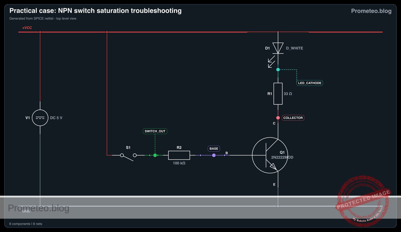
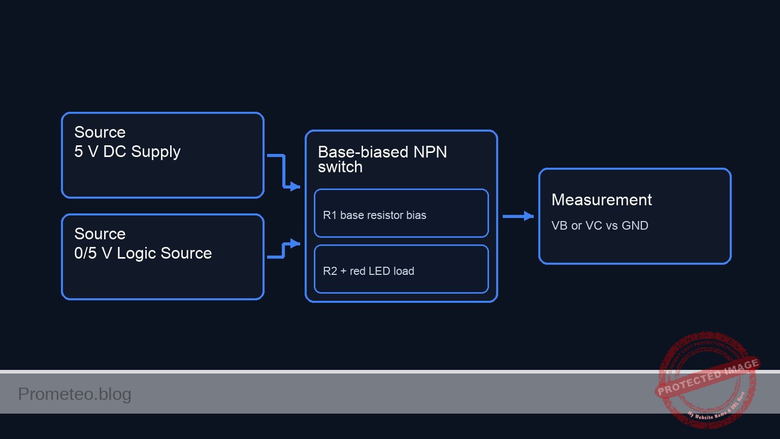
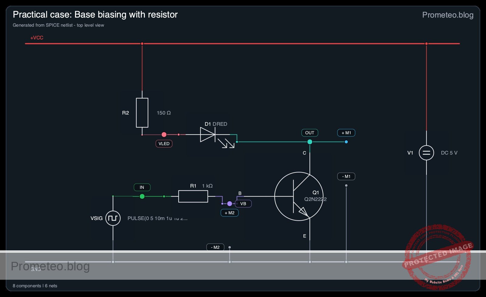
V1: 5 V DC supplyVSIG: 0 V / 5 V logic source, function: control signal for transistor baseR1: 1 kΩ resistor, function: base current limitingR2: 150 Ω resistor, function: load current limiting for LED branchD1: red LED, function: visible collector load indicatorQ1: 2N2222 NPN transistor, function: low-side switchM1: digital multimeter, function: voltage and current measurementsM2: optional second multimeter, function: simultaneous current check
Wiring guide
Use these node names: VCC, 0, VIN, VB, VC.
V1connects betweenVCCand0.VSIGconnects betweenVINand0.R1connects betweenVINandVB.Q1collector connects toVC.Q1base connects toVB.Q1emitter connects to0.R2connects betweenVCCand the anode node ofD1.D1anode connects toR2;D1cathode connects toVC.
Practical design values:
– Load current target: about Ic = (5 V - 2.0 V - 0.2 V) / 150 Ω ≈ 18.7 mA
– Forced gain for saturation: use β_forced ≈ 10
– Required base current: Ib ≈ Ic / 10 ≈ 1.9 mA
– Base resistor estimate: R1 ≈ (5 V - 0.7 V) / 1.9 mA ≈ 2.26 kΩ
To make switching more robust, choose a lower standard value:
– Selected R1 = 1 kΩ
– Expected base current: Ib ≈ (5 V - 0.7 V) / 1 kΩ ≈ 4.3 mA
This value is suitable only if the logic output can safely source at least 4.3 mA.
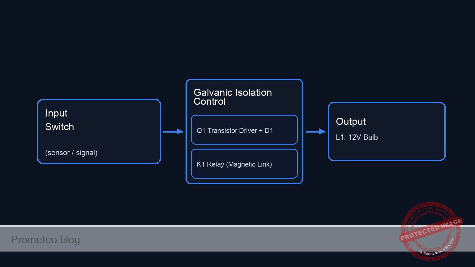
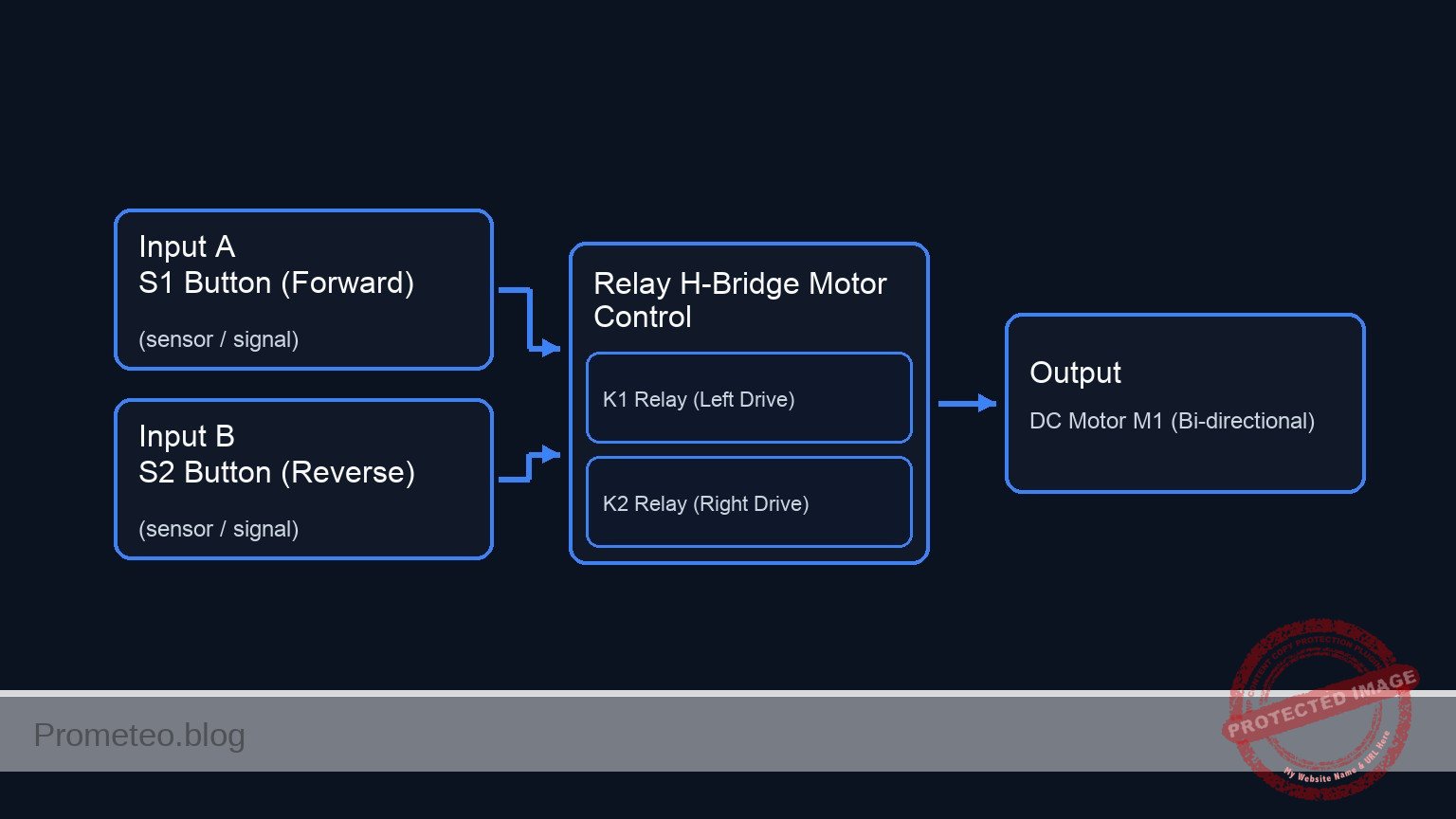
Conceptual block diagram
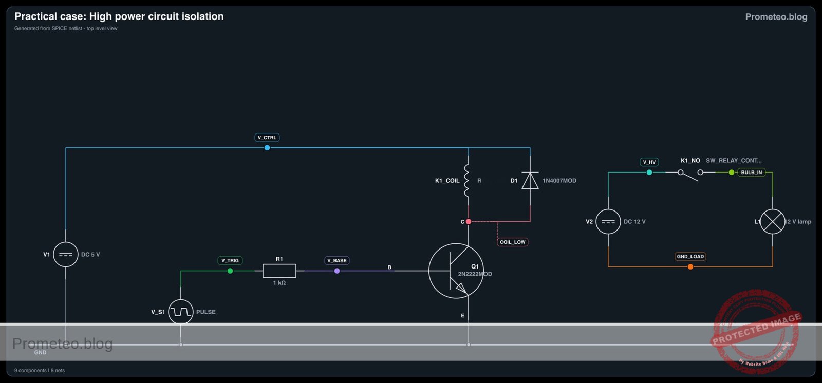
Schematic
Practical case: Base Biasing with Resistor

Power / load path:
[ V1: 5 V DC Supply ] --(VCC)--> [ R2: 150 ohm ] --(LED current limit)--> [ D1: Red LED ] --(cathode at VC)--> [ Q1:C 2N2222 ]
[ Q1:C 2N2222 ] --(collector-emitter path)--> [ Q1:E 2N2222 ] --(0 / GND)--> [ V1: 0 V ]

Control / base path:
[ VSIG: 0/5 V Logic Source ] --(VIN)--> [ R1: 1 kohm ] --(VB)--> [ Q1:B 2N2222 ]
[ Q1:B 2N2222 ] --(base-emitter junction)--> [ Q1:E 2N2222 ] --(0 / GND)--> [ VSIG: 0 V ]

Node labels:
[ VIN ] --> [ R1 ] --> [ VB ] --> [ Q1:B ]
[ VCC ] --> [ R2 ] --> [ D1 Anode ]
[ D1 Cathode ] --> [ VC ] --> [ Q1:C ]
[ Q1:E ] --> [ 0 / GND ]

Optional measurements:
[ M1 DMM ] --(measure V_B or V_C vs 0)--> [ VB / VC ] --> [ 0 / GND ]
[ M2 DMM ] --(current mode, inserted in series where needed)--> [ Base path or Load path ]
Electrical diagram
Measurements and tests
- Power-off check
- Verify all connections before applying power.
- Confirm
Q1emitter goes to0. -
Confirm
R1is in series betweenVINandVB. -
OFF-state test
- Set
VSIG = 0 V. - Measure
VbfromVBto0: expected near0 V. - Measure
VcefromVCto0: expected near5 V. - Observe
D1: it should be OFF. - Measure
Ib: expected approximately0 mA. -
Measure
Ic: expected approximately0 mA. -
ON-state test
- Set
VSIG = 5 V. - Measure
Vb: expected about0.7 V. - Measure
Vbe: expected about0.65 Vto0.8 V. - Measure
Ibby placing the meter in series withR1: expected about4.3 mA. - Measure
Vc: expected low, typically below0.2 Vto0.3 V. - Measure
Vce: expected below0.2 Vif saturation is achieved. - Measure
Icin series with the collector path: expected about18 mAto20 mA. -
Observe
D1: it should be clearly ON. -
Logic output safety check
- Compare the measured
Ibwith the maximum source current allowed by the logic output. -
If the logic output rating is less than the measured base current, increase
R1. -
Verification calculation
- Compute measured gain in switching mode:
Ic / Ib. - Example with measured values:
19 mA / 4.3 mA ≈ 4.4 -
This is consistent with saturated switching, where the transistor is intentionally overdriven.
-
Pass criteria
Ibdoes not exceed the logic output limit.D1turns fully ON at logic HIGH and fully OFF at logic LOW.Vcein ON state is low enough to confirm saturation.
SPICE netlist and simulation
Reference SPICE Netlist (ngspice) — excerptFull SPICE netlist (ngspice)
* Practical case: Base Biasing with Resistor
.width out=256

V1 VCC 0 DC 5
VSIG VIN 0 PULSE(0 5 10m 1u 1u 245m 1s)

R1 VIN VB 1k
R2 VCC VLED 150
D1 VLED VC DRED
Q1 VC VB 0 Q2N2222

* Optional multimeter loading approximations (high impedance voltmeters)
RM1 VC 0 10Meg
RM2 VB 0 10Meg

* Alias nodes for guaranteed logging
VALIASIN IN VIN 0
VALIASOUT OUT VC 0

.model DRED D(IS=1e-18 N=2.0 RS=10 CJO=20p VJ=0.75 M=0.5 TT=50n BV=5 IBV=10u)
* ... (truncated in public view) ...
Copy this content into a .cir file and run with ngspice.
* Practical case: Base Biasing with Resistor
.width out=256

V1 VCC 0 DC 5
VSIG VIN 0 PULSE(0 5 10m 1u 1u 245m 1s)

R1 VIN VB 1k
R2 VCC VLED 150
D1 VLED VC DRED
Q1 VC VB 0 Q2N2222

* Optional multimeter loading approximations (high impedance voltmeters)
RM1 VC 0 10Meg
RM2 VB 0 10Meg

* Alias nodes for guaranteed logging
VALIASIN IN VIN 0
VALIASOUT OUT VC 0

.model DRED D(IS=1e-18 N=2.0 RS=10 CJO=20p VJ=0.75 M=0.5 TT=50n BV=5 IBV=10u)
.model Q2N2222 NPN(IS=1e-14 BF=200 VAF=100 IKF=0.1 ISE=1e-13 NE=1.5 BR=5 NR=1.0 VAR=25 IKR=0.05
+ RC=0.5 RE=0.2 RB=10 CJE=25p VJE=0.75 MJE=0.33 TF=0.4n XTF=2 CJC=8p VJC=0.55 MJC=0.33 TR=50n)

.save V(IN) V(OUT) V(VIN) V(VC) V(VB) V(VLED) I(V1) I(VSIG)

.op
.print op V(IN) V(OUT) V(VIN) V(VC) V(VB) V(VLED) I(V1) I(VSIG)

.tran 0.1m 250m
.print tran V(IN) V(OUT) V(VIN) V(VC) V(VB) V(VLED) I(V1) I(VSIG)

.end
Simulation Results (Transient Analysis)

Show raw data table (2528 rows)
Index   time            v(in)           v(out)          v(vin)          v(vc)           v(vb)           v(vled)         v1#branch       vsig#branch
0	0.000000e+00	0.000000e+00	3.623103e+00	0.000000e+00	3.623103e+00	3.624741e-09	4.999946e+00	-3.62318e-07	3.624741e-12
1	1.000000e-06	0.000000e+00	3.623104e+00	0.000000e+00	3.623104e+00	6.699379e-09	4.999946e+00	-3.62321e-07	6.699379e-12
2	2.000000e-06	0.000000e+00	3.623105e+00	0.000000e+00	3.623105e+00	6.506970e-09	4.999946e+00	-3.62321e-07	6.506970e-12
3	4.000000e-06	0.000000e+00	3.623106e+00	0.000000e+00	3.623106e+00	5.984372e-09	4.999946e+00	-3.62320e-07	5.984372e-12
4	8.000000e-06	0.000000e+00	3.623108e+00	0.000000e+00	3.623108e+00	5.188535e-09	4.999946e+00	-3.62320e-07	5.188535e-12
5	1.600000e-05	0.000000e+00	3.623110e+00	0.000000e+00	3.623110e+00	4.293865e-09	4.999946e+00	-3.62319e-07	4.293865e-12
6	3.200000e-05	0.000000e+00	3.623112e+00	0.000000e+00	3.623112e+00	3.693772e-09	4.999946e+00	-3.62318e-07	3.693772e-12
7	6.400000e-05	0.000000e+00	3.623112e+00	0.000000e+00	3.623112e+00	3.610539e-09	4.999946e+00	-3.62318e-07	3.610539e-12
8	1.280000e-04	0.000000e+00	3.623112e+00	0.000000e+00	3.623112e+00	3.631021e-09	4.999946e+00	-3.62318e-07	3.631021e-12
9	2.280000e-04	0.000000e+00	3.623112e+00	0.000000e+00	3.623112e+00	3.621414e-09	4.999946e+00	-3.62318e-07	3.621414e-12
10	3.280000e-04	0.000000e+00	3.623112e+00	0.000000e+00	3.623112e+00	3.626121e-09	4.999946e+00	-3.62318e-07	3.626121e-12
11	4.280000e-04	0.000000e+00	3.623112e+00	0.000000e+00	3.623112e+00	3.624676e-09	4.999946e+00	-3.62318e-07	3.624676e-12
12	5.280000e-04	0.000000e+00	3.623112e+00	0.000000e+00	3.623112e+00	3.623957e-09	4.999946e+00	-3.62318e-07	3.623957e-12
13	6.280000e-04	0.000000e+00	3.623112e+00	0.000000e+00	3.623112e+00	3.626113e-09	4.999946e+00	-3.62318e-07	3.626113e-12
14	7.280000e-04	0.000000e+00	3.623112e+00	0.000000e+00	3.623112e+00	3.623011e-09	4.999946e+00	-3.62318e-07	3.623011e-12
15	8.280000e-04	0.000000e+00	3.623112e+00	0.000000e+00	3.623112e+00	3.626745e-09	4.999946e+00	-3.62318e-07	3.626745e-12
16	9.280000e-04	0.000000e+00	3.623112e+00	0.000000e+00	3.623112e+00	3.622584e-09	4.999946e+00	-3.62318e-07	3.622584e-12
17	1.028000e-03	0.000000e+00	3.623112e+00	0.000000e+00	3.623112e+00	3.627045e-09	4.999946e+00	-3.62318e-07	3.627045e-12
18	1.128000e-03	0.000000e+00	3.623112e+00	0.000000e+00	3.623112e+00	3.622367e-09	4.999946e+00	-3.62318e-07	3.622367e-12
19	1.228000e-03	0.000000e+00	3.623112e+00	0.000000e+00	3.623112e+00	3.627168e-09	4.999946e+00	-3.62318e-07	3.627168e-12
20	1.328000e-03	0.000000e+00	3.623112e+00	0.000000e+00	3.623112e+00	3.622305e-09	4.999946e+00	-3.62318e-07	3.622305e-12
21	1.428000e-03	0.000000e+00	3.623112e+00	0.000000e+00	3.623112e+00	3.627229e-09	4.999946e+00	-3.62318e-07	3.627229e-12
22	1.528000e-03	0.000000e+00	3.623112e+00	0.000000e+00	3.623112e+00	3.622257e-09	4.999946e+00	-3.62318e-07	3.622257e-12
23	1.628000e-03	0.000000e+00	3.623112e+00	0.000000e+00	3.623112e+00	3.627228e-09	4.999946e+00	-3.62318e-07	3.627228e-12
... (2504 more rows) ...
Common mistakes and how to avoid them
- Using no base resistor
- Error: connecting the logic output directly to the transistor base.
- Result: excessive base current and possible damage to the logic output.
-
Fix: always place
R1betweenVINandVB. -
Choosing a base resistor that is too large
- Error: using
R1 = 10 kΩwithout checking current. - Result: base current may be too low, so the transistor may not saturate.
-
Fix: calculate
Ibfrom the load current and use a forced gain of about 10 for switching. -
Reversing transistor terminals
- Error: swapping collector and emitter.
- Result: abnormal voltages, weak load current, or no switching.
- Fix: confirm the 2N2222 pinout from its datasheet before wiring.
Troubleshooting
- Symptom: LED never turns ON
- Cause:
VSIGis not reaching 5 V, orQ1base is not connected throughR1. -
Fix: measure
VINandVB; verifyR1continuity and transistor pinout. -
Symptom: LED is dim
- Cause: transistor is not saturated because
R1is too large. -
Fix: reduce
R1after checking the logic output current limit. -
Symptom: Logic output voltage drops when ON
- Cause: base current demand is too high for the logic source.
-
Fix: increase
R1or use a transistor driver stage. -
Symptom: LED stays ON all the time
- Cause: wrong wiring at the collector node or unintended base bias.
-
Fix: check that
Q1emitter is at0and thatVINactually goes to 0 V in the LOW state. -
Symptom: Measured
Vceis high when ON - Cause: insufficient base current or incorrect collector load wiring.
- Fix: verify
Ib, recalculateR1, and checkR2andD1orientation.
Possible improvements and extensions
- Add a
10 kΩpull-down resistor fromVBto0so the transistor stays OFF if the logic source becomes disconnected or high-impedance. - Replace the LED load with a relay coil and add a flyback diode across the coil to study transistor switching with inductive loads.
More Practical Cases on Prometeo.blog
Find this product and/or books on this topic on Amazon
As an Amazon Associate, I earn from qualifying purchases. If you buy through this link, you help keep this project running.
Quick Quiz

Telecommunications Electronics Engineer and Computer Engineer (official degrees in Spain).