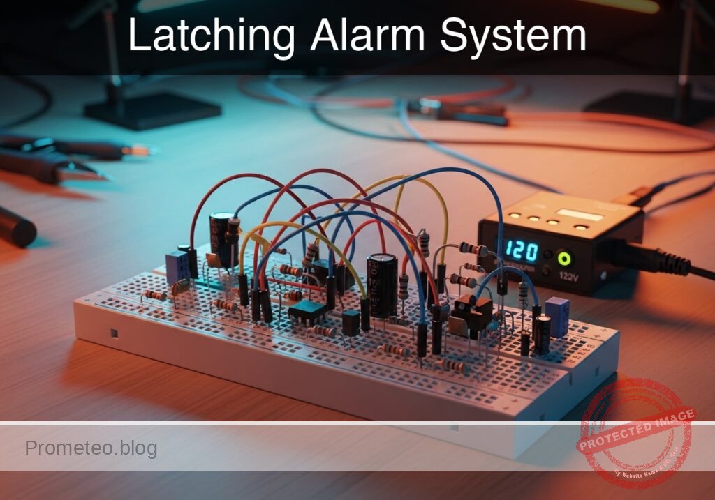
Level: Basic. Build a self-latching relay circuit to maintain an alarm state after a momentary trigger.
Objective and use case
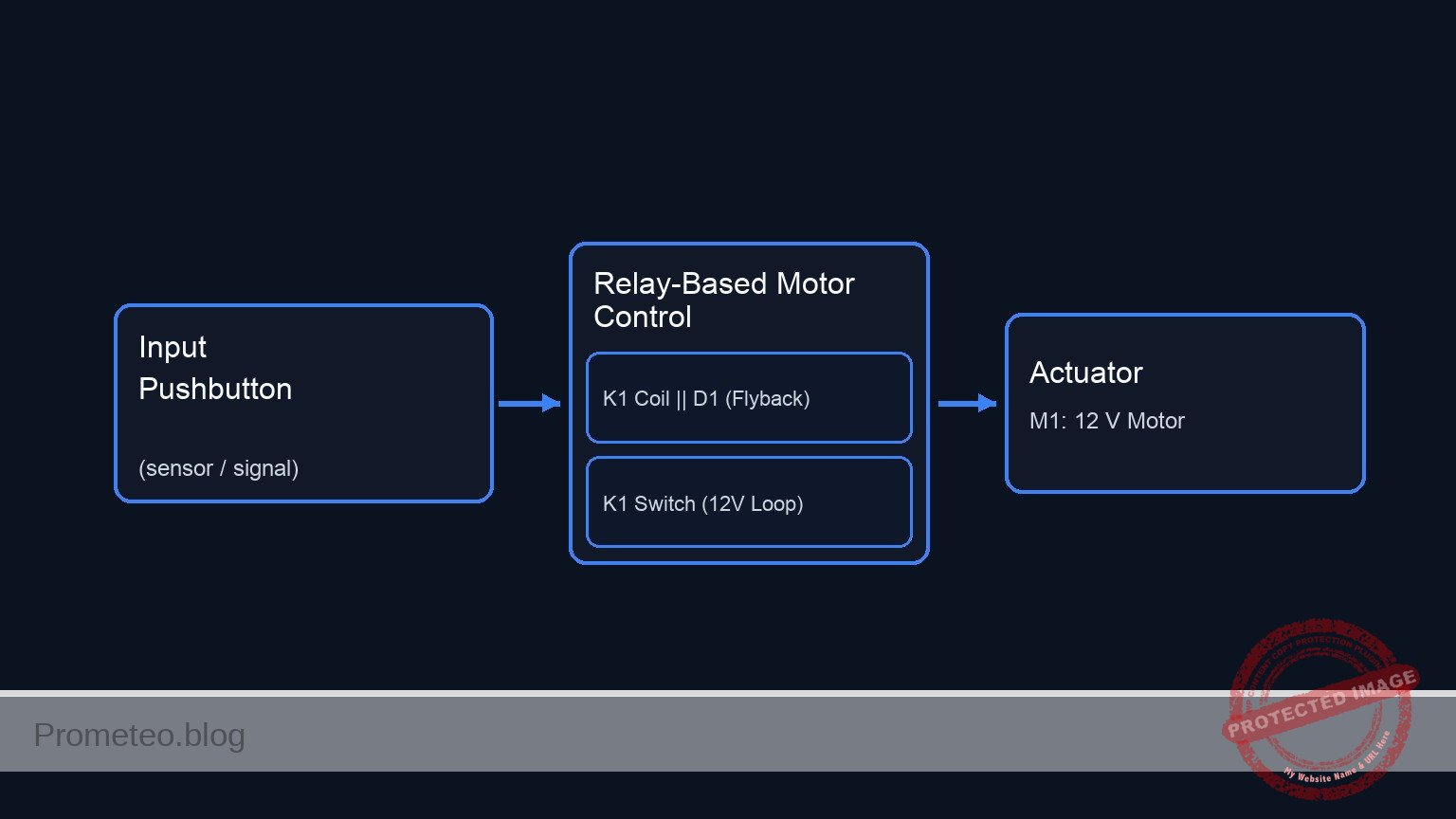
You will build a basic «memory» circuit using an electromechanical relay, often called a latching or holding circuit. A momentary press of a trigger button will activate an alarm (LED), which will remain active even after the button is released, until a separate reset button is pressed.
- Security Systems: Used in simple burglar alarms where a tripped sensor keeps the siren on until a user resets it.
- Industrial Safety: Commonly used in «Start/Stop» motor control stations.
- Fault Indicators: Captures transient error signals so operators can see a fault occurred even if the condition clears.
Expected outcome:
* Initial state: LED is OFF.
* Action 1: Momentarily press the «Trigger» button → LED turns ON and relay clicks.
* Action 2: Release «Trigger» button → LED remains ON (Latched).
* Action 3: Press «Reset» button → LED turns OFF and relay releases.
Target audience: Beginners familiar with basic circuits and relay operation.
Materials
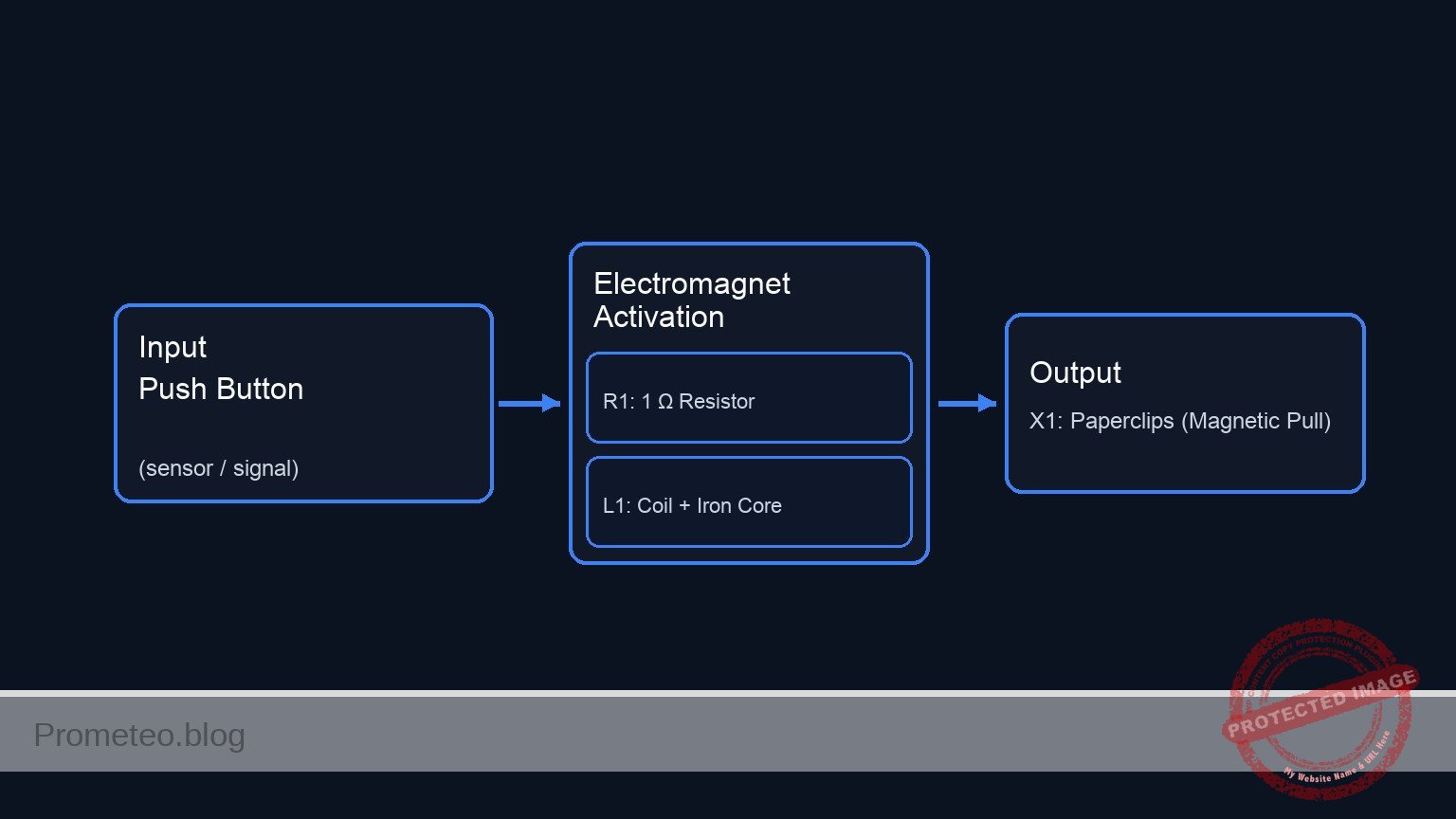
- V1: 12 V DC power supply, function: Main power source
- K1: SPDT Relay (12 V Coil), function: Electromechanical switch and memory element
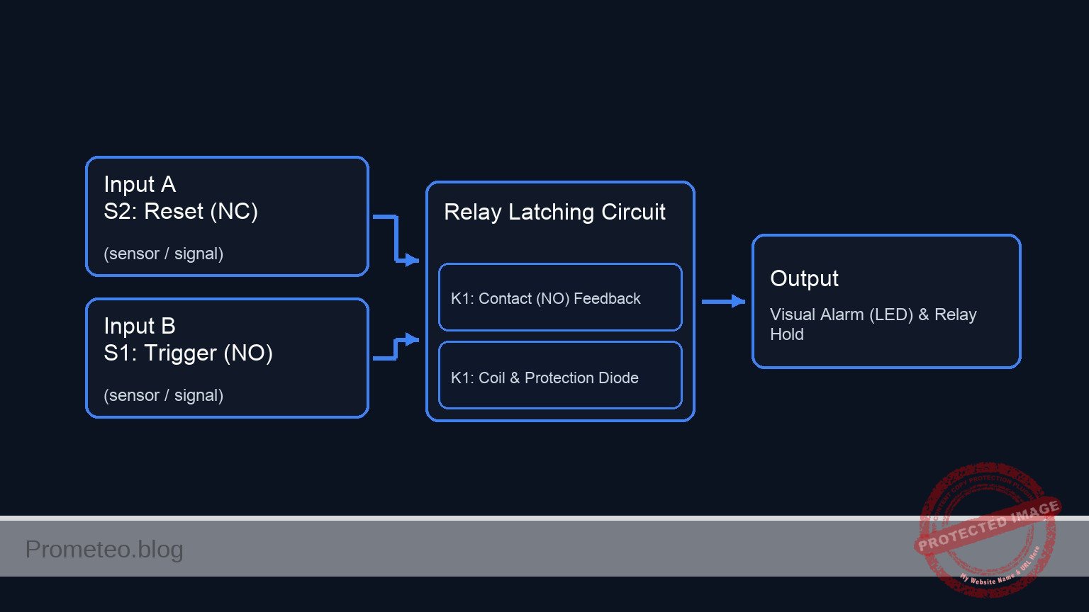
- S1: Pushbutton (Normally Open – NO), function: Trigger signal
- S2: Pushbutton (Normally Closed – NC), function: Reset signal
- R1: 1 kΩ resistor, function: Current limiting for LED
- D1: Red LED, function: Visual alarm indicator
- D2: 1N4007 Diode, function: Flyback protection for the coil
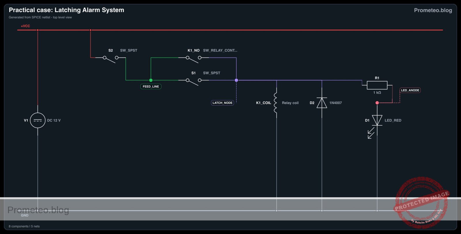
Wiring guide
Connect the components using the following node definitions: VCC (12 V), 0 (Ground), feed_line, latch_node.
- V1 (DC Source): Connect Positive to
VCCand Negative to0. - S2 (Reset Button – NC): Connect between
VCCandfeed_line. - S1 (Trigger Button – NO): Connect between
feed_lineandlatch_node. - K1 (Relay Coil): Connect one side to
latch_nodeand the other side to0. - K1 (Relay Common Contact – COM): Connect to
feed_line. - K1 (Relay Normally Open Contact – NO): Connect to
latch_node. - D2 (Protection Diode): Connect Cathode (stripe) to
latch_nodeand Anode to0. - R1 (Resistor): Connect between
latch_nodeand nodeled_anode. - D1 (LED): Connect Anode to
led_anodeand Cathode to0.
Note: S2 allows current to flow to the circuit. S1 initially energizes the coil. Once K1 energizes, the COM-NO internal connection bypasses S1, keeping the coil powered from the feed_line.
Conceptual block diagram
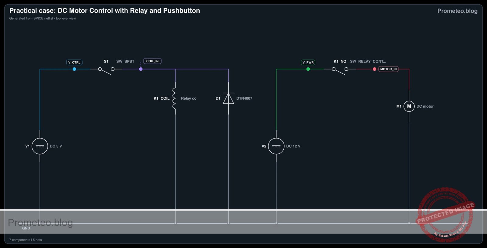
Schematic
Title: Practical case: Latching Alarm System

      (Main Power)
        VCC 12 V
           |
           V
  [ S2: Reset (NC) ]
           |
      (feed_line)
           |
           |    (Path A: Manual Trigger)
           +--> [ S1: Trigger (NO) ] ------------------+
           |                                           |
           |                                           V
           |                                     (latch_node)
           |                                           |
           |    (Path B: Self-Latching)                +----------> [ R1: 1k ] --> [ D1: LED ] --> GND
           +--> [ K1: Contact (NO) ] ------------------+           (Visual Alarm)
                         ^                             |
                         |                             |
                         |                             +----------> [ K1: Coil || D2(Rev) ] --> GND
                         |                                         (Relay Magnet & Protection)
                         |                                                  |
                         +----------------(Magnetic Link)-------------------+
Electrical diagram
Measurements and tests
Follow these steps to validate the latching behavior:
- Coil Continuity Check: Before applying power, use a multimeter in Ohms mode to measure the relay coil pins. You should read a resistance value (typically 100 Ω to 400 Ω depending on the relay).
- Standby Check: Power on the circuit. Measure voltage between
latch_nodeand0. It should be 0 V. The LED should be OFF. - Trigger Test: Press and hold S1. Measure voltage at
latch_node. It should rise to approx 12 V. The LED should turn ON. - Latching Test: Release S1. The voltage at
latch_nodemust remain at 12 V, and the LED must stay ON. Listen for the relay; it should not click off. - Reset Test: Press S2 (Reset). The voltage at
latch_nodeshould drop to 0 V instantly. The LED turns OFF. Release S2; the LED remains OFF.
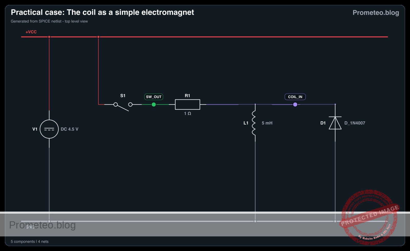
SPICE netlist and simulation
Reference SPICE Netlist (ngspice) — excerptFull SPICE netlist (ngspice)
* Latching Alarm System
.width out=256
* Based on Practical Breadboard Case

* ==========================================
* Power Supply
* ==========================================
* V1: 12V Main Supply
V1 VCC 0 DC 12

* ==========================================
* Control Inputs (User Stimuli)
* ==========================================
* S1 (Trigger Button - NO):
* Simulating a press (Close) at 10ms for 5ms duration.
* Pulse: 0V (Open) -> 5V (Closed) -> 0V (Open)
V_S1_ctrl ctrl_s1 0 PULSE(0 5 10m 100u 100u 5m 100m)

* S2 (Reset Button - NC):
* Simulating a press (Open) at 40ms for 5ms duration.
* ... (truncated in public view) ...
Copy this content into a .cir file and run with ngspice.
* Latching Alarm System
.width out=256
* Based on Practical Breadboard Case

* ==========================================
* Power Supply
* ==========================================
* V1: 12V Main Supply
V1 VCC 0 DC 12

* ==========================================
* Control Inputs (User Stimuli)
* ==========================================
* S1 (Trigger Button - NO):
* Simulating a press (Close) at 10ms for 5ms duration.
* Pulse: 0V (Open) -> 5V (Closed) -> 0V (Open)
V_S1_ctrl ctrl_s1 0 PULSE(0 5 10m 100u 100u 5m 100m)

* S2 (Reset Button - NC):
* Simulating a press (Open) at 40ms for 5ms duration.
* Pulse: 5V (Closed/Idle) -> 0V (Open/Pressed) -> 5V (Closed/Idle)
* Note: This voltage represents the connectivity state (High = Conducting).
V_S2_ctrl ctrl_s2 0 PULSE(5 0 40m 100u 100u 5m 100m)

* ==========================================
* Circuit Components
* ==========================================

* S2: Reset Switch (NC)
* Connects VCC to feed_line.
* Controlled by ctrl_s2 (Active High logic for NC behavior).
S2 VCC feed_line ctrl_s2 0 SW_IDEAL

* S1: Trigger Switch (NO)
* Connects feed_line to latch_node.
* Controlled by ctrl_s1 (Active High logic for NO behavior).
S1 feed_line latch_node ctrl_s1 0 SW_IDEAL

* K1: Relay Implementation
* 1. Coil: Modeled as Inductance + Series Resistance
*    Connects latch_node to Ground (0).
*    100 Ohm resistance is typical for a 12V relay coil.
R_coil latch_node k1_internal 100
L_coil k1_internal 0 10m

* 2. Relay Contact (Switch):
*    Connects feed_line (COM) to latch_node (NO).
*    Controlled by the voltage across the coil (latch_node).
*    Threshold set to 6V (Pull-in) with hysteresis.
S_relay feed_line latch_node latch_node 0 SW_RELAY

* D2: Flyback Protection Diode
* Cathode to latch_node, Anode to 0.
D2 0 latch_node 1N4007

* Alarm Indicator (LED + Resistor)
* R1: Current limiting
R1 latch_node led_anode 1k
* D1: Red LED
D1 led_anode 0 LED_RED

* Floating Node Prevention
* High impedance pull-down for feed_line when S2 opens
R_float feed_line 0 100Meg

* ==========================================
* Models
* ==========================================
* Ideal switch for buttons (Vt=2.5V logic threshold)
.model SW_IDEAL SW(Vt=2.5 Ron=0.01 Roff=100Meg)

* Relay switch model (Picks up at 6V, drops out at 4V)
.model SW_RELAY SW(Vt=6 Vh=2 Ron=0.01 Roff=100Meg)

* 1N4007 Diode Model
.model 1N4007 D(Is=7n Rs=0.04 N=1.5 Cjo=20p BV=1000 IBV=5u)

* Generic Red LED Model
.model LED_RED D(Is=1a N=4 Rs=4)

* ==========================================
* Simulation Directives
* ==========================================
* Transient analysis: 100us step, 60ms total time
* Covers Trigger (10ms) and Reset (40ms) events
.tran 100u 60m

* Output variables
* V(latch_node) is the ALARM STATE (Output)
* V(feed_line) shows power delivery
.print tran V(latch_node) V(feed_line) V(ctrl_s1) V(ctrl_s2) I(L_COIL)

.op
.end
Simulation Results (Transient Analysis)

Show raw data table (2796 rows)
Index   time            v(latch_node)   v(feed_line)    v(ctrl_s1)      v(ctrl_s2)      l_coil#branch
0	0.000000e+00	2.399952e-05	1.200000e+01	0.000000e+00	5.000000e+00	2.399952e-07
1	1.000000e-06	2.399953e-05	1.200000e+01	0.000000e+00	5.000000e+00	2.399952e-07
2	2.000000e-06	2.399952e-05	1.200000e+01	0.000000e+00	5.000000e+00	2.399952e-07
3	4.000000e-06	2.399952e-05	1.200000e+01	0.000000e+00	5.000000e+00	2.399952e-07
4	8.000000e-06	2.399952e-05	1.200000e+01	0.000000e+00	5.000000e+00	2.399952e-07
5	1.600000e-05	2.399952e-05	1.200000e+01	0.000000e+00	5.000000e+00	2.399952e-07
6	3.200000e-05	2.399952e-05	1.200000e+01	0.000000e+00	5.000000e+00	2.399952e-07
7	6.400000e-05	2.399952e-05	1.200000e+01	0.000000e+00	5.000000e+00	2.399952e-07
8	1.280000e-04	2.399952e-05	1.200000e+01	0.000000e+00	5.000000e+00	2.399952e-07
9	2.280000e-04	2.399952e-05	1.200000e+01	0.000000e+00	5.000000e+00	2.399952e-07
10	3.280000e-04	2.399952e-05	1.200000e+01	0.000000e+00	5.000000e+00	2.399952e-07
11	4.280000e-04	2.399952e-05	1.200000e+01	0.000000e+00	5.000000e+00	2.399952e-07
12	5.280000e-04	2.399952e-05	1.200000e+01	0.000000e+00	5.000000e+00	2.399952e-07
13	6.280000e-04	2.399952e-05	1.200000e+01	0.000000e+00	5.000000e+00	2.399952e-07
14	7.280000e-04	2.399952e-05	1.200000e+01	0.000000e+00	5.000000e+00	2.399952e-07
15	8.280000e-04	2.399952e-05	1.200000e+01	0.000000e+00	5.000000e+00	2.399952e-07
16	9.280000e-04	2.399952e-05	1.200000e+01	0.000000e+00	5.000000e+00	2.399952e-07
17	1.028000e-03	2.399952e-05	1.200000e+01	0.000000e+00	5.000000e+00	2.399952e-07
18	1.128000e-03	2.399952e-05	1.200000e+01	0.000000e+00	5.000000e+00	2.399952e-07
19	1.228000e-03	2.399952e-05	1.200000e+01	0.000000e+00	5.000000e+00	2.399952e-07
20	1.328000e-03	2.399952e-05	1.200000e+01	0.000000e+00	5.000000e+00	2.399952e-07
21	1.428000e-03	2.399952e-05	1.200000e+01	0.000000e+00	5.000000e+00	2.399952e-07
22	1.528000e-03	2.399952e-05	1.200000e+01	0.000000e+00	5.000000e+00	2.399952e-07
23	1.628000e-03	2.399952e-05	1.200000e+01	0.000000e+00	5.000000e+00	2.399952e-07
... (2772 more rows) ...
Common mistakes and how to avoid them
- Using a Normally Open button for Reset: If S2 is NO instead of NC, the circuit will never receive power to start. Ensure S2 conducts current by default.
- Connecting the latch to NC contact: If you connect the
latch_nodeto the Relay’s NC pin instead of NO, the relay will turn on immediately upon power-up and oscillate or buzz (buzzer effect). Always use the NO pin for self-latching. - LED burns out immediately: Forgetting R1 allows excessive current through the LED. Always verify the resistor value before powering up.
Troubleshooting
- Symptom: LED turns on when S1 is pressed but turns off immediately when released.
- Cause: The latching path is broken.
- Fix: Check the connection between K1 (COM), K1 (NO), and the
latch_node. Ensure the relay contacts are parallel to S1.
- Symptom: Relay buzzes loudly or chatters.
- Cause: Power supply voltage is too low or unstable.
- Fix: Ensure V1 provides stable 12 V and can supply enough current for the coil.
- Symptom: Circuit cannot be reset.
- Cause: S2 is bypassed or faulty (shorted).
- Fix: Check S2 with a multimeter; it must break the connection (Open) when pressed.
Possible improvements and extensions
- Audible Alarm: Connect a 12 V active buzzer in parallel with the LED (between
latch_nodeand0) to add sound to the alarm. - High Power Control: Use a DPDT relay. Use the first set of contacts for the 12 V logic latching (as described above) and the second set of contacts to switch a completely separate high-voltage load, like a 120 V/230 V lamp.
More Practical Cases on Prometeo.blog
Find this product and/or books on this topic on Amazon
As an Amazon Associate, I earn from qualifying purchases. If you buy through this link, you help keep this project running.
Quick Quiz

Telecommunications Electronics Engineer and Computer Engineer (official degrees in Spain).