Nivel: Medio — Diseñar y analizar un circuito que atenúa las frecuencias altas utilizando un condensador y una resistencia para verificar la frecuencia de corte.
Objetivo y caso de uso
En este caso práctico, construirá un Filtro Paso Bajo (LPF) pasivo de primer orden utilizando una resistencia y un condensador conectados en serie. Analizará cómo cambia la reactancia del condensador con la frecuencia, permitiendo el paso de frecuencias bajas mientras atenúa las señales por encima de un punto de corte calculado.
Por qué es útil:
* Reducción de ruido de audio: Elimina el siseo de alta frecuencia o la estática de las grabaciones de audio.
* Crossovers para subwoofers: Dirige solo las notas graves de baja frecuencia al controlador (driver) del subwoofer.
* Acondicionamiento de señal: Actúa como filtro anti-aliasing antes de la Conversión Analógico-Digital (ADC) para prevenir artefactos digitales.
* Suavizado de fuente de alimentación: Filtra el ruido de rizado de alta frecuencia de las líneas de alimentación de CC.
Resultado esperado:
* Banda de paso: Las frecuencias por debajo de ~1 kHz conservan aproximadamente su amplitud original (Vin ≈ Vout).
* Punto de corte: En la frecuencia de corte calculada (fc), el voltaje de salida cae a aproximadamente el 70,7% del voltaje de entrada (-3 dB).
* Banda de rechazo: Las frecuencias significativamente superiores a 1 kHz son fuertemente atenuadas.
* Desfase: Observar un retraso de fase de -45° en la frecuencia de corte.
Público objetivo y nivel: Estudiantes de electrónica y entusiastas del audio; Nivel: Medio.
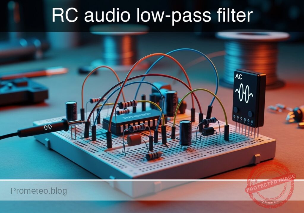
Materiales
- V1: Fuente de voltaje CA (Onda senoidal, 5 Vpk, frecuencia ajustable), función: Simulación de señal de audio de entrada.
- R1: Resistencia de 1.6 kΩ, función: Limitación de corriente y parte del divisor de voltaje.
- C1: Condensador de 100 nF (cerámico o de película), función: Derivación a tierra dependiente de la frecuencia.
- Herramienta de medición: Osciloscopio (doble canal) o Trazador de Bode.
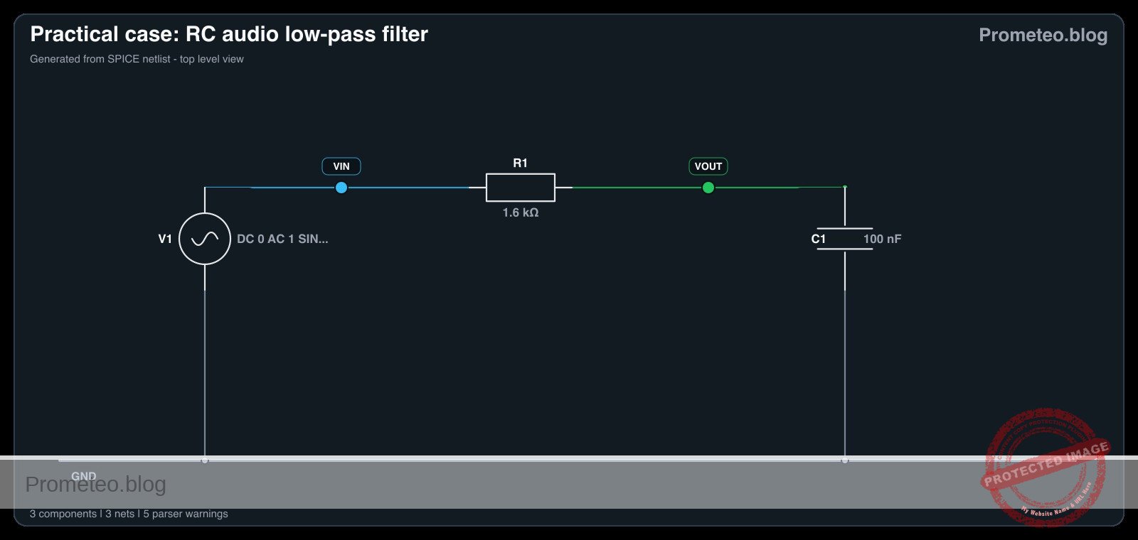
Guía de conexionado
Construya el circuito utilizando las siguientes conexiones. Observe los nombres de nodo explícitos para el análisis.
- V1 (Fuente): Conecte el terminal positivo al nodo
VINy el terminal negativo al nodo0(GND). - R1: Conecte una patilla al nodo
VINy la otra patilla al nodoVOUT. - C1: Conecte una patilla al nodo
VOUTy la otra patilla al nodo0(GND). - Osciloscopio Ch1: Conecte la punta de la sonda a
VINy la pinza de tierra a0. - Osciloscopio Ch2: Conecte la punta de la sonda a
VOUTy la pinza de tierra a0.
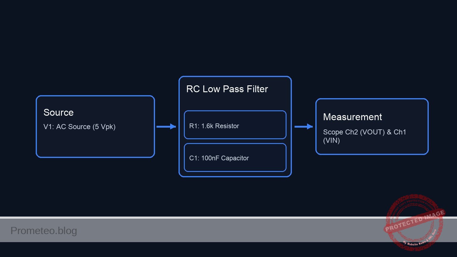
Diagrama de bloques conceptual
Esquemático
[ SIGNAL SOURCE ]               [ RC FILTER STAGE ]                 [ MEASUREMENT ]

                                       +--------------------------------------> [ Scope Ch1 (Input) ]
                              |
[ V1: AC Source ] --(VIN)-->--+--> [ R1: 1.6k Resistor ] --(VOUT)-->--+--> [ Scope Ch2 (Output) ]
      (5 Vpk)                                                         |
                                                                      +--> [ C1: 100nF Cap ] --> GND
Diagrama eléctrico

Mediciones y pruebas
Siga estos pasos para validar el diseño del filtro (fc ≈ 1 kHz):
-
Prueba de baja frecuencia (Banda de paso):
- Ajuste V1 a 100 Hz.
- Mida el valor pico a pico de Vout. Debería ser casi idéntico a Vin (aprox. 5 V).
-
Verificación de frecuencia de corte (fc):
- Aumente la frecuencia de V1 a 1 kHz.
- Mida Vout. Debería caer a aproximadamente 0.707 × Vin (aprox. 3.53 V).
- Mida la diferencia de fase entre Ch1 y Ch2. Vout debería retrasarse respecto a Vin aproximadamente 45°.
-
Prueba de alta frecuencia (Banda de rechazo):
- Ajuste V1 a 10 kHz (una década por encima del corte).
- Mida Vout. La amplitud debería estar significativamente atenuada (aprox. 0.5 V o -20 dB en relación con la entrada).
-
Análisis de diagrama de Bode (Opcional):
- Si utiliza una simulación o un trazador de Bode, realice un barrido de 10 Hz a 100 kHz. Observe la pendiente de «caída» de -20 dB/década después del punto de corte.
Netlist SPICE y simulación
Netlist SPICE de referencia (ngspice) — extractoNetlist SPICE completo (ngspice)
* Practical case: RC audio low-pass filter

* --- Components per BOM and Wiring Guide ---
* V1: AC Voltage Source (Sine Wave, 5 Vpk, 1kHz, AC 1V for Bode)
* Connected: Positive -> VIN, Negative -> 0 (GND)
V1 VIN 0 DC 0 AC 1 SIN(0 5 1000)

* R1: 1.6 kOhm resistor
* Connected: VIN -> VOUT
R1 VIN VOUT 1.6k

* C1: 100 nF capacitor
* Connected: VOUT -> 0 (GND)
C1 VOUT 0 100n

* --- Simulation Commands ---
* Using .control block to sequence analyses and printing correctly in ngspice
.control
    * Transient Analysis: 1kHz signal, run for 5ms
    tran 10u 5ms
* ... (truncated in public view) ...
Copia este contenido en un archivo .cir y ejecútalo con ngspice.
* Practical case: RC audio low-pass filter

* --- Components per BOM and Wiring Guide ---
* V1: AC Voltage Source (Sine Wave, 5 Vpk, 1kHz, AC 1V for Bode)
* Connected: Positive -> VIN, Negative -> 0 (GND)
V1 VIN 0 DC 0 AC 1 SIN(0 5 1000)

* R1: 1.6 kOhm resistor
* Connected: VIN -> VOUT
R1 VIN VOUT 1.6k

* C1: 100 nF capacitor
* Connected: VOUT -> 0 (GND)
C1 VOUT 0 100n

* --- Simulation Commands ---
* Using .control block to sequence analyses and printing correctly in ngspice
.control
    * Transient Analysis: 1kHz signal, run for 5ms
    tran 10u 5ms
    * Print transient results (Oscilloscope)
    print V(VIN) V(VOUT)

    * AC Analysis: Bode Plot, 10 Hz to 100 kHz
    ac dec 10 10 100k
    * Print AC results (Bode Plotter)
    print V(VOUT)

    * Operating Point
    op
.endc

.end
Resultados de Simulación (Transitorio)

Show raw data table (512 rows)
Index   time            v(vin)          v(vout)
0	0.000000e+00	0.000000e+00	0.000000e+00
1	1.000000e-07	3.141592e-03	1.962269e-06
2	1.084035e-07	3.405596e-03	2.141025e-06
3	1.252105e-07	3.933604e-03	2.526248e-06
4	1.588245e-07	4.989618e-03	3.462948e-06
5	2.260525e-07	7.101647e-03	6.001184e-06
6	3.605086e-07	1.132570e-02	1.373560e-05
7	6.294206e-07	1.977378e-02	3.982505e-05
8	1.167245e-06	3.666975e-02	1.343969e-04
9	2.242893e-06	7.046023e-02	4.923968e-04
10	4.394190e-06	1.380300e-01	1.878099e-03
11	8.696783e-06	2.730815e-01	7.282571e-03
12	1.730197e-05	5.424874e-01	2.825846e-02
13	2.730197e-05	8.535162e-01	6.884897e-02
14	3.730197e-05	1.161176e+00	1.257276e-01
15	4.730197e-05	1.464254e+00	1.976662e-01
16	5.730197e-05	1.761553e+00	2.834382e-01
17	6.730197e-05	2.051900e+00	3.818193e-01
18	7.730197e-05	2.334149e+00	4.915893e-01
19	8.730197e-05	2.607186e+00	6.115335e-01
20	9.730197e-05	2.869934e+00	7.404442e-01
21	1.073020e-04	3.121356e+00	8.771230e-01
22	1.173020e-04	3.360458e+00	1.020383e+00
23	1.273020e-04	3.586299e+00	1.169049e+00
... (488 more rows) ...
Errores comunes y cómo evitarlos
- Intercambiar componentes (Paso alto vs. Paso bajo):
- Error: Conectar C1 en serie y R1 a tierra crea un filtro Paso Alto.
- Solución: Asegúrese de que el Condensador sea el componente conectado entre el nodo de salida y Tierra.
- Ignorar la impedancia de carga:
- Error: Conectar una carga de baja impedancia (como un altavoz de 8 Ω) directamente a
VOUT. - Solución: Este filtro pasivo tiene una alta impedancia de salida. Utilice un búfer con amplificador operacional si maneja una carga pesada.
- Error: Conectar una carga de baja impedancia (como un altavoz de 8 Ω) directamente a
- Usar condensadores polarizados incorrectamente:
- Error: Usar un condensador electrolítico con polaridad inversa en un circuito de CA sin una polarización de CC.
- Solución: Para señales de audio de CA pura, utilice condensadores no polarizados (cerámicos, de película o electrolíticos bipolares).
Solución de problemas
- Síntoma: Vout es cero en todas las frecuencias.
- Causa: Cortocircuito en C1 o circuito abierto en R1.
- Solución: Verifique la continuidad en C1; si pita, el condensador está en corto o el nodo está conectado a tierra accidentalmente.
- Síntoma: No se produce atenuación en frecuencias altas.
- Causa: C1 está abierto (roto) o R1 está en corto.
- Solución: Reemplace C1. Verifique que R1 mida 1.6 kΩ.
- Síntoma: La frecuencia de corte es totalmente incorrecta.
- Causa: Valores de componentes incorrectos (por ejemplo, usar 100 pF en lugar de 100 nF).
- Solución: Verifique los códigos de colores en las resistencias y las marcas en los condensadores (código 104 = 100 nF).
Posibles mejoras y extensiones
- Filtro de segundo orden: Conecte en cascada dos etapas RC en serie para lograr una caída más pronunciada (-40 dB/década) para un mejor rechazo del ruido.
- Filtro paso bajo activo: Añada un Amplificador Operacional (Op-Amp) para crear un filtro activo, permitiendo ganancia de señal y evitando que la carga afecte la respuesta de frecuencia del filtro.
Más Casos Prácticos en Prometeo.blog
Encuentra este producto y/o libros sobre este tema en Amazon
Como afiliado de Amazon, gano con las compras que cumplan los requisitos. Si compras a través de este enlace, ayudas a mantener este proyecto.
Quiz rápido

Ingeniero Superior en Electrónica de Telecomunicaciones e Ingeniero en Informática (titulaciones oficiales en España).