Caso práctico: Medición de corriente con shunt

Prototipo de Medición de corriente con shunt (Maker Style)

Nivel: Medio – Utilice una resistencia de muy bajo valor para medir indirectamente la corriente de una carga de CC a través de la caída de tensión.

Objetivo y caso de uso

Construirá un circuito de corriente continua (CC) que cuenta con una carga ficticia (dummy load) principal y una resistencia en serie de bajo valor, conocida como shunt. Al medir la pequeña caída de tensión a través de este shunt, calculará indirectamente la corriente total que fluye por el circuito utilizando la Ley de Ohm.

Por qué es útil:
* Medición segura de alta corriente: Evita hacer pasar corrientes masivas directamente a través de los circuitos internos, potencialmente frágiles, de su multímetro.
* Monitorización continua: Permite que los microcontroladores o paneles analógicos realicen un seguimiento constante del consumo de energía sin abrir el circuito.
* Protección contra sobrecorriente: Proporciona una señal de tensión proporcional que puede activar un mecanismo de apagado si la corriente excede los límites seguros.
* Reducción de la tensión de carga (burden voltage): Personalizar el tamaño del shunt minimiza la interferencia que el instrumento de medición impone sobre el circuito en funcionamiento.

Resultado esperado:
* Generará una caída de tensión medible en el rango de los milivoltios a través de la resistencia shunt de lado bajo (low-side).
* Calculará correctamente la corriente de la carga ($I = V/R$) a partir de la tensión observada.
* Verificará la disipación de potencia (P = I^2 × R) del shunt para asegurar que opera dentro de límites térmicos seguros.

Público objetivo y nivel: Estudiantes de electrónica de nivel intermedio que aprenden técnicas de medición indirecta y cálculos de potencia.

Materiales

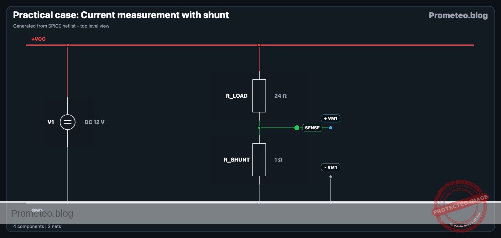
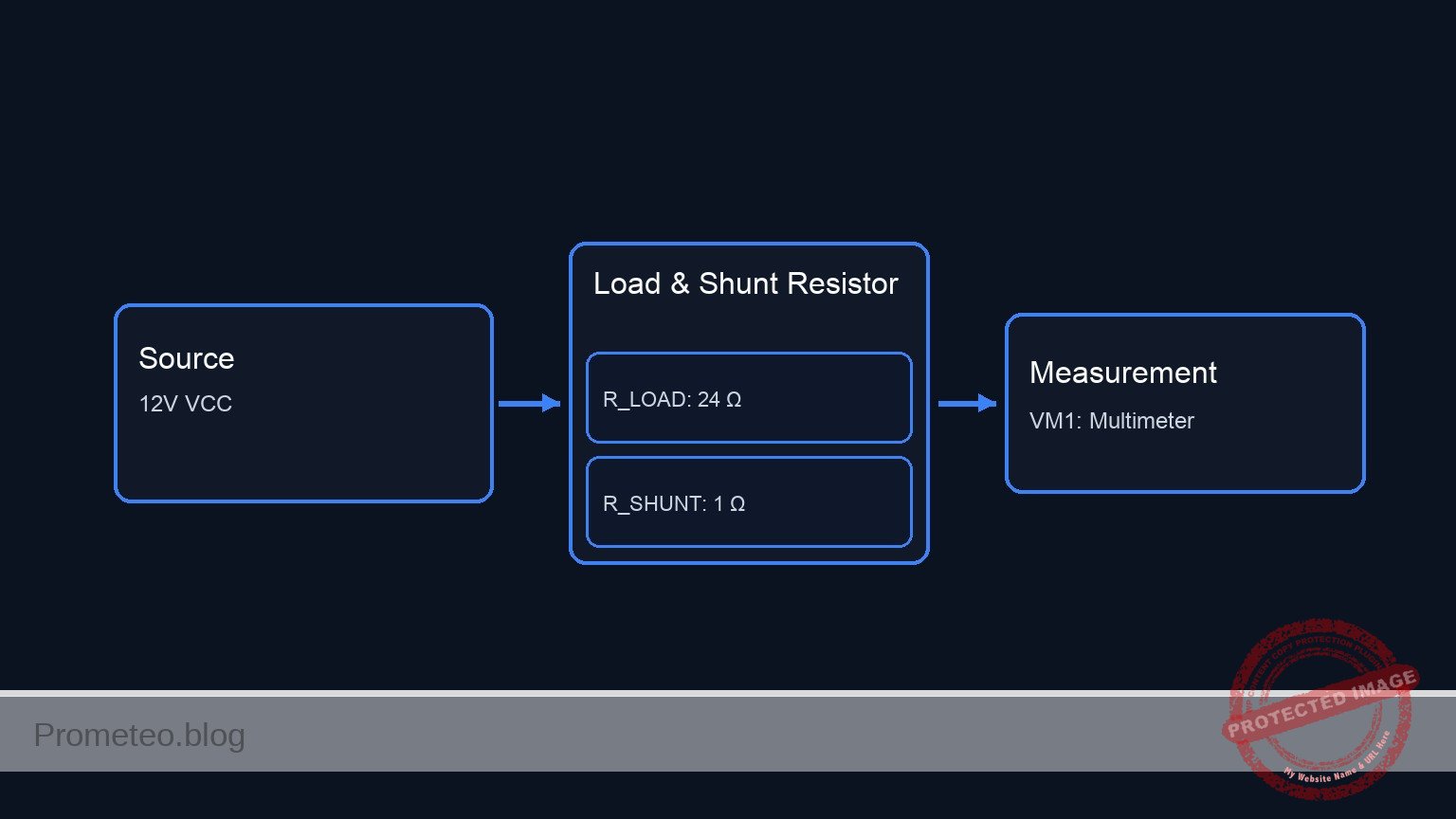
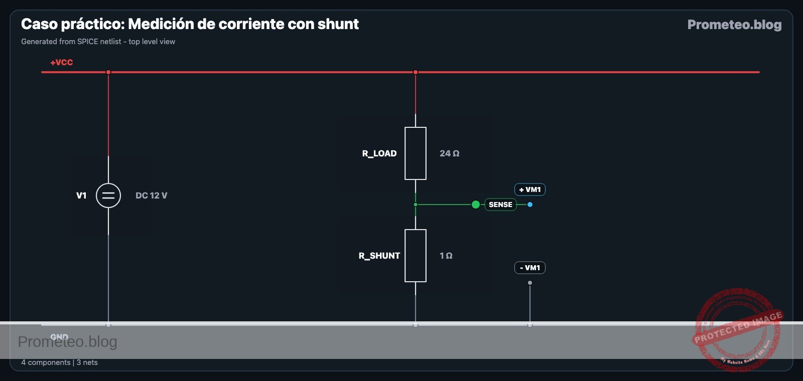
  • V1: fuente de alimentación de 12 V CC, función: fuente de energía principal
  • R_LOAD: resistencia de 24 Ω (10 W), función: carga principal de CC
  • R_SHUNT: resistencia de 1 Ω (1 W), función: shunt detector de corriente
  • VM1: Multímetro digital, función: medir la caída de tensión a través del shunt

Guía de conexionado

  • V1: conecta el terminal positivo al nodo VCC y el terminal negativo al nodo 0 (GND).
  • R_LOAD: se conecta entre el nodo VCC y el nodo SENSE.
  • R_SHUNT: se conecta entre el nodo SENSE y el nodo 0 (GND).
  • VM1: conecta la sonda positiva al nodo SENSE y la sonda negativa al nodo 0 (GND) para medir la caída de tensión a través del shunt.

Diagrama de bloques conceptual

Conceptual block diagram — Load & Shunt Resistor
Lectura rápida: entradas → bloque principal → salida (actuador o medida). Resume el esquemático ASCII de la siguiente sección.

Esquemático

[ V1: 12 V VCC ] --> [ R_LOAD: 24 Ω ] --(Node SENSE)--> [ R_SHUNT: 1 Ω ] --> GND
                                           |
                                           +--(+ probe)--> [ VM1: Multimeter ] --(- probe)--> GND
Esquema Eléctrico

Diagrama eléctrico

Diagrama eléctrico de medición de corriente con shunt
Generado desde la netlist SPICE validada del caso.

🔒 Este diagrama eléctrico es premium. Con el pase de 7 días o la suscripción mensual podrás desbloquear el material didáctico completo y el pack PDF listo para imprimir.🔓 Ver planes de acceso premium

Mediciones y pruebas

  1. Verificar la fuente de alimentación: Encienda V1 y mida la tensión en el nodo VCC con respecto al nodo 0. Debería leer exactamente 12 V.
  2. Medir la tensión del shunt (Vshunt): Configure su multímetro en el rango de milivoltios o voltios de CC. Mida la tensión en el nodo SENSE con respecto al nodo 0. Con una carga de 24 Ω y un shunt de 1 Ω (25 Ω en total), debería medir aproximadamente 480 mV (0.48 V).
  3. Calcular la corriente: Utilice la ley de Ohm (I = Vshunt / Rshunt). Divida la medición de 0.48 V por 1 Ω. La corriente total que fluye por el circuito es de 480 mA (0.48 A).
  4. Calcular la disipación de potencia: Calcule la potencia disipada por el shunt usando P = Vshunt × I. En este caso, 0.48 V × 0.48 A = 0.23 W. Debido a que seleccionamos una resistencia de 1 W, está operando de manera segura dentro de sus límites.
  5. Medir la caída de tensión de la carga: Mida la tensión entre el nodo VCC y el nodo SENSE. Debería ser aproximadamente 11.52 V, confirmando que el shunt «roba» muy poca tensión de la carga principal.

Netlist SPICE y simulación

Netlist SPICE de referencia (ngspice)

* Practical case: Current measurement with shunt
.width out=256

* Main power source
V1 VCC 0 DC 12

* Primary DC load
R_LOAD VCC SENSE 24

* Current sensing shunt
R_SHUNT SENSE 0 1

* Simulation commands
.op
.tran 1u 100u

* Print the input voltage and the voltage drop across the shunt (VM1)
.print tran V(VCC) V(SENSE)

.end

Copia este contenido en un archivo .cir y ejecútalo con ngspice.

Resultados de Simulación (Transitorio)

Resultados de Simulación (Transitorio)

Análisis: The simulation shows a constant 12V supply at VCC and a constant 0.48V at the SENSE node. This perfectly matches the theoretical voltage divider calculation (12V * 1Ω / 25Ω = 0.48V), indicating a current of 0.48A.
Show raw data table (108 rows)
Index   time            v(vcc)          v(sense)
0	0.000000e+00	1.200000e+01	4.800000e-01
1	1.000000e-08	1.200000e+01	4.800000e-01
2	2.000000e-08	1.200000e+01	4.800000e-01
3	4.000000e-08	1.200000e+01	4.800000e-01
4	8.000000e-08	1.200000e+01	4.800000e-01
5	1.600000e-07	1.200000e+01	4.800000e-01
6	3.200000e-07	1.200000e+01	4.800000e-01
7	6.400000e-07	1.200000e+01	4.800000e-01
8	1.280000e-06	1.200000e+01	4.800000e-01
9	2.280000e-06	1.200000e+01	4.800000e-01
10	3.280000e-06	1.200000e+01	4.800000e-01
11	4.280000e-06	1.200000e+01	4.800000e-01
12	5.280000e-06	1.200000e+01	4.800000e-01
13	6.280000e-06	1.200000e+01	4.800000e-01
14	7.280000e-06	1.200000e+01	4.800000e-01
15	8.280000e-06	1.200000e+01	4.800000e-01
16	9.280000e-06	1.200000e+01	4.800000e-01
17	1.028000e-05	1.200000e+01	4.800000e-01
18	1.128000e-05	1.200000e+01	4.800000e-01
19	1.228000e-05	1.200000e+01	4.800000e-01
20	1.328000e-05	1.200000e+01	4.800000e-01
21	1.428000e-05	1.200000e+01	4.800000e-01
22	1.528000e-05	1.200000e+01	4.800000e-01
23	1.628000e-05	1.200000e+01	4.800000e-01
... (84 more rows) ...

Errores comunes y cómo evitarlos

  • Usar un shunt con demasiada resistencia: Si el valor del shunt es demasiado alto (ej. 100 Ω), crea una «tensión de carga» (burden voltage) masiva, privando a la carga real de energía y alterando el comportamiento del circuito. Utilice siempre valores bajos (típicamente 1 Ω, 0.1 Ω, o incluso miliohmios).
  • Ignorar la potencia nominal del shunt: Una resistencia que reduce incluso una fracción de voltio puede disipar un calor sustancial si la corriente es alta. Calcule siempre P = I^2 × R y seleccione una resistencia con el doble de la potencia calculada.
  • Medir la corriente directamente a través del shunt: Configurar el multímetro en modo «Amperios» y ponerlo en paralelo con el shunt provocará un cortocircuito en el shunt, lo que podría fundir el fusible interno del multímetro. Utilice siempre el modo «Voltaje» para medir la caída de tensión a través del shunt.

Solución de problemas

  • Síntoma: El multímetro lee 0 V a través del shunt.
    • Causa: El circuito está abierto; la energía no llega a la carga o R_SHUNT está en cortocircuito.
    • Solución: Compruebe la continuidad de todos los cables, asegúrese de que la fuente de alimentación esté encendida y confirme que la carga esté conectada correctamente.
  • Síntoma: La resistencia shunt humea o se calienta peligrosamente.
    • Causa: La corriente excede la potencia nominal del shunt, o R_LOAD ha sido puenteada (creando un cortocircuito directo a través del shunt).
    • Solución: Apague la alimentación inmediatamente. Verifique que R_LOAD no esté puenteada y reemplace el shunt por uno de mayor potencia nominal si es necesario.
  • Síntoma: La corriente calculada parece mucho menor que el consumo esperado de la carga.
    • Causa: La resistencia de los cables de conexión o los contactos de la protoboard actúan como un shunt secundario no medido, sumándose a la resistencia total del circuito.
    • Solución: Asegúrese de utilizar cables cortos y gruesos para las conexiones de alimentación. Considere cambiar a una configuración de medición de 4 hilos (Kelvin) para obtener una precisión extrema.

Posibles mejoras y extensiones

  • Añadir un amplificador detector de corriente: Conecte un amplificador operacional (Op-Amp) a través de R_SHUNT en una configuración no inversora para amplificar la pequeña señal de milivoltios y convertirla en una señal robusta de 0-5 V fácilmente legible por el ADC de un microcontrolador.
  • Implementar medición de lado alto (high-side): Mueva R_SHUNT al «lado alto» (entre VCC y R_LOAD). Utilice un CI dedicado a la detección de corriente de lado alto (como el INA219) para medir la tensión diferencial, demostrando que la corriente se puede medir antes de que llegue a la carga mientras se mantiene la carga estrictamente conectada a tierra.

Más Casos Prácticos en Prometeo.blog

Encuentra este producto y/o libros sobre este tema en Amazon

Ir a Amazon

Como afiliado de Amazon, gano con las compras que cumplan los requisitos. Si compras a través de este enlace, ayudas a mantener este proyecto.

Quiz rápido

Pregunta 1: ¿Cuál es el objetivo principal de utilizar una resistencia shunt en el circuito descrito?


Pregunta 2: ¿Qué ley se utiliza para calcular la corriente total del circuito al medir la caída de tensión en el shunt?


Pregunta 3: ¿Cómo debe ser el valor de la resistencia shunt utilizada para este propósito?


Pregunta 4: ¿Por qué el uso de un shunt hace más segura la medición de alta corriente?


Pregunta 5: ¿Qué ventaja ofrece el shunt para la monitorización continua del consumo de energía?


Pregunta 6: ¿Cómo contribuye el shunt a la protección contra sobrecorriente?


Pregunta 7: ¿Qué problema de medición se minimiza al personalizar el tamaño del shunt?


Pregunta 8: ¿En qué tipo de circuito se centra el caso de uso descrito en el texto?


Pregunta 9: ¿Cómo se conecta la resistencia shunt respecto a la carga principal (dummy load) para medir la corriente total?


Pregunta 10: ¿Qué dispositivos menciona el texto que pueden aprovechar el shunt para realizar un seguimiento constante del consumo?


Carlos Núñez Zorrilla
Electronics & Computer Engineer

Ingeniero Superior en Electrónica de Telecomunicaciones e Ingeniero en Informática (titulaciones oficiales en España).

Sígueme:


Practical case: Current measurement with shunt

Current measurement with shunt prototype (Maker Style)

Level: Medium – Use a very low-value resistor to indirectly measure a DC load’s current via voltage drop.

Objective and use case

You will build a direct current (DC) circuit featuring a primary dummy load and a low-value series resistor, known as a shunt. By measuring the tiny voltage drop across this shunt, you will indirectly calculate the total current flowing through the circuit using Ohm’s Law.

Why this is useful:
* Safe high-current measurement: Avoids running massive currents directly through your multimeter’s internal, potentially fragile, circuitry.
* Continuous monitoring: Allows microcontrollers or analog panels to constantly track power consumption without breaking the circuit.
* Overcurrent protection: Provides a proportional voltage signal that can trigger a shutdown mechanism if the current exceeds safe limits.
* Lowering burden voltage: Customizing the shunt size minimizes the interference the measurement instrument imposes on the operating circuit.

Expected outcome:
* You will generate a measurable millivolt-range voltage drop across the low-side shunt resistor.
* You will correctly calculate the load current ($I = V/R$) from the observed voltage.
* You will verify the power dissipation (P = I^2 × R) of the shunt to ensure it operates within safe thermal limits.

Target audience and level: Intermediate electronics students learning indirect measurement techniques and power calculations.

Materials

  • V1: 12 V DC supply, function: main power source
  • R_LOAD: 24 Ω resistor (10 W), function: primary DC load
  • R_SHUNT: 1 Ω resistor (1 W), function: current sensing shunt
  • VM1: Digital Multimeter, function: measure voltage drop across shunt

Wiring guide

  • V1: connects positive terminal to node VCC and negative terminal to node 0 (GND).
  • R_LOAD: connects between node VCC and node SENSE.
  • R_SHUNT: connects between node SENSE and node 0 (GND).
  • VM1: connects positive probe to node SENSE and negative probe to node 0 (GND) to measure the voltage drop across the shunt.

Conceptual block diagram

Conceptual block diagram — Load & Shunt Resistor
Quick read: inputs → main block → output (actuator or measurement). This summarizes the ASCII schematic below.

Schematic

[ V1: 12 V VCC ] --> [ R_LOAD: 24 Ω ] --(Node SENSE)--> [ R_SHUNT: 1 Ω ] --> GND
                                           |
                                           +--(+ probe)--> [ VM1: Multimeter ] --(- probe)--> GND
Electrical Schematic

Electrical diagram

Electrical diagram for current measurement with shunt
Generated from the validated SPICE netlist for this case.

🔒 This electrical diagram is premium. With the 7-day pass or the monthly membership you can unlock the complete didactic material and the print-ready PDF pack.🔓 See premium access plans

Measurements and tests

  1. Verify the power supply: Turn on V1 and measure the voltage at node VCC relative to node 0. It should read exactly 12 V.
  2. Measure the shunt voltage (Vshunt): Set your multimeter to the DC millivolts or volts range. Measure the voltage at node SENSE relative to node 0. With a 24 Ω load and a 1 Ω shunt (25 Ω total), you should measure approximately 480 mV (0.48 V).
  3. Calculate the current: Use Ohm’s law (I = Vshunt / Rshunt). Divide the 0.48 V measurement by 1 Ω. The total current flowing through the circuit is 480 mA (0.48 A).
  4. Calculate power dissipation: Calculate the power dissipated by the shunt using P = Vshunt × I. In this case, 0.48 V × 0.48 A = 0.23 W. Because we selected a 1 W resistor, it is operating safely within its limits.
  5. Measure load voltage drop: Measure the voltage between node VCC and node SENSE. It should be approximately 11.52 V, confirming that the shunt «steals» very little voltage from the primary load.

SPICE netlist and simulation

Reference SPICE Netlist (ngspice)

* Practical case: Current measurement with shunt
.width out=256

* Main power source
V1 VCC 0 DC 12

* Primary DC load
R_LOAD VCC SENSE 24

* Current sensing shunt
R_SHUNT SENSE 0 1

* Simulation commands
.op
.tran 1u 100u

* Print the input voltage and the voltage drop across the shunt (VM1)
.print tran V(VCC) V(SENSE)

.end

Copy this content into a .cir file and run with ngspice.

Simulation Results (Transient Analysis)

Simulation Results (Transient Analysis)

Analysis: The simulation shows a constant 12V supply at VCC and a constant 0.48V at the SENSE node. This perfectly matches the theoretical voltage divider calculation (12V * 1Ω / 25Ω = 0.48V), indicating a current of 0.48A.
Show raw data table (108 rows)
Index   time            v(vcc)          v(sense)
0	0.000000e+00	1.200000e+01	4.800000e-01
1	1.000000e-08	1.200000e+01	4.800000e-01
2	2.000000e-08	1.200000e+01	4.800000e-01
3	4.000000e-08	1.200000e+01	4.800000e-01
4	8.000000e-08	1.200000e+01	4.800000e-01
5	1.600000e-07	1.200000e+01	4.800000e-01
6	3.200000e-07	1.200000e+01	4.800000e-01
7	6.400000e-07	1.200000e+01	4.800000e-01
8	1.280000e-06	1.200000e+01	4.800000e-01
9	2.280000e-06	1.200000e+01	4.800000e-01
10	3.280000e-06	1.200000e+01	4.800000e-01
11	4.280000e-06	1.200000e+01	4.800000e-01
12	5.280000e-06	1.200000e+01	4.800000e-01
13	6.280000e-06	1.200000e+01	4.800000e-01
14	7.280000e-06	1.200000e+01	4.800000e-01
15	8.280000e-06	1.200000e+01	4.800000e-01
16	9.280000e-06	1.200000e+01	4.800000e-01
17	1.028000e-05	1.200000e+01	4.800000e-01
18	1.128000e-05	1.200000e+01	4.800000e-01
19	1.228000e-05	1.200000e+01	4.800000e-01
20	1.328000e-05	1.200000e+01	4.800000e-01
21	1.428000e-05	1.200000e+01	4.800000e-01
22	1.528000e-05	1.200000e+01	4.800000e-01
23	1.628000e-05	1.200000e+01	4.800000e-01
... (84 more rows) ...

Common mistakes and how to avoid them

  • Using a shunt with too much resistance: If the shunt value is too high (e.g., 100 Ω), it creates a massive «burden voltage,» starving the actual load of power and altering the circuit’s behavior. Always use low values (typically 1 Ω, 0.1 Ω, or even milliohms).
  • Ignoring the power rating of the shunt: A resistor dropping even a fraction of a volt can dissipate substantial heat if the current is high. Always calculate P = I^2 × R and select a resistor with double the calculated wattage rating.
  • Measuring current directly across the shunt: Setting the multimeter to «Amps» mode and putting it in parallel with the shunt will short out the shunt, potentially blowing the multimeter’s internal fuse. Always use the «Voltage» mode to measure the voltage drop across the shunt.

Troubleshooting

  • Symptom: Multimeter reads 0 V across the shunt.
    • Cause: The circuit is open; power isn’t reaching the load, or R_SHUNT is shorted out.
    • Fix: Check all wire continuity, ensure the power supply is turned on, and confirm the load is properly connected.
  • Symptom: The shunt resistor is smoking or gets dangerously hot.
    • Cause: The current exceeds the wattage rating of the shunt, or R_LOAD has been bypassed (creating a short circuit directly through the shunt).
    • Fix: Immediately turn off the power. Verify R_LOAD is not bypassed and replace the shunt with one of a higher wattage rating if necessary.
  • Symptom: The calculated current seems far lower than the expected load consumption.
    • Cause: The resistance of the connecting wires or breadboard contacts is acting as an unmeasured secondary shunt, adding to the total circuit resistance.
    • Fix: Ensure short, thick wires are used for power connections. Consider switching to a 4-wire (Kelvin) measurement setup for extreme precision.

Possible improvements and extensions

  • Add a current-sense amplifier: Connect an Operational Amplifier (Op-Amp) across R_SHUNT in a non-inverting configuration to amplify the small millivolt signal into a robust 0-5 V signal easily readable by a microcontroller’s ADC.
  • Implement high-side sensing: Move R_SHUNT to the «high side» (between VCC and R_LOAD). Use a dedicated high-side current sensing IC (such as the INA219) to measure the differential voltage, proving that current can be measured before it reaches the load while keeping the load strictly grounded.

More Practical Cases on Prometeo.blog

Find this product and/or books on this topic on Amazon

Go to Amazon

As an Amazon Associate, I earn from qualifying purchases. If you buy through this link, you help keep this project running.

Quick Quiz

Question 1: What is the primary purpose of the low-value series resistor (shunt) in this circuit?


Question 2: Which formula is used to calculate the load current from the observed voltage drop across the shunt?


Question 3: How does using a shunt resistor help with safe high-current measurements?


Question 4: What is one benefit of using a shunt resistor for continuous monitoring?


Question 5: How can a shunt resistor assist in overcurrent protection?


Question 6: Why is customizing the shunt size important for the operating circuit?


Question 7: What range of voltage drop is expected across the low-side shunt resistor?


Question 8: What type of circuit is being built in this scenario?


Question 9: What is another name for the low-value series resistor used to measure current?


Question 10: What physical principle is used to calculate the total current flowing through the circuit in this setup?


Carlos Núñez Zorrilla
Electronics & Computer Engineer

Telecommunications Electronics Engineer and Computer Engineer (official degrees in Spain).

Follow me:


Practical case: Base Biasing with Resistor

Base Biasing with Resistor prototype (Maker Style)

Level: Medium — Calculate and verify a base resistor to switch an NPN transistor safely from a logic output.

Objective and use case

You will build a simple transistor switch where a 5 V logic output drives an NPN transistor through a base resistor. The goal is to choose the resistor so the transistor turns the load on reliably without exceeding the allowed logic output current.

Why it is useful:
– To drive a relay module, buzzer, or small lamp from a microcontroller pin.
– To control loads that require more current than a logic output can supply directly.
– To protect a logic output from excessive base current.
– To learn how to verify transistor saturation with real voltage and current measurements.

Expected outcome:
– When the logic output is LOW, the transistor remains OFF and the load is de-energized.
– When the logic output is HIGH, the transistor turns ON and the load current is about 20 mA.
– Base current stays below the logic output limit, target about 4.3 mA.
– Measured base-emitter voltage is about 0.7 V when ON.
– Measured collector-emitter voltage is low in saturation, typically below 0.2 V.

Target audience and level: Students with basic DC circuit and transistor knowledge.

Materials

  • V1: 5 V DC supply
  • VSIG: 0 V / 5 V logic source, function: control signal for transistor base
  • R1: 1 kΩ resistor, function: base current limiting
  • R2: 150 Ω resistor, function: load current limiting for LED branch
  • D1: red LED, function: visible collector load indicator
  • Q1: 2N2222 NPN transistor, function: low-side switch
  • M1: digital multimeter, function: voltage and current measurements
  • M2: optional second multimeter, function: simultaneous current check

Wiring guide

Use these node names: VCC, 0, VIN, VB, VC.

  • V1 connects between VCC and 0.
  • VSIG connects between VIN and 0.
  • R1 connects between VIN and VB.
  • Q1 collector connects to VC.
  • Q1 base connects to VB.
  • Q1 emitter connects to 0.
  • R2 connects between VCC and the anode node of D1.
  • D1 anode connects to R2; D1 cathode connects to VC.

Practical design values:
– Load current target: about Ic = (5 V - 2.0 V - 0.2 V) / 150 Ω ≈ 18.7 mA
– Forced gain for saturation: use β_forced ≈ 10
– Required base current: Ib ≈ Ic / 10 ≈ 1.9 mA
– Base resistor estimate: R1 ≈ (5 V - 0.7 V) / 1.9 mA ≈ 2.26 kΩ

To make switching more robust, choose a lower standard value:
– Selected R1 = 1 kΩ
– Expected base current: Ib ≈ (5 V - 0.7 V) / 1 kΩ ≈ 4.3 mA

This value is suitable only if the logic output can safely source at least 4.3 mA.

Conceptual block diagram

Conceptual block diagram — Base-biased NPN switch
Quick read: inputs → main block → output (actuator or measurement). This summarizes the ASCII schematic below.

Schematic

Practical case: Base Biasing with Resistor

Power / load path:
[ V1: 5 V DC Supply ] --(VCC)--> [ R2: 150 ohm ] --(LED current limit)--> [ D1: Red LED ] --(cathode at VC)--> [ Q1:C 2N2222 ]
[ Q1:C 2N2222 ] --(collector-emitter path)--> [ Q1:E 2N2222 ] --(0 / GND)--> [ V1: 0 V ]

Control / base path:
[ VSIG: 0/5 V Logic Source ] --(VIN)--> [ R1: 1 kohm ] --(VB)--> [ Q1:B 2N2222 ]
[ Q1:B 2N2222 ] --(base-emitter junction)--> [ Q1:E 2N2222 ] --(0 / GND)--> [ VSIG: 0 V ]

Node labels:
[ VIN ] --> [ R1 ] --> [ VB ] --> [ Q1:B ]
[ VCC ] --> [ R2 ] --> [ D1 Anode ]
[ D1 Cathode ] --> [ VC ] --> [ Q1:C ]
[ Q1:E ] --> [ 0 / GND ]

Optional measurements:
[ M1 DMM ] --(measure V_B or V_C vs 0)--> [ VB / VC ] --> [ 0 / GND ]
[ M2 DMM ] --(current mode, inserted in series where needed)--> [ Base path or Load path ]
Electrical Schematic

Electrical diagram

Electrical diagram for Practical case: Base biasing with resistor
Generated from the validated SPICE netlist for this case.

🔒 This electrical diagram is premium. With the 7-day pass or the monthly membership you can unlock the complete didactic material and the print-ready PDF pack.🔓 See premium access plans

Measurements and tests

  1. Power-off check
  2. Verify all connections before applying power.
  3. Confirm Q1 emitter goes to 0.
  4. Confirm R1 is in series between VIN and VB.

  5. OFF-state test

  6. Set VSIG = 0 V.
  7. Measure Vb from VB to 0: expected near 0 V.
  8. Measure Vce from VC to 0: expected near 5 V.
  9. Observe D1: it should be OFF.
  10. Measure Ib: expected approximately 0 mA.
  11. Measure Ic: expected approximately 0 mA.

  12. ON-state test

  13. Set VSIG = 5 V.
  14. Measure Vb: expected about 0.7 V.
  15. Measure Vbe: expected about 0.65 V to 0.8 V.
  16. Measure Ib by placing the meter in series with R1: expected about 4.3 mA.
  17. Measure Vc: expected low, typically below 0.2 V to 0.3 V.
  18. Measure Vce: expected below 0.2 V if saturation is achieved.
  19. Measure Ic in series with the collector path: expected about 18 mA to 20 mA.
  20. Observe D1: it should be clearly ON.

  21. Logic output safety check

  22. Compare the measured Ib with the maximum source current allowed by the logic output.
  23. If the logic output rating is less than the measured base current, increase R1.

  24. Verification calculation

  25. Compute measured gain in switching mode: Ic / Ib.
  26. Example with measured values: 19 mA / 4.3 mA ≈ 4.4
  27. This is consistent with saturated switching, where the transistor is intentionally overdriven.

  28. Pass criteria

  29. Ib does not exceed the logic output limit.
  30. D1 turns fully ON at logic HIGH and fully OFF at logic LOW.
  31. Vce in ON state is low enough to confirm saturation.

SPICE netlist and simulation

Reference SPICE Netlist (ngspice) — excerptFull SPICE netlist (ngspice)

* Practical case: Base Biasing with Resistor
.width out=256

V1 VCC 0 DC 5
VSIG VIN 0 PULSE(0 5 10m 1u 1u 245m 1s)

R1 VIN VB 1k
R2 VCC VLED 150
D1 VLED VC DRED
Q1 VC VB 0 Q2N2222

* Optional multimeter loading approximations (high impedance voltmeters)
RM1 VC 0 10Meg
RM2 VB 0 10Meg

* Alias nodes for guaranteed logging
VALIASIN IN VIN 0
VALIASOUT OUT VC 0

.model DRED D(IS=1e-18 N=2.0 RS=10 CJO=20p VJ=0.75 M=0.5 TT=50n BV=5 IBV=10u)
* ... (truncated in public view) ...

Copy this content into a .cir file and run with ngspice.

🔒 Part of this section is premium. With the 7-day pass or the monthly membership you can access the full content (materials, wiring, detailed build, validation, troubleshooting, variants and checklist) and download the complete print-ready PDF pack.

* Practical case: Base Biasing with Resistor
.width out=256

V1 VCC 0 DC 5
VSIG VIN 0 PULSE(0 5 10m 1u 1u 245m 1s)

R1 VIN VB 1k
R2 VCC VLED 150
D1 VLED VC DRED
Q1 VC VB 0 Q2N2222

* Optional multimeter loading approximations (high impedance voltmeters)
RM1 VC 0 10Meg
RM2 VB 0 10Meg

* Alias nodes for guaranteed logging
VALIASIN IN VIN 0
VALIASOUT OUT VC 0

.model DRED D(IS=1e-18 N=2.0 RS=10 CJO=20p VJ=0.75 M=0.5 TT=50n BV=5 IBV=10u)
.model Q2N2222 NPN(IS=1e-14 BF=200 VAF=100 IKF=0.1 ISE=1e-13 NE=1.5 BR=5 NR=1.0 VAR=25 IKR=0.05
+ RC=0.5 RE=0.2 RB=10 CJE=25p VJE=0.75 MJE=0.33 TF=0.4n XTF=2 CJC=8p VJC=0.55 MJC=0.33 TR=50n)

.save V(IN) V(OUT) V(VIN) V(VC) V(VB) V(VLED) I(V1) I(VSIG)

.op
.print op V(IN) V(OUT) V(VIN) V(VC) V(VB) V(VLED) I(V1) I(VSIG)

.tran 0.1m 250m
.print tran V(IN) V(OUT) V(VIN) V(VC) V(VB) V(VLED) I(V1) I(VSIG)

.end

Simulation Results (Transient Analysis)

Simulation Results (Transient Analysis)
Show raw data table (2528 rows)
Index   time            v(in)           v(out)          v(vin)          v(vc)           v(vb)           v(vled)         v1#branch       vsig#branch
0	0.000000e+00	0.000000e+00	3.623103e+00	0.000000e+00	3.623103e+00	3.624741e-09	4.999946e+00	-3.62318e-07	3.624741e-12
1	1.000000e-06	0.000000e+00	3.623104e+00	0.000000e+00	3.623104e+00	6.699379e-09	4.999946e+00	-3.62321e-07	6.699379e-12
2	2.000000e-06	0.000000e+00	3.623105e+00	0.000000e+00	3.623105e+00	6.506970e-09	4.999946e+00	-3.62321e-07	6.506970e-12
3	4.000000e-06	0.000000e+00	3.623106e+00	0.000000e+00	3.623106e+00	5.984372e-09	4.999946e+00	-3.62320e-07	5.984372e-12
4	8.000000e-06	0.000000e+00	3.623108e+00	0.000000e+00	3.623108e+00	5.188535e-09	4.999946e+00	-3.62320e-07	5.188535e-12
5	1.600000e-05	0.000000e+00	3.623110e+00	0.000000e+00	3.623110e+00	4.293865e-09	4.999946e+00	-3.62319e-07	4.293865e-12
6	3.200000e-05	0.000000e+00	3.623112e+00	0.000000e+00	3.623112e+00	3.693772e-09	4.999946e+00	-3.62318e-07	3.693772e-12
7	6.400000e-05	0.000000e+00	3.623112e+00	0.000000e+00	3.623112e+00	3.610539e-09	4.999946e+00	-3.62318e-07	3.610539e-12
8	1.280000e-04	0.000000e+00	3.623112e+00	0.000000e+00	3.623112e+00	3.631021e-09	4.999946e+00	-3.62318e-07	3.631021e-12
9	2.280000e-04	0.000000e+00	3.623112e+00	0.000000e+00	3.623112e+00	3.621414e-09	4.999946e+00	-3.62318e-07	3.621414e-12
10	3.280000e-04	0.000000e+00	3.623112e+00	0.000000e+00	3.623112e+00	3.626121e-09	4.999946e+00	-3.62318e-07	3.626121e-12
11	4.280000e-04	0.000000e+00	3.623112e+00	0.000000e+00	3.623112e+00	3.624676e-09	4.999946e+00	-3.62318e-07	3.624676e-12
12	5.280000e-04	0.000000e+00	3.623112e+00	0.000000e+00	3.623112e+00	3.623957e-09	4.999946e+00	-3.62318e-07	3.623957e-12
13	6.280000e-04	0.000000e+00	3.623112e+00	0.000000e+00	3.623112e+00	3.626113e-09	4.999946e+00	-3.62318e-07	3.626113e-12
14	7.280000e-04	0.000000e+00	3.623112e+00	0.000000e+00	3.623112e+00	3.623011e-09	4.999946e+00	-3.62318e-07	3.623011e-12
15	8.280000e-04	0.000000e+00	3.623112e+00	0.000000e+00	3.623112e+00	3.626745e-09	4.999946e+00	-3.62318e-07	3.626745e-12
16	9.280000e-04	0.000000e+00	3.623112e+00	0.000000e+00	3.623112e+00	3.622584e-09	4.999946e+00	-3.62318e-07	3.622584e-12
17	1.028000e-03	0.000000e+00	3.623112e+00	0.000000e+00	3.623112e+00	3.627045e-09	4.999946e+00	-3.62318e-07	3.627045e-12
18	1.128000e-03	0.000000e+00	3.623112e+00	0.000000e+00	3.623112e+00	3.622367e-09	4.999946e+00	-3.62318e-07	3.622367e-12
19	1.228000e-03	0.000000e+00	3.623112e+00	0.000000e+00	3.623112e+00	3.627168e-09	4.999946e+00	-3.62318e-07	3.627168e-12
20	1.328000e-03	0.000000e+00	3.623112e+00	0.000000e+00	3.623112e+00	3.622305e-09	4.999946e+00	-3.62318e-07	3.622305e-12
21	1.428000e-03	0.000000e+00	3.623112e+00	0.000000e+00	3.623112e+00	3.627229e-09	4.999946e+00	-3.62318e-07	3.627229e-12
22	1.528000e-03	0.000000e+00	3.623112e+00	0.000000e+00	3.623112e+00	3.622257e-09	4.999946e+00	-3.62318e-07	3.622257e-12
23	1.628000e-03	0.000000e+00	3.623112e+00	0.000000e+00	3.623112e+00	3.627228e-09	4.999946e+00	-3.62318e-07	3.627228e-12
... (2504 more rows) ...

Common mistakes and how to avoid them

  1. Using no base resistor
  2. Error: connecting the logic output directly to the transistor base.
  3. Result: excessive base current and possible damage to the logic output.
  4. Fix: always place R1 between VIN and VB.

  5. Choosing a base resistor that is too large

  6. Error: using R1 = 10 kΩ without checking current.
  7. Result: base current may be too low, so the transistor may not saturate.
  8. Fix: calculate Ib from the load current and use a forced gain of about 10 for switching.

  9. Reversing transistor terminals

  10. Error: swapping collector and emitter.
  11. Result: abnormal voltages, weak load current, or no switching.
  12. Fix: confirm the 2N2222 pinout from its datasheet before wiring.

Troubleshooting

  • Symptom: LED never turns ON
  • Cause: VSIG is not reaching 5 V, or Q1 base is not connected through R1.
  • Fix: measure VIN and VB; verify R1 continuity and transistor pinout.

  • Symptom: LED is dim

  • Cause: transistor is not saturated because R1 is too large.
  • Fix: reduce R1 after checking the logic output current limit.

  • Symptom: Logic output voltage drops when ON

  • Cause: base current demand is too high for the logic source.
  • Fix: increase R1 or use a transistor driver stage.

  • Symptom: LED stays ON all the time

  • Cause: wrong wiring at the collector node or unintended base bias.
  • Fix: check that Q1 emitter is at 0 and that VIN actually goes to 0 V in the LOW state.

  • Symptom: Measured Vce is high when ON

  • Cause: insufficient base current or incorrect collector load wiring.
  • Fix: verify Ib, recalculate R1, and check R2 and D1 orientation.

Possible improvements and extensions

  • Add a 10 kΩ pull-down resistor from VB to 0 so the transistor stays OFF if the logic source becomes disconnected or high-impedance.
  • Replace the LED load with a relay coil and add a flyback diode across the coil to study transistor switching with inductive loads.

More Practical Cases on Prometeo.blog

Find this product and/or books on this topic on Amazon

Go to Amazon

As an Amazon Associate, I earn from qualifying purchases. If you buy through this link, you help keep this project running.

Quick Quiz

Question 1: What is the main purpose of the base resistor in the 5 V logic-driven NPN switch?


Question 2: According to the article, what load current is expected when the transistor is ON?


Question 3: What is the target base current mentioned for reliable switching?


Question 4: If the logic output is HIGH at 5 V and the base-emitter voltage is about 0.7 V, what voltage is approximately across the 1 kΩ base resistor?


Question 5: Using the article values, what base current flows through a 1 kΩ resistor when driven from 5 V with V_BE about 0.7 V?


Question 6: Why is a forced beta of around 5 reasonable here?


Question 7: What collector-emitter voltage indicates the transistor is in saturation according to the article?


Question 8: What should happen when the logic output is LOW?


Question 9: Which transistor is used as the low-side switch in this example?


Question 10: If a microcontroller pin can safely supply up to 5 mA, is the article's target base current acceptable?


Carlos Núñez Zorrilla
Electronics & Computer Engineer

Telecommunications Electronics Engineer and Computer Engineer (official degrees in Spain).

Follow me:


Caso práctico: Polarización de base con resistor

Prototipo de Polarización de base con resistor (Maker Style)

Nivel: Medio — Calcular y verificar un resistor de base para conmutar de forma segura un transistor NPN desde una salida lógica.

Objetivo y caso de uso

Construirás un interruptor simple con transistor donde una salida lógica de 5 V controla un transistor NPN a través de un resistor de base. El objetivo es elegir el resistor para que el transistor encienda la carga de forma fiable sin exceder la corriente permitida de la salida lógica.

Por qué es útil:
– Para accionar un módulo de relé, zumbador o lámpara pequeña desde un pin de microcontrolador.
– Para controlar cargas que requieren más corriente de la que una salida lógica puede suministrar directamente.
– Para proteger una salida lógica de una corriente de base excesiva.
– Para aprender a verificar la saturación del transistor con mediciones reales de voltaje y corriente.

Resultado esperado:
– Cuando la salida lógica está en LOW, el transistor permanece en OFF y la carga queda desenergizada.
– Cuando la salida lógica está en HIGH, el transistor pasa a ON y la corriente de carga es de aproximadamente 20 mA.
– La corriente de base se mantiene por debajo del límite de la salida lógica, con un objetivo de aproximadamente 4.3 mA.
– El voltaje base-emisor medido es de aproximadamente 0.7 V cuando está en ON.
– El voltaje colector-emisor medido es bajo en saturación, típicamente por debajo de 0.2 V.

Público objetivo y nivel: Estudiantes con conocimientos básicos de circuitos de CC y transistores.

Materiales

  • V1: fuente de CC de 5 V
  • VSIG: fuente lógica de 0 V / 5 V, función: señal de control para la base del transistor
  • R1: resistor de 1 kΩ, función: limitación de corriente de base
  • R2: resistor de 150 Ω, función: limitación de corriente de carga para la rama del LED
  • D1: LED rojo, función: indicador visible de carga en el colector
  • Q1: transistor NPN 2N2222, función: interruptor low-side
  • M1: multímetro digital, función: mediciones de voltaje y corriente
  • M2: segundo multímetro opcional, función: comprobación simultánea de corriente

Guía de conexionado

Usa estos nombres de nodo: VCC, 0, VIN, VB, VC.

  • V1 se conecta entre VCC y 0.
  • VSIG se conecta entre VIN y 0.
  • R1 se conecta entre VIN y VB.
  • El colector de Q1 se conecta a VC.
  • La base de Q1 se conecta a VB.
  • El emisor de Q1 se conecta a 0.
  • R2 se conecta entre VCC y el nodo del ánodo de D1.
  • El ánodo de D1 se conecta a R2; el cátodo de D1 se conecta a VC.

Valores prácticos de diseño:
– Objetivo de corriente de carga: aproximadamente Ic = (5 V - 2.0 V - 0.2 V) / 150 Ω ≈ 18.7 mA
– Ganancia forzada para saturación: usar β_forced ≈ 10
– Corriente de base requerida: Ib ≈ Ic / 10 ≈ 1.9 mA
– Estimación del resistor de base: R1 ≈ (5 V - 0.7 V) / 1.9 mA ≈ 2.26 kΩ

Para hacer la conmutación más robusta, elige un valor estándar más bajo:
R1 seleccionado = 1 kΩ
– Corriente de base esperada: Ib ≈ (5 V - 0.7 V) / 1 kΩ ≈ 4.3 mA

Este valor solo es adecuado si la salida lógica puede suministrar con seguridad al menos 4.3 mA.

Diagrama de bloques conceptual

Conceptual block diagram — Base-biased NPN switch
Lectura rápida: entradas → bloque principal → salida (actuador o medida). Resume el esquemático ASCII de la siguiente sección.

Esquemático

Practical case: Base Biasing with Resistor

Power / load path:
[ V1: 5 V DC Supply ] --(VCC)--> [ R2: 150 ohm ] --(LED current limit)--> [ D1: Red LED ] --(cathode at VC)--> [ Q1:C 2N2222 ]
[ Q1:C 2N2222 ] --(collector-emitter path)--> [ Q1:E 2N2222 ] --(0 / GND)--> [ V1: 0 V ]

Control / base path:
[ VSIG: 0/5 V Logic Source ] --(VIN)--> [ R1: 1 kohm ] --(VB)--> [ Q1:B 2N2222 ]
[ Q1:B 2N2222 ] --(base-emitter junction)--> [ Q1:E 2N2222 ] --(0 / GND)--> [ VSIG: 0 V ]

Node labels:
[ VIN ] --> [ R1 ] --> [ VB ] --> [ Q1:B ]
[ VCC ] --> [ R2 ] --> [ D1 Anode ]
[ D1 Cathode ] --> [ VC ] --> [ Q1:C ]
[ Q1:E ] --> [ 0 / GND ]

Optional measurements:
[ M1 DMM ] --(measure V_B or V_C vs 0)--> [ VB / VC ] --> [ 0 / GND ]
[ M2 DMM ] --(current mode, inserted in series where needed)--> [ Base path or Load path ]
Esquema Eléctrico

Diagrama eléctrico

Diagrama eléctrico del caso práctico: Polarización de base con resistor
Generado desde la netlist SPICE validada del caso.

🔒 Este diagrama eléctrico es premium. Con el pase de 7 días o la suscripción mensual podrás desbloquear el material didáctico completo y el pack PDF listo para imprimir.🔓 Ver planes de acceso premium

Mediciones y pruebas

  1. Comprobación con alimentación apagada
  2. Verifica todas las conexiones antes de aplicar alimentación.
  3. Confirma que el emisor de Q1 va a 0.
  4. Confirma que R1 está en serie entre VIN y VB.

  5. Prueba en estado OFF

  6. Ajusta VSIG = 0 V.
  7. Mide Vb desde VB hasta 0: se espera cerca de 0 V.
  8. Mide Vce desde VC hasta 0: se espera cerca de 5 V.
  9. Observa D1: debe estar en OFF.
  10. Mide Ib: se espera aproximadamente 0 mA.
  11. Mide Ic: se espera aproximadamente 0 mA.

  12. Prueba en estado ON

  13. Ajusta VSIG = 5 V.
  14. Mide Vb: se espera aproximadamente 0.7 V.
  15. Mide Vbe: se espera aproximadamente entre 0.65 V y 0.8 V.
  16. Mide Ib colocando el medidor en serie con R1: se espera aproximadamente 4.3 mA.
  17. Mide Vc: se espera bajo, típicamente por debajo de 0.2 V a 0.3 V.
  18. Mide Vce: se espera por debajo de 0.2 V si se alcanza la saturación.
  19. Mide Ic en serie con la trayectoria del colector: se espera aproximadamente entre 18 mA y 20 mA.
  20. Observa D1: debe estar claramente en ON.

  21. Comprobación de seguridad de la salida lógica

  22. Compara la Ib medida con la corriente máxima de salida permitida por la salida lógica.
  23. Si la especificación de la salida lógica es menor que la corriente de base medida, aumenta R1.

  24. Cálculo de verificación

  25. Calcula la ganancia medida en modo de conmutación: Ic / Ib.
  26. Ejemplo con valores medidos: 19 mA / 4.3 mA ≈ 4.4
  27. Esto es consistente con conmutación en saturación, donde el transistor es sobreactivado intencionalmente.

  28. Criterios de aprobación

  29. Ib no excede el límite de la salida lógica.
  30. D1 se enciende completamente con lógica HIGH y se apaga completamente con lógica LOW.
  31. Vce en estado ON es lo bastante bajo como para confirmar saturación.

Netlist SPICE y simulación

Netlist SPICE de referencia (ngspice) — extractoNetlist SPICE completo (ngspice)

* Practical case: Base Biasing with Resistor
.width out=256

V1 VCC 0 DC 5
VSIG VIN 0 PULSE(0 5 10m 1u 1u 245m 1s)

R1 VIN VB 1k
R2 VCC VLED 150
D1 VLED VC DRED
Q1 VC VB 0 Q2N2222

* Optional multimeter loading approximations (high impedance voltmeters)
RM1 VC 0 10Meg
RM2 VB 0 10Meg

* Alias nodes for guaranteed logging
VALIASIN IN VIN 0
VALIASOUT OUT VC 0

.model DRED D(IS=1e-18 N=2.0 RS=10 CJO=20p VJ=0.75 M=0.5 TT=50n BV=5 IBV=10u)
* ... (truncated in public view) ...

Copia este contenido en un archivo .cir y ejecútalo con ngspice.

🔒 Parte del contenido de esta sección es premium. Con el pase de 7 días o la suscripción mensual tendrás acceso al contenido completo (materiales, conexionado, compilación detallada, validación paso a paso, troubleshooting, mejoras/variantes y checklist) y podrás descargar el pack PDF listo para imprimir.

* Practical case: Base Biasing with Resistor
.width out=256

V1 VCC 0 DC 5
VSIG VIN 0 PULSE(0 5 10m 1u 1u 245m 1s)

R1 VIN VB 1k
R2 VCC VLED 150
D1 VLED VC DRED
Q1 VC VB 0 Q2N2222

* Optional multimeter loading approximations (high impedance voltmeters)
RM1 VC 0 10Meg
RM2 VB 0 10Meg

* Alias nodes for guaranteed logging
VALIASIN IN VIN 0
VALIASOUT OUT VC 0

.model DRED D(IS=1e-18 N=2.0 RS=10 CJO=20p VJ=0.75 M=0.5 TT=50n BV=5 IBV=10u)
.model Q2N2222 NPN(IS=1e-14 BF=200 VAF=100 IKF=0.1 ISE=1e-13 NE=1.5 BR=5 NR=1.0 VAR=25 IKR=0.05
+ RC=0.5 RE=0.2 RB=10 CJE=25p VJE=0.75 MJE=0.33 TF=0.4n XTF=2 CJC=8p VJC=0.55 MJC=0.33 TR=50n)

.save V(IN) V(OUT) V(VIN) V(VC) V(VB) V(VLED) I(V1) I(VSIG)

.op
.print op V(IN) V(OUT) V(VIN) V(VC) V(VB) V(VLED) I(V1) I(VSIG)

.tran 0.1m 250m
.print tran V(IN) V(OUT) V(VIN) V(VC) V(VB) V(VLED) I(V1) I(VSIG)

.end

Resultados de Simulación (Transitorio)

Resultados de Simulación (Transitorio)
Show raw data table (2528 rows)
Index   time            v(in)           v(out)          v(vin)          v(vc)           v(vb)           v(vled)         v1#branch       vsig#branch
0	0.000000e+00	0.000000e+00	3.623103e+00	0.000000e+00	3.623103e+00	3.624741e-09	4.999946e+00	-3.62318e-07	3.624741e-12
1	1.000000e-06	0.000000e+00	3.623104e+00	0.000000e+00	3.623104e+00	6.699379e-09	4.999946e+00	-3.62321e-07	6.699379e-12
2	2.000000e-06	0.000000e+00	3.623105e+00	0.000000e+00	3.623105e+00	6.506970e-09	4.999946e+00	-3.62321e-07	6.506970e-12
3	4.000000e-06	0.000000e+00	3.623106e+00	0.000000e+00	3.623106e+00	5.984372e-09	4.999946e+00	-3.62320e-07	5.984372e-12
4	8.000000e-06	0.000000e+00	3.623108e+00	0.000000e+00	3.623108e+00	5.188535e-09	4.999946e+00	-3.62320e-07	5.188535e-12
5	1.600000e-05	0.000000e+00	3.623110e+00	0.000000e+00	3.623110e+00	4.293865e-09	4.999946e+00	-3.62319e-07	4.293865e-12
6	3.200000e-05	0.000000e+00	3.623112e+00	0.000000e+00	3.623112e+00	3.693772e-09	4.999946e+00	-3.62318e-07	3.693772e-12
7	6.400000e-05	0.000000e+00	3.623112e+00	0.000000e+00	3.623112e+00	3.610539e-09	4.999946e+00	-3.62318e-07	3.610539e-12
8	1.280000e-04	0.000000e+00	3.623112e+00	0.000000e+00	3.623112e+00	3.631021e-09	4.999946e+00	-3.62318e-07	3.631021e-12
9	2.280000e-04	0.000000e+00	3.623112e+00	0.000000e+00	3.623112e+00	3.621414e-09	4.999946e+00	-3.62318e-07	3.621414e-12
10	3.280000e-04	0.000000e+00	3.623112e+00	0.000000e+00	3.623112e+00	3.626121e-09	4.999946e+00	-3.62318e-07	3.626121e-12
11	4.280000e-04	0.000000e+00	3.623112e+00	0.000000e+00	3.623112e+00	3.624676e-09	4.999946e+00	-3.62318e-07	3.624676e-12
12	5.280000e-04	0.000000e+00	3.623112e+00	0.000000e+00	3.623112e+00	3.623957e-09	4.999946e+00	-3.62318e-07	3.623957e-12
13	6.280000e-04	0.000000e+00	3.623112e+00	0.000000e+00	3.623112e+00	3.626113e-09	4.999946e+00	-3.62318e-07	3.626113e-12
14	7.280000e-04	0.000000e+00	3.623112e+00	0.000000e+00	3.623112e+00	3.623011e-09	4.999946e+00	-3.62318e-07	3.623011e-12
15	8.280000e-04	0.000000e+00	3.623112e+00	0.000000e+00	3.623112e+00	3.626745e-09	4.999946e+00	-3.62318e-07	3.626745e-12
16	9.280000e-04	0.000000e+00	3.623112e+00	0.000000e+00	3.623112e+00	3.622584e-09	4.999946e+00	-3.62318e-07	3.622584e-12
17	1.028000e-03	0.000000e+00	3.623112e+00	0.000000e+00	3.623112e+00	3.627045e-09	4.999946e+00	-3.62318e-07	3.627045e-12
18	1.128000e-03	0.000000e+00	3.623112e+00	0.000000e+00	3.623112e+00	3.622367e-09	4.999946e+00	-3.62318e-07	3.622367e-12
19	1.228000e-03	0.000000e+00	3.623112e+00	0.000000e+00	3.623112e+00	3.627168e-09	4.999946e+00	-3.62318e-07	3.627168e-12
20	1.328000e-03	0.000000e+00	3.623112e+00	0.000000e+00	3.623112e+00	3.622305e-09	4.999946e+00	-3.62318e-07	3.622305e-12
21	1.428000e-03	0.000000e+00	3.623112e+00	0.000000e+00	3.623112e+00	3.627229e-09	4.999946e+00	-3.62318e-07	3.627229e-12
22	1.528000e-03	0.000000e+00	3.623112e+00	0.000000e+00	3.623112e+00	3.622257e-09	4.999946e+00	-3.62318e-07	3.622257e-12
23	1.628000e-03	0.000000e+00	3.623112e+00	0.000000e+00	3.623112e+00	3.627228e-09	4.999946e+00	-3.62318e-07	3.627228e-12
... (2504 more rows) ...

Errores comunes y cómo evitarlos

  1. No usar resistor de base
  2. Error: conectar la salida lógica directamente a la base del transistor.
  3. Resultado: corriente de base excesiva y posible daño a la salida lógica.
  4. Solución: coloca siempre R1 entre VIN y VB.

  5. Elegir un resistor de base demasiado grande

  6. Error: usar R1 = 10 kΩ sin comprobar la corriente.
  7. Resultado: la corriente de base puede ser demasiado baja, por lo que el transistor puede no saturarse.
  8. Solución: calcula Ib a partir de la corriente de carga y usa una ganancia forzada de aproximadamente 10 para conmutación.

  9. Invertir los terminales del transistor

  10. Error: intercambiar colector y emisor.
  11. Resultado: voltajes anómalos, corriente de carga débil o ausencia de conmutación.
  12. Solución: confirma el pinout del 2N2222 en su hoja de datos antes de cablear.

Solución de problemas

  • Síntoma: el LED nunca se enciende
  • Causa: VSIG no está llegando a 5 V, o la base de Q1 no está conectada a través de R1.
  • Solución: mide VIN y VB; verifica la continuidad de R1 y el pinout del transistor.

  • Síntoma: el LED está tenue

  • Causa: el transistor no está saturado porque R1 es demasiado grande.
  • Solución: reduce R1 después de comprobar el límite de corriente de la salida lógica.

  • Síntoma: el voltaje de salida lógica cae cuando está en ON

  • Causa: la demanda de corriente de base es demasiado alta para la fuente lógica.
  • Solución: aumenta R1 o usa una etapa driver con transistor.

  • Síntoma: el LED permanece encendido todo el tiempo

  • Causa: conexionado incorrecto en el nodo del colector o polarización de base no intencionada.
  • Solución: comprueba que el emisor de Q1 está en 0 y que VIN realmente baja a 0 V en el estado LOW.

  • Síntoma: la Vce medida es alta cuando está en ON

  • Causa: corriente de base insuficiente o cableado incorrecto de la carga del colector.
  • Solución: verifica Ib, recalcula R1 y comprueba R2 y la orientación de D1.

Posibles mejoras y extensiones

  • Añade un resistor pull-down de 10 kΩ desde VB hasta 0 para que el transistor permanezca en OFF si la fuente lógica se desconecta o queda en alta impedancia.
  • Sustituye la carga LED por una bobina de relé y añade un diodo flyback en paralelo con la bobina para estudiar la conmutación de transistores con cargas inductivas.

Más Casos Prácticos en Prometeo.blog

Encuentra este producto y/o libros sobre este tema en Amazon

Ir a Amazon

Como afiliado de Amazon, gano con las compras que cumplan los requisitos. Si compras a través de este enlace, ayudas a mantener este proyecto.

Quiz rápido

Pregunta 1: ¿Cuál es el objetivo principal del resistor de base en un transistor NPN controlado por una salida lógica de 5 V?


Pregunta 2: Cuando la salida lógica está en LOW en este circuito, ¿qué ocurre normalmente?


Pregunta 3: ¿Qué valor de corriente de base se busca aproximadamente en el artículo?


Pregunta 4: Si la salida lógica es de 5 V y el voltaje base-emisor es de 0.7 V, ¿qué caída de tensión hay aproximadamente en el resistor de base?


Pregunta 5: Con un resistor de base de 1 kΩ y una caída de 4.3 V en él, ¿cuál es la corriente de base aproximada?


Pregunta 6: ¿Qué valor de voltaje base-emisor se espera medir cuando el transistor está encendido?


Pregunta 7: En saturación, el voltaje colector-emisor de un transistor NPN suele ser:


Pregunta 8: ¿Para qué sirve principalmente este tipo de etapa con transistor NPN?


Pregunta 9: Si la corriente de carga esperada es de aproximadamente 20 mA cuando el transistor está en ON, ¿qué elemento del montaje ayuda a limitar esa corriente en la rama de la carga?


Pregunta 10: ¿Qué comprobación práctica ayuda a verificar que el transistor está saturando correctamente?


Carlos Núñez Zorrilla
Electronics & Computer Engineer

Ingeniero Superior en Electrónica de Telecomunicaciones e Ingeniero en Informática (titulaciones oficiales en España).

Sígueme:


Practical case: R-2R Resistor Network (Simple DAC)

R-2R Resistor Network (Simple DAC) prototype (Maker Style)

Level: Medium. Construct a resistive ladder to convert 4-bit binary signals into precise analog voltage levels.

Objective and use case

In this session, you will build a 4-bit Digital-to-Analog Converter (DAC) using an R-2R resistor ladder topology. This circuit sums binary weighted inputs to produce an analog output proportional to the digital value.

Why it is useful:
* Audio Synthesis: Used in simple function generators to create sine or triangle waves from digital microcontrollers.
* Video Signals: Historically used in VGA adapters to generate color intensity levels.
* Cost-Effective Control: Allows generating variable control voltages without dedicated DAC chips.
* Signal Processing Education: Demonstrates superposition and Thevenin’s theorem in a practical way.

Expected outcome:
* A stable output voltage (VOUT) that ranges from 0 V to approximately 4.68 V (given a 5 V supply).
* Sixteen distinct voltage steps (from binary 0000 to 1111).
* Linear relationship between the binary input value and the measured analog voltage.

Target audience and level: Electronics students and hobbyists familiar with basic circuit laws.

Materials

  • V1: 5 V DC supply, function: Logic high reference and main power.
  • R1: 10 kΩ resistor, function: Series resistor (R) in ladder spine (Bit 0-1).
  • R2: 10 kΩ resistor, function: Series resistor (R) in ladder spine (Bit 1-2).
  • R3: 10 kΩ resistor, function: Series resistor (R) in ladder spine (Bit 2-3).
  • R4: 20 kΩ resistor, function: Parallel resistor (2R) for Bit 0 (LSB).
  • R5: 20 kΩ resistor, function: Parallel resistor (2R) for Bit 1.
  • R6: 20 kΩ resistor, function: Parallel resistor (2R) for Bit 2.
  • R7: 20 kΩ resistor, function: Parallel resistor (2R) for Bit 3 (MSB).
  • R8: 20 kΩ resistor, function: Termination resistor (2R) connected to Ground.
  • SW1: SPDT switch (or jumper wire), function: Bit 0 input (LSB), switches between VCC and GND.
  • SW2: SPDT switch (or jumper wire), function: Bit 1 input, switches between VCC and GND.
  • SW3: SPDT switch (or jumper wire), function: Bit 2 input, switches between VCC and GND.
  • SW4: SPDT switch (or jumper wire), function: Bit 3 input (MSB), switches between VCC and GND.

Wiring guide

This guide uses node names: VCC (5 V), 0 (GND), B0 (Bit 0 Input), B1 (Bit 1 Input), B2 (Bit 2 Input), B3 (Bit 3 Input), and internal ladder nodes N0, N1, N2. VOUT is the analog output.

  • V1 Connection: Connect V1 positive terminal to VCC and negative to 0.
  • Input Switches (Digital Inputs):
    • SW1: Common to B0, Position 1 to 0, Position 2 to VCC.
    • SW2: Common to B1, Position 1 to 0, Position 2 to VCC.
    • SW3: Common to B2, Position 1 to 0, Position 2 to VCC.
    • SW4: Common to B3, Position 1 to 0, Position 2 to VCC.
  • Ladder «R» Resistors (Spine):
    • R1: Connects between node N0 and node N1.
    • R2: Connects between node N1 and node N2.
    • R3: Connects between node N2 and node VOUT.
  • Ladder «2R» Resistors (Branches):
    • R8 (Termination): Connects between node N0 and 0.
    • R4: Connects between node B0 and node N0.
    • R5: Connects between node B1 and node N1.
    • R6: Connects between node B2 and node N2.
    • R7: Connects between node B3 and node VOUT.
  • Output: Monitor voltage at node VOUT relative to 0.

Conceptual block diagram

Conceptual block diagram — LM358 R-2R Ladder DAC
Quick read: inputs → main block → output (actuator or measurement). This summarizes the ASCII schematic below.

Schematic

[ DIGITAL INPUTS ]              [ R-2R LADDER NETWORK ]                 [ ANALOG OUTPUT ]
(Switches toggle VCC/GND)           (Voltage Summing Logic)

                                                                           +--> [ Multimeter ]
                                                                           |    (Measure V)
[ SW4: Bit 3 (MSB) ] --(High/Low)--> [ R7: 20k (2R) ] --(Bit 3 Weight)---->+--> [ VOUT Node  ]
                                                            ^
                                                            |
                                                     [ R3: 10k (R) ]
                                                            |
[ SW3: Bit 2       ] --(High/Low)--> [ R6: 20k (2R) ] --(Bit 2 Weight)---->+ (Node N2)
                                                            ^
                                                            |
                                                     [ R2: 10k (R) ]
                                                            |
[ SW2: Bit 1       ] --(High/Low)--> [ R5: 20k (2R) ] --(Bit 1 Weight)---->+ (Node N1)
                                                            ^
                                                            |
                                                     [ R1: 10k (R) ]
                                                            |
[ SW1: Bit 0 (LSB) ] --(High/Low)--> [ R4: 20k (2R) ] --(Bit 0 Weight)---->+ (Node N0)
                                                            |
                                                            v
                                                     [ R8: 20k (2R) ]
                                                            |
                                                           GND
Schematic (ASCII)

Electrical diagram

Electrical diagram for case: Practical case: R-2R Resistor Network (Simple DAC)
Generated from the validated SPICE netlist for this case.

🔒 This electrical diagram is premium. With the 7-day pass or the monthly membership you can unlock the complete didactic material and the print-ready PDF pack.🔓 See premium access plans

Measurements and tests

To validate the DAC, you will set the switches to specific binary codes and measure the resulting voltage at VOUT. The formula for the output is:
$VOUT = Vref × ((Decimal Value) / 16)$

  1. Zero Check: Set all switches (SW1-SW4) to 0 (GND). Measure VOUT. It should be exactly 0 V.
  2. LSB Check (Bit 0): Set SW1 to VCC and others to 0 (Binary 0001).
    • Calculation: $5 V × (1/16) = 0.3125 V$.
    • Verify VOUT is approx 0.31 V.
  3. MSB Check (Bit 3): Set SW4 to VCC and others to 0 (Binary 1000).
    • Calculation: $5 V × (8/16) = 2.5 V$.
    • Verify VOUT is approx 2.5 V.
  4. Full Scale Check: Set all switches to VCC (Binary 1111).
    • Calculation: $5 V × (15/16) = 4.6875 V. * Verify VOUT is approx 4.69 V. <! – – SPICE_INSERT_POINT – – > ## Common mistakes and how to avoid them 1. Floating Inputs: Leaving a switch open (disconnected) instead of connecting it to Ground for logic «0». * Solution: R – 2R ladders require inputs to be strictly atV_{ref}$ or $0 V$. Use SPDT switches or verify your jumper wires connect to GND when «off».
  5. Swapping R and 2R: Placing a 10 kΩ resistor where a 20 kΩ is required (or vice versa).
    • Solution: Double-check color codes. 10 kΩ is usually Brown-Black-Orange; 20 kΩ is Red-Black-Orange.
  6. Loading the Output: Connecting a low-impedance load (like a speaker or LED) directly to VOUT.
    • Solution: This circuit has a relatively high output impedance ($R$). Always use an Op-Amp buffer (voltage follower) if you need to drive a load.

Troubleshooting

  • Symptom: $V_{OUT}$ is 2.5 V when it should be 1.25 V.
    • Cause: The MSB (Bit 3) might be stuck high, or resistors are swapped.
    • Fix: Check switch continuity and verify resistor placement at node VOUT.
  • Symptom: Output voltages are non-linear or random.
    • Cause: Poor connection on the «spine» resistors (R1, R2, R3).
    • Fix: Re-seat the resistors on the breadboard to ensure the ladder chain is intact.
  • Symptom: Output never reaches near 4.6 V.
    • Cause: Resistor tolerance accumulation or low power supply voltage.
    • Fix: Measure V1 actual voltage. Use 1% tolerance metal film resistors for better precision.

Possible improvements and extensions

  1. 8-Bit Expansion: Add four more stages to the ladder (using more R and 2R resistors) to create an 8-bit DAC with 256 voltage steps.
  2. Active Buffering: Connect VOUT to an LM358 Op-Amp configured as a unity-gain buffer to drive an LED or a small audio speaker safely.

More Practical Cases on Prometeo.blog

Find this product and/or books on this topic on Amazon

Go to Amazon

As an Amazon Associate, I earn from qualifying purchases. If you buy through this link, you help keep this project running.

Quick Quiz

Question 1: What is the primary function of the circuit described in the text?


Question 2: Which resistor topology is used to build the DAC in this session?


Question 3: What is the expected maximum output voltage (V_OUT) given a 5 V supply?


Question 4: How many distinct voltage steps can a 4-bit DAC produce?


Question 5: Which of the following is a historical use case mentioned for this type of circuit?


Question 6: What relationship is expected between the binary input value and the measured analog voltage?


Question 7: What theoretical concepts does this project demonstrate practically?


Question 8: Why is the R-2R ladder considered a cost-effective control method?


Question 9: Which application involves creating sine or triangle waves from digital microcontrollers?


Question 10: Who is the target audience for this project?


SPICE netlist and simulation

Reference SPICE Netlist (ngspice) — excerptFull SPICE netlist (ngspice)

* Practical case: R-2R Resistor Network (Simple DAC)

* --- Power Supply ---
* V1: 5 V DC supply, function: Logic high reference and main power
V1 VCC 0 DC 5

* --- Digital Inputs (Simulated Switches) ---
* Modeled as PULSE voltage sources to strictly simulate user input/switching.
* Generates a binary counting sequence (0000 to 1111) to test the full truth table.
* Logic High = 5V (VCC), Logic Low = 0V (GND).

* SW1 (Bit 0 LSB): Toggles every 100us (Period)
VB0 B0 0 PULSE(0 5 0 1u 1u 50u 100u)

* SW2 (Bit 1): Toggles every 200us (Period)
VB1 B1 0 PULSE(0 5 0 1u 1u 100u 200u)

* SW3 (Bit 2): Toggles every 400us (Period)
VB2 B2 0 PULSE(0 5 0 1u 1u 200u 400u)

* ... (truncated in public view) ...

Copy this content into a .cir file and run with ngspice.

🔒 Part of this section is premium. With the 7-day pass or the monthly membership you can access the full content (materials, wiring, detailed build, validation, troubleshooting, variants and checklist) and download the complete print-ready PDF pack.

* Practical case: R-2R Resistor Network (Simple DAC)

* --- Power Supply ---
* V1: 5 V DC supply, function: Logic high reference and main power
V1 VCC 0 DC 5

* --- Digital Inputs (Simulated Switches) ---
* Modeled as PULSE voltage sources to strictly simulate user input/switching.
* Generates a binary counting sequence (0000 to 1111) to test the full truth table.
* Logic High = 5V (VCC), Logic Low = 0V (GND).

* SW1 (Bit 0 LSB): Toggles every 100us (Period)
VB0 B0 0 PULSE(0 5 0 1u 1u 50u 100u)

* SW2 (Bit 1): Toggles every 200us (Period)
VB1 B1 0 PULSE(0 5 0 1u 1u 100u 200u)

* SW3 (Bit 2): Toggles every 400us (Period)
VB2 B2 0 PULSE(0 5 0 1u 1u 200u 400u)

* SW4 (Bit 3 MSB): Toggles every 800us (Period)
VB3 B3 0 PULSE(0 5 0 1u 1u 400u 800u)

* --- R-2R Ladder Network ---

* -- Spine Resistors (R = 10k) --
* R1: Connects between node N0 and node N1
R1 N0 N1 10k

* R2: Connects between node N1 and node N2
R2 N1 N2 10k

* R3: Connects between node N2 and node VOUT
R3 N2 VOUT 10k

* -- Branch/Termination Resistors (2R = 20k) --
* R8 (Termination): Connects between node N0 and 0 (GND)
R8 N0 0 20k

* R4 (Bit 0 Input): Connects between node B0 and node N0
R4 B0 N0 20k

* R5 (Bit 1 Input): Connects between node B1 and node N1
R5 B1 N1 20k

* R6 (Bit 2 Input): Connects between node B2 and node N2
R6 B2 N2 20k

* R7 (Bit 3 Input - MSB): Connects between node B3 and node VOUT
R7 B3 VOUT 20k

* --- Simulation Directives ---
* Transient analysis to capture the full binary counting sequence (approx 1ms)
.tran 2u 1000u

* --- Output Printing ---
* Monitor the Input Bits and the Analog Output Voltage
.print tran V(B0) V(B1) V(B2) V(B3) V(VOUT)

.op
.end

Simulation Results (Transient Analysis)

Simulation Results (Transient Analysis)
Show raw data table (1384 rows)
Index   time            v(b0)           v(b1)           v(b2)
0	0.000000e+00	0.000000e+00	0.000000e+00	0.000000e+00
1	1.000000e-08	5.000000e-02	5.000000e-02	5.000000e-02
2	2.000000e-08	1.000000e-01	1.000000e-01	1.000000e-01
3	4.000000e-08	2.000000e-01	2.000000e-01	2.000000e-01
4	8.000000e-08	4.000000e-01	4.000000e-01	4.000000e-01
5	1.600000e-07	8.000000e-01	8.000000e-01	8.000000e-01
6	3.200000e-07	1.600000e+00	1.600000e+00	1.600000e+00
7	6.400000e-07	3.200000e+00	3.200000e+00	3.200000e+00
8	1.000000e-06	5.000000e+00	5.000000e+00	5.000000e+00
9	1.064000e-06	5.000000e+00	5.000000e+00	5.000000e+00
10	1.192000e-06	5.000000e+00	5.000000e+00	5.000000e+00
11	1.448000e-06	5.000000e+00	5.000000e+00	5.000000e+00
12	1.960000e-06	5.000000e+00	5.000000e+00	5.000000e+00
13	2.984000e-06	5.000000e+00	5.000000e+00	5.000000e+00
14	4.984000e-06	5.000000e+00	5.000000e+00	5.000000e+00
15	6.984000e-06	5.000000e+00	5.000000e+00	5.000000e+00
16	8.984000e-06	5.000000e+00	5.000000e+00	5.000000e+00
17	1.098400e-05	5.000000e+00	5.000000e+00	5.000000e+00
18	1.298400e-05	5.000000e+00	5.000000e+00	5.000000e+00
19	1.498400e-05	5.000000e+00	5.000000e+00	5.000000e+00
20	1.698400e-05	5.000000e+00	5.000000e+00	5.000000e+00
21	1.898400e-05	5.000000e+00	5.000000e+00	5.000000e+00
22	2.098400e-05	5.000000e+00	5.000000e+00	5.000000e+00
23	2.298400e-05	5.000000e+00	5.000000e+00	5.000000e+00
... (1360 more rows) ...
Carlos Núñez Zorrilla
Electronics & Computer Engineer

Telecommunications Electronics Engineer and Computer Engineer (official degrees in Spain).

Follow me:


Caso práctico: Red de resistencias R-2R (DAC simple)

Prototipo de Red de resistencias R-2R (DAC simple) (Maker Style)

Nivel: Medio. Construye una escalera resistiva para convertir señales binarias de 4 bits en niveles de voltaje analógicos precisos.

Objetivo y caso de uso

En esta sesión, construirás un Convertidor Digital a Analógico (DAC) de 4 bits utilizando una topología de escalera de resistencias R-2R. Este circuito suma entradas ponderadas binarias para producir una salida analógica proporcional al valor digital.

Por qué es útil:
* Síntesis de audio: Utilizado en generadores de funciones simples para crear ondas senoidales o triangulares desde microcontroladores digitales.
* Señales de video: Históricamente utilizado en adaptadores VGA para generar niveles de intensidad de color.
* Control rentable: Permite generar voltajes de control variables sin chips DAC dedicados.
* Educación en procesamiento de señales: Demuestra la superposición y el teorema de Thévenin de una manera práctica.

Resultado esperado:
* Un voltaje de salida estable (VOUT) que varía de 0 V a aproximadamente 4.68 V (dada una alimentación de 5 V).
* Dieciséis pasos de voltaje distintos (del binario 0000 al 1111).
* Relación lineal entre el valor de entrada binario y el voltaje analógico medido.

Público objetivo y nivel: Estudiantes de electrónica y aficionados familiarizados con las leyes básicas de circuitos.

Materiales

  • V1: Fuente de CC de 5 V, función: Referencia de lógica alta y alimentación principal.
  • R1: Resistencia de 10 kΩ, función: Resistencia en serie (R) en la columna de la escalera (Bit 0-1).
  • R2: Resistencia de 10 kΩ, función: Resistencia en serie (R) en la columna de la escalera (Bit 1-2).
  • R3: Resistencia de 10 kΩ, función: Resistencia en serie (R) en la columna de la escalera (Bit 2-3).
  • R4: Resistencia de 20 kΩ, función: Resistencia en paralelo (2R) para Bit 0 (LSB).
  • R5: Resistencia de 20 kΩ, función: Resistencia en paralelo (2R) para Bit 1.
  • R6: Resistencia de 20 kΩ, función: Resistencia en paralelo (2R) para Bit 2.
  • R7: Resistencia de 20 kΩ, función: Resistencia en paralelo (2R) para Bit 3 (MSB).
  • R8: Resistencia de 20 kΩ, función: Resistencia de terminación (2R) conectada a Tierra.
  • SW1: Interruptor SPDT (o cable puente), función: Entrada del Bit 0 (LSB), conmuta entre VCC y GND.
  • SW2: Interruptor SPDT (o cable puente), función: Entrada del Bit 1, conmuta entre VCC y GND.
  • SW3: Interruptor SPDT (o cable puente), función: Entrada del Bit 2, conmuta entre VCC y GND.
  • SW4: Interruptor SPDT (o cable puente), función: Entrada del Bit 3 (MSB), conmuta entre VCC y GND.

Guía de conexionado

Esta guía utiliza nombres de nodos: VCC (5 V), 0 (GND), B0 (Entrada Bit 0), B1 (Entrada Bit 1), B2 (Entrada Bit 2), B3 (Entrada Bit 3), y nodos internos de la escalera N0, N1, N2. VOUT es la salida analógica.

  • Conexión V1: Conecta el terminal positivo de V1 a VCC y el negativo a 0.
  • Interruptores de entrada (Entradas digitales):
    • SW1: Común a B0, Posición 1 a 0, Posición 2 a VCC.
    • SW2: Común a B1, Posición 1 a 0, Posición 2 a VCC.
    • SW3: Común a B2, Posición 1 a 0, Posición 2 a VCC.
    • SW4: Común a B3, Posición 1 a 0, Posición 2 a VCC.
  • Resistencias «R» de la escalera (Columna):
    • R1: Se conecta entre el nodo N0 y el nodo N1.
    • R2: Se conecta entre el nodo N1 y el nodo N2.
    • R3: Se conecta entre el nodo N2 y el nodo VOUT.
  • Resistencias «2R» de la escalera (Ramas):
    • R8 (Terminación): Se conecta entre el nodo N0 y 0.
    • R4: Se conecta entre el nodo B0 y el nodo N0.
    • R5: Se conecta entre el nodo B1 y el nodo N1.
    • R6: Se conecta entre el nodo B2 y el nodo N2.
    • R7: Se conecta entre el nodo B3 y el nodo VOUT.
  • Salida: Monitorea el voltaje en el nodo VOUT relativo a 0.

Diagrama de bloques conceptual

Conceptual block diagram — LM358 R-2R Ladder DAC
Lectura rápida: entradas → bloque principal → salida (actuador o medida). Resume el esquemático ASCII de la siguiente sección.

Esquemático

[ DIGITAL INPUTS ]              [ R-2R LADDER NETWORK ]                 [ ANALOG OUTPUT ]
(Switches toggle VCC/GND)           (Voltage Summing Logic)

                                                   +--> [ Multimeter ]
                                                                           |    (Measure V)
[ SW4: Bit 3 (MSB) ] --(High/Low)--> [ R7: 20k (2R) ] --(Bit 3 Weight)---->+--> [ VOUT Node  ]
                                                            ^
                                                            |
                                                     [ R3: 10k (R) ]
                                                            |
[ SW3: Bit 2       ] --(High/Low)--> [ R6: 20k (2R) ] --(Bit 2 Weight)---->+ (Node N2)
                                                            ^
                                                            |
                                                     [ R2: 10k (R) ]
                                                            |
[ SW2: Bit 1       ] --(High/Low)--> [ R5: 20k (2R) ] --(Bit 1 Weight)---->+ (Node N1)
                                                            ^
                                                            |
                                                     [ R1: 10k (R) ]
                                                            |
[ SW1: Bit 0 (LSB) ] --(High/Low)--> [ R4: 20k (2R) ] --(Bit 0 Weight)---->+ (Node N0)
                                                            |
                                                            v
                                                     [ R8: 20k (2R) ]
                                                            |
                                                           GND
Esquema Eléctrico

Diagrama eléctrico

Diagrama eléctrico del caso: Caso práctico: Red de resistencias R-2R (DAC simple)
Generado desde la netlist SPICE validada del caso.

🔒 Este diagrama eléctrico es premium. Con el pase de 7 días o la suscripción mensual podrás desbloquear el material didáctico completo y el pack PDF listo para imprimir.🔓 Ver planes de acceso premium

Mediciones y pruebas

Para validar el DAC, configurarás los interruptores en códigos binarios específicos y medirás el voltaje resultante en VOUT. La fórmula para la salida es:
$VOUT = Vref × ((Decimal Value) / 16)$

  1. Comprobación de cero: Configura todos los interruptores (SW1-SW4) en 0 (GND). Mide VOUT. Debería ser exactamente 0 V.
  2. Comprobación del LSB (Bit 0): Configura SW1 a VCC y los otros a 0 (Binario 0001).
    • Cálculo: $5 V × (1/16) = 0.3125 V$.
    • Verifica que VOUT sea aprox 0.31 V.
  3. Comprobación del MSB (Bit 3): Configura SW4 a VCC y los otros a 0 (Binario 1000).
    • Cálculo: $5 V × (8/16) = 2.5 V$.
    • Verifica que VOUT sea aprox 2.5 V.
  4. Comprobación de escala completa: Configura todos los interruptores a VCC (Binario 1111).
    • Cálculo: $5 V × (15/16) = 4.6875 V. * Verifica que VOUT sea aprox 4.69 V. <! – – SPICE_INSERT_POINT – – > ## Errores comunes y cómo evitarlos 1. Entradas flotantes: Dejar un interruptor abierto (desconectado) en lugar de conectarlo a Tierra para un «0» lógico. * Solución: Las escaleras R – 2R requieren que las entradas estén estrictamente enV_{ref}$ o $0 V$. Usa interruptores SPDT o verifica que tus cables puente se conecten a GND cuando estén «apagados».
  5. Intercambiar R y 2R: Colocar una resistencia de 10 kΩ donde se requiere una de 20 kΩ (o viceversa).
    • Solución: Verifica dos veces los códigos de colores. 10 kΩ es usualmente Marrón-Negro-Naranja; 20 kΩ es Rojo-Negro-Naranja.
  6. Cargar la salida: Conectar una carga de baja impedancia (como un altavoz o LED) directamente a VOUT.
    • Solución: Este circuito tiene una impedancia de salida relativamente alta ($R$). Siempre usa un búfer con Op-Amp (seguidor de voltaje) si necesitas alimentar una carga.

Solución de problemas

  • Síntoma: $V_{OUT}$ es 2.5 V cuando debería ser 1.25 V.
    • Causa: El MSB (Bit 3) podría estar atascado en alto, o las resistencias están intercambiadas.
    • Solución: Revisa la continuidad del interruptor y verifica la colocación de resistencias en el nodo VOUT.
  • Síntoma: Los voltajes de salida son no lineales o aleatorios.
    • Causa: Conexión deficiente en las resistencias de la «columna» (R1, R2, R3).
    • Solución: Reasienta las resistencias en la protoboard para asegurar que la cadena de la escalera esté intacta.
  • Síntoma: La salida nunca llega cerca de 4.6 V.
    • Causa: Acumulación de tolerancia de resistencias o bajo voltaje de la fuente de alimentación.
    • Solución: Mide el voltaje real de V1. Usa resistencias de película metálica con tolerancia del 1% para una mejor precisión.

Posibles mejoras y extensiones

  1. Expansión a 8 bits: Agrega cuatro etapas más a la escalera (usando más resistencias R y 2R) para crear un DAC de 8 bits con 256 pasos de voltaje.
  2. Búfer activo: Conecta VOUT a un Op-Amp LM358 configurado como un búfer de ganancia unitaria para alimentar un LED o un pequeño altavoz de audio de forma segura.

Más Casos Prácticos en Prometeo.blog

Encuentra este producto y/o libros sobre este tema en Amazon

Ir a Amazon

Como afiliado de Amazon, gano con las compras que cumplan los requisitos. Si compras a través de este enlace, ayudas a mantener este proyecto.

Quiz rápido

Pregunta 1: ¿Cuál es el objetivo principal de construir una escalera resistiva R-2R en este ejercicio?


Pregunta 2: ¿Qué principio o teorema se menciona explícitamente que demuestra este circuito de manera práctica?


Pregunta 3: ¿Cuántos pasos de voltaje distintos se esperan obtener con este DAC de 4 bits?


Pregunta 4: ¿Cuál es el rango aproximado de voltaje de salida esperado con una alimentación de 5 V?


Pregunta 5: ¿Qué función cumple históricamente este tipo de circuito en adaptadores VGA?


Pregunta 6: ¿Qué relación se espera observar entre el valor de entrada binario y el voltaje analógico medido?


Pregunta 7: ¿Por qué se considera este circuito una solución de 'control rentable'?


Pregunta 8: ¿A qué rango binario corresponden los dieciséis pasos de voltaje generados?


Pregunta 9: ¿Cuál de las siguientes es una aplicación mencionada para la síntesis de audio?


Pregunta 10: ¿Qué tipo de topología se utiliza para construir el Convertidor Digital a Analógico en esta sesión?


Carlos Núñez Zorrilla
Electronics & Computer Engineer

Ingeniero Superior en Electrónica de Telecomunicaciones e Ingeniero en Informática (titulaciones oficiales en España).

Sígueme:

Netlist SPICE y simulación

Netlist SPICE de referencia (ngspice) — extractoNetlist SPICE completo (ngspice)

* Practical case: R-2R Resistor Network (Simple DAC)

* --- Power Supply ---
* V1: 5 V DC supply, function: Logic high reference and main power
V1 VCC 0 DC 5

* --- Digital Inputs (Simulated Switches) ---
* Modeled as PULSE voltage sources to strictly simulate user input/switching.
* Generates a binary counting sequence (0000 to 1111) to test the full truth table.
* Logic High = 5V (VCC), Logic Low = 0V (GND).

* SW1 (Bit 0 LSB): Toggles every 100us (Period)
VB0 B0 0 PULSE(0 5 0 1u 1u 50u 100u)

* SW2 (Bit 1): Toggles every 200us (Period)
VB1 B1 0 PULSE(0 5 0 1u 1u 100u 200u)

* SW3 (Bit 2): Toggles every 400us (Period)
VB2 B2 0 PULSE(0 5 0 1u 1u 200u 400u)

* ... (truncated in public view) ...

Copia este contenido en un archivo .cir y ejecútalo con ngspice.

🔒 Parte del contenido de esta sección es premium. Con el pase de 7 días o la suscripción mensual tendrás acceso al contenido completo (materiales, conexionado, compilación detallada, validación paso a paso, troubleshooting, mejoras/variantes y checklist) y podrás descargar el pack PDF listo para imprimir.

* Practical case: R-2R Resistor Network (Simple DAC)

* --- Power Supply ---
* V1: 5 V DC supply, function: Logic high reference and main power
V1 VCC 0 DC 5

* --- Digital Inputs (Simulated Switches) ---
* Modeled as PULSE voltage sources to strictly simulate user input/switching.
* Generates a binary counting sequence (0000 to 1111) to test the full truth table.
* Logic High = 5V (VCC), Logic Low = 0V (GND).

* SW1 (Bit 0 LSB): Toggles every 100us (Period)
VB0 B0 0 PULSE(0 5 0 1u 1u 50u 100u)

* SW2 (Bit 1): Toggles every 200us (Period)
VB1 B1 0 PULSE(0 5 0 1u 1u 100u 200u)

* SW3 (Bit 2): Toggles every 400us (Period)
VB2 B2 0 PULSE(0 5 0 1u 1u 200u 400u)

* SW4 (Bit 3 MSB): Toggles every 800us (Period)
VB3 B3 0 PULSE(0 5 0 1u 1u 400u 800u)

* --- R-2R Ladder Network ---

* -- Spine Resistors (R = 10k) --
* R1: Connects between node N0 and node N1
R1 N0 N1 10k

* R2: Connects between node N1 and node N2
R2 N1 N2 10k

* R3: Connects between node N2 and node VOUT
R3 N2 VOUT 10k

* -- Branch/Termination Resistors (2R = 20k) --
* R8 (Termination): Connects between node N0 and 0 (GND)
R8 N0 0 20k

* R4 (Bit 0 Input): Connects between node B0 and node N0
R4 B0 N0 20k

* R5 (Bit 1 Input): Connects between node B1 and node N1
R5 B1 N1 20k

* R6 (Bit 2 Input): Connects between node B2 and node N2
R6 B2 N2 20k

* R7 (Bit 3 Input - MSB): Connects between node B3 and node VOUT
R7 B3 VOUT 20k

* --- Simulation Directives ---
* Transient analysis to capture the full binary counting sequence (approx 1ms)
.tran 2u 1000u

* --- Output Printing ---
* Monitor the Input Bits and the Analog Output Voltage
.print tran V(B0) V(B1) V(B2) V(B3) V(VOUT)

.op
.end

Resultados de Simulación (Transitorio)

Resultados de Simulación (Transitorio)
Show raw data table (1384 rows)
Index   time            v(b0)           v(b1)           v(b2)
0	0.000000e+00	0.000000e+00	0.000000e+00	0.000000e+00
1	1.000000e-08	5.000000e-02	5.000000e-02	5.000000e-02
2	2.000000e-08	1.000000e-01	1.000000e-01	1.000000e-01
3	4.000000e-08	2.000000e-01	2.000000e-01	2.000000e-01
4	8.000000e-08	4.000000e-01	4.000000e-01	4.000000e-01
5	1.600000e-07	8.000000e-01	8.000000e-01	8.000000e-01
6	3.200000e-07	1.600000e+00	1.600000e+00	1.600000e+00
7	6.400000e-07	3.200000e+00	3.200000e+00	3.200000e+00
8	1.000000e-06	5.000000e+00	5.000000e+00	5.000000e+00
9	1.064000e-06	5.000000e+00	5.000000e+00	5.000000e+00
10	1.192000e-06	5.000000e+00	5.000000e+00	5.000000e+00
11	1.448000e-06	5.000000e+00	5.000000e+00	5.000000e+00
12	1.960000e-06	5.000000e+00	5.000000e+00	5.000000e+00
13	2.984000e-06	5.000000e+00	5.000000e+00	5.000000e+00
14	4.984000e-06	5.000000e+00	5.000000e+00	5.000000e+00
15	6.984000e-06	5.000000e+00	5.000000e+00	5.000000e+00
16	8.984000e-06	5.000000e+00	5.000000e+00	5.000000e+00
17	1.098400e-05	5.000000e+00	5.000000e+00	5.000000e+00
18	1.298400e-05	5.000000e+00	5.000000e+00	5.000000e+00
19	1.498400e-05	5.000000e+00	5.000000e+00	5.000000e+00
20	1.698400e-05	5.000000e+00	5.000000e+00	5.000000e+00
21	1.898400e-05	5.000000e+00	5.000000e+00	5.000000e+00
22	2.098400e-05	5.000000e+00	5.000000e+00	5.000000e+00
23	2.298400e-05	5.000000e+00	5.000000e+00	5.000000e+00
... (1360 more rows) ...