Level: Basic — Implement a safety logic circuit requiring two simultaneous inputs to activate a load.
Objective and use case
In this practical case, you will build a digital logic circuit that enforces a «two-hand control» safety mechanism. The load (simulated by an LED) will only activate when two separate pushbuttons are pressed simultaneously, preventing accidental operation.
Why it is useful:
* Industrial Safety: Prevents operators from injuring their hands in hydraulic presses or cutting machines by forcing them to use both hands to start the cycle.
* Dual Authorization: Similar logic is used in security systems where two keys or signals are required to authorize an action (e.g., bank vaults).
* Interlock Systems: Ensures multiple conditions (e.g., Door Closed AND Start Button Pressed) are met before a machine runs.
Expected outcome:
* Rest State: The output LED remains OFF when no buttons or only one button is pressed.
* Active State: The output LED turns ON strictly when both buttons are held down.
* Logic Level: The output voltage at the gate pin reads High ($\approx$ 5 V) only during simultaneous activation.
* Visual Feedback: Immediate response from the LED indicating the «Safe to Operate» condition.
Target audience: Students and hobbyists learning basic digital logic and safety interlocks.
Materials
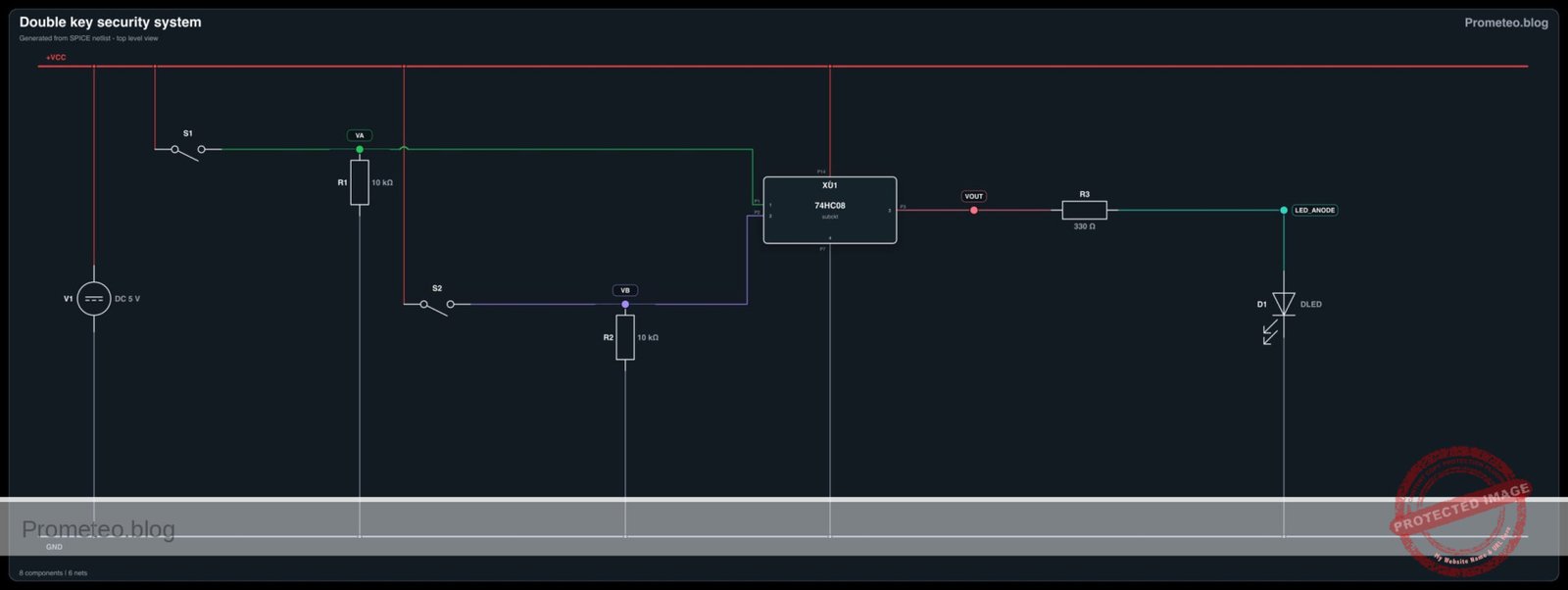
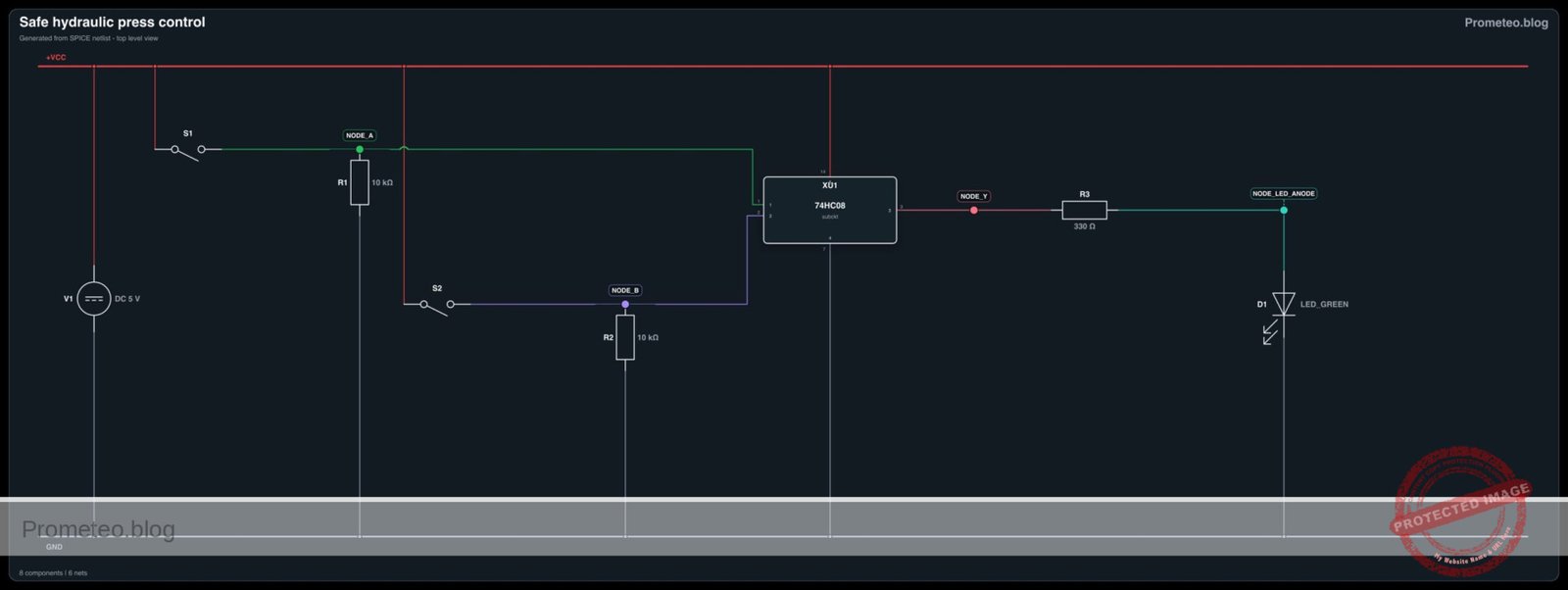
- U1: 74HC08, function: Quad 2-input AND gate IC.
- V1: 5 V DC supply, function: Main power source.
- SW1: Normally Open (NO) Pushbutton, function: Left-hand safety trigger.
- SW2: Normally Open (NO) Pushbutton, function: Right-hand safety trigger.
- R1: 10 kΩ resistor, function: Pull-down resistor for Input A.
- R2: 10 kΩ resistor, function: Pull-down resistor for Input B.
- R3: 330 Ω resistor, function: Current limiting for output LED.
- D1: Green LED, function: Indicator for «Motor Active» (Load).
Pin-out of the 74HC08
The 74HC08 contains four independent AND gates. We will use the first gate.
| Pin | Name | Logic function | Connection in this case |
|---|---|---|---|
| 1 | 1A | Input A | Connected to Node A (SW1) |
| 2 | 1B | Input B | Connected to Node B (SW2) |
| 3 | 1Y | Output | Connected to Node Y (to LED driver) |
| 7 | GND | Ground | Connected to Node 0 |
| 14 | VCC | Supply Voltage | Connected to Node VCC (+5V) |
Wiring guide
Construct the circuit using the following node connections. Ensure the power supply is off while wiring.
-
Power Nodes:
- Connect V1 positive terminal to Node VCC.
- Connect V1 negative terminal to Node 0 (GND).
- Connect U1 Pin 14 to VCC.
- Connect U1 Pin 7 to 0.
-
Input A Logic (Left Hand):
- Connect one side of SW1 to VCC.
- Connect the other side of SW1 to Node A.
- Connect R1 between Node A and Node 0 (Pull-down).
- Connect U1 Pin 1 to Node A.
-
Input B Logic (Right Hand):
- Connect one side of SW2 to VCC.
- Connect the other side of SW2 to Node B.
- Connect R2 between Node B and Node 0 (Pull-down).
- Connect U1 Pin 2 to Node B.
-
Output Logic (Load):
- Connect U1 Pin 3 to Node Y.
- Connect R3 between Node Y and Node LED_ANODE.
- Connect D1 Anode to Node LED_ANODE.
- Connect D1 Cathode to Node 0.
Conceptual block diagram
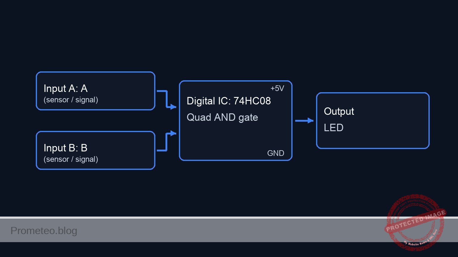
Schematic
Practical case: Safe Hydraulic Press Control

      [ INPUTS / SENSORS ]                  [ LOGIC PROCESSING ]                  [ OUTPUT / ACTUATOR ]

                                            +------------------+
(VCC) --> [ SW1: Left Hand ] --(Node A)---> |      Pin 1       |
               (NO Push)          |         |                  |
                                  v         |    U1: 74HC08    |
                              [ R1: 10k ]   |    (AND Gate)    |
                              (Pull-Down)   |                  | --(Node Y)--> [ R3: 330 ] --> [ D1: Green LED ] --> (GND)
                                  |         |      Pin 3       |               (Limit)         (Motor Active)
                                (GND)       |                  |
                                            |                  |
(VCC) --> [ SW2: Right Hand ]--(Node B)---> |      Pin 2       |
               (NO Push)          |         +------------------+
                                  v
                              [ R2: 10k ]
                              (Pull-Down)
                                  |
                                (GND)

Note: U1 Power Connections (Pin 14 to VCC, Pin 7 to GND) are implied for IC operation.
Electrical diagram
Truth table
This circuit implements the Boolean function $Y = A \cdot B$.
| SW1 (Input A) | SW2 (Input B) | Output Y (Logic) | LED Status | System State |
|---|---|---|---|---|
| Open (0) | Open (0) | Low (0) | OFF | Safe / Stop |
| Open (0) | Closed (1) | Low (0) | OFF | Safe / Stop |
| Closed (1) | Open (0) | Low (0) | OFF | Safe / Stop |
| Closed (1) | Closed (1) | High (1) | ON | Active / Run |
Measurements and tests
- Preparation: Set your multimeter to DC Voltage mode. Power on the V1 source (5 V).
- Idle Check: With no buttons pressed, measure the voltage at Node Y. It should be $\approx$ 0 V. The LED is OFF.
- Single Button Test: Press and hold SW1 only. Measure voltage at Node A ($\approx$ 5 V) and Node Y ($\approx$ 0 V). The LED remains OFF.
- Single Button Test: Press and hold SW2 only. Measure voltage at Node B ($\approx$ 5 V) and Node Y ($\approx$ 0 V). The LED remains OFF.
- Simultaneous Activation: Press both SW1 and SW2. Measure voltage at Node Y. It should read $\approx$ 3.5 V to 4.5 V (depending on the specific HC/LS logic family load and VCC). The LED turns ON.
SPICE netlist and simulation
Reference SPICE Netlist (ngspice) — excerptFull SPICE netlist (ngspice)
* Practical case: Safe Hydraulic Press Control

.title Safe Hydraulic Press Control

*******************************************************************************
* Component Models
*******************************************************************************

* Pushbutton Switch Model (Ideal Voltage Controlled Switch)
* Simulates the mechanical contact closing when control voltage is high (> 2.5V)
.model SW_PUSH SW(Vt=2.5 Vh=0.1 Ron=0.01 Roff=10Meg)

* LED Model (Green)
* Standard Green LED parameters
.model LED_GREEN D(IS=1e-22 RS=10 N=2 BV=5 IBV=10u CJO=10p TT=10n)

* 74HC08 Quad 2-input AND Gate (Behavioral Model for Simulation)
* Implements one gate of the IC.
* Pins: 1=InputA, 2=InputB, 3=OutputY, 7=GND, 14=VCC
.subckt 74HC08_GATE 1 2 3 7 14
    * Behavioral Voltage Source using continuous Sigmoid function for convergence
    * Y = VCC * (Sigmoid(A) * Sigmoid(B))
    * Threshold centered at 2.5V with steep slope (k=50)
    B1 3 7 V = V(14) * (1 / (1 + exp(-50 * (V(1) - 2.5)))) * (1 / (1 + exp(-50 * (V(2) - 2.5))))
.ends

*******************************************************************************
* Main Power Supply
*******************************************************************************
* V1: 5V DC supply connected to Node VCC and Node 0 (GND)
* ... (truncated in public view) ...
Copy this content into a .cir file and run with ngspice.
* Practical case: Safe Hydraulic Press Control

.title Safe Hydraulic Press Control

*******************************************************************************
* Component Models
*******************************************************************************

* Pushbutton Switch Model (Ideal Voltage Controlled Switch)
* Simulates the mechanical contact closing when control voltage is high (> 2.5V)
.model SW_PUSH SW(Vt=2.5 Vh=0.1 Ron=0.01 Roff=10Meg)

* LED Model (Green)
* Standard Green LED parameters
.model LED_GREEN D(IS=1e-22 RS=10 N=2 BV=5 IBV=10u CJO=10p TT=10n)

* 74HC08 Quad 2-input AND Gate (Behavioral Model for Simulation)
* Implements one gate of the IC.
* Pins: 1=InputA, 2=InputB, 3=OutputY, 7=GND, 14=VCC
.subckt 74HC08_GATE 1 2 3 7 14
    * Behavioral Voltage Source using continuous Sigmoid function for convergence
    * Y = VCC * (Sigmoid(A) * Sigmoid(B))
    * Threshold centered at 2.5V with steep slope (k=50)
    B1 3 7 V = V(14) * (1 / (1 + exp(-50 * (V(1) - 2.5)))) * (1 / (1 + exp(-50 * (V(2) - 2.5))))
.ends

*******************************************************************************
* Main Power Supply
*******************************************************************************
* V1: 5V DC supply connected to Node VCC and Node 0 (GND)
V1 VCC 0 DC 5

*******************************************************************************
* Input A Logic (Left Hand)
*******************************************************************************
* V_ACT_LEFT: Virtual actuator (Finger) for Left Button
* Generates a pulse: ON for 50us, OFF for 50us (Period 100us)
V_ACT_LEFT CTRL_LEFT 0 PULSE(0 5 0 1u 1u 50u 100u)

* SW1: Left Safety Trigger
* Connects VCC to Node_A when CTRL_LEFT is High
S1 VCC Node_A CTRL_LEFT 0 SW_PUSH

* R1: 10k Pull-down resistor for Input A
R1 Node_A 0 10k

*******************************************************************************
* Input B Logic (Right Hand)
*******************************************************************************
* V_ACT_RIGHT: Virtual actuator (Finger) for Right Button
* Generates a pulse: ON for 100us, OFF for 100us (Period 200us)
* Timing creates overlap with Left button to test AND logic (1+1, 0+1, 1+0, 0+0)
V_ACT_RIGHT CTRL_RIGHT 0 PULSE(0 5 0 1u 1u 100u 200u)

* SW2: Right Safety Trigger
* Connects VCC to Node_B when CTRL_RIGHT is High
S2 VCC Node_B CTRL_RIGHT 0 SW_PUSH

* R2: 10k Pull-down resistor for Input B
R2 Node_B 0 10k

*******************************************************************************
* Logic Processing (U1: 74HC08)
*******************************************************************************
* U1: AND Gate processing Left (A) and Right (B) inputs
* Connections: Pin1=Node_A, Pin2=Node_B, Pin3=Node_Y, Pin7=0(GND), Pin14=VCC
XU1 Node_A Node_B Node_Y 0 VCC 74HC08_GATE

*******************************************************************************
* Output Logic (Load)
*******************************************************************************
* R3: Current limiting resistor (330 Ohm)
R3 Node_Y Node_LED_ANODE 330

* D1: Green LED Indicator (Motor Active)
* Anode to R3, Cathode to GND
D1 Node_LED_ANODE 0 LED_GREEN

*******************************************************************************
* Simulation Commands
*******************************************************************************
* Transient analysis for 250us to cover full truth table sequence
.tran 1u 250u

* Print directives for logging signal states
.print tran V(Node_A) V(Node_B) V(Node_Y) V(Node_LED_ANODE)

.end
Simulation Results (Transient Analysis)

Show raw data table (786 rows)
Index   time            v(node_a)       v(node_b)       v(node_y)
0	0.000000e+00	4.995005e-03	4.995005e-03	2.199277e-108
1	1.000000e-08	4.995005e-03	4.995005e-03	2.199277e-108
2	2.000000e-08	4.995005e-03	4.995005e-03	2.199277e-108
3	4.000000e-08	4.995005e-03	4.995005e-03	2.199277e-108
4	8.000000e-08	4.995005e-03	4.995005e-03	2.199277e-108
5	1.600000e-07	4.995005e-03	4.995005e-03	2.199277e-108
6	3.200000e-07	4.995005e-03	4.995005e-03	2.199277e-108
7	3.600000e-07	4.995005e-03	4.995005e-03	2.199277e-108
8	4.300000e-07	4.995005e-03	4.995005e-03	2.199277e-108
9	4.493750e-07	4.995005e-03	4.995005e-03	2.199277e-108
10	4.832812e-07	4.995005e-03	4.995005e-03	2.199277e-108
11	5.162979e-07	4.999995e+00	4.999995e+00	5.000000e+00
12	5.474468e-07	4.999995e+00	4.999995e+00	5.000000e+00
13	5.779894e-07	4.999995e+00	4.999995e+00	5.000000e+00
14	6.039341e-07	4.999995e+00	4.999995e+00	5.000000e+00
15	6.320124e-07	4.999995e+00	4.999995e+00	5.000000e+00
16	6.881690e-07	4.999995e+00	4.999995e+00	5.000000e+00
17	8.004820e-07	4.999995e+00	4.999995e+00	5.000000e+00
18	1.000000e-06	4.999995e+00	4.999995e+00	5.000000e+00
19	1.022463e-06	4.999995e+00	4.999995e+00	5.000000e+00
20	1.067388e-06	4.999995e+00	4.999995e+00	5.000000e+00
21	1.157238e-06	4.999995e+00	4.999995e+00	5.000000e+00
22	1.336939e-06	4.999995e+00	4.999995e+00	5.000000e+00
23	1.696341e-06	4.999995e+00	4.999995e+00	5.000000e+00
... (762 more rows) ...
Common mistakes and how to avoid them
- Floating Inputs: Forgetting R1 or R2 causes the inputs to «float» when buttons are open, leading to erratic LED flickering or false triggering. Solution: Ensure pull-down resistors connect the inputs to ground.
- Confusing 7408 with 7400: The 7408 is an AND gate; the 7400 is a NAND gate. If the LED is ON when buttons are not pressed, you likely used the wrong chip. Solution: Check the markings on the IC package.
- LED Polarity: The LED does not light up even when Logic Y is High. Solution: Ensure the longer leg (Anode) faces the resistor/IC and the shorter leg (Cathode) faces Ground.
Troubleshooting
- Symptom: LED is always ON, regardless of buttons.
- Cause: Input pins shorted to VCC or incorrect IC (e.g., OR gate 74HC32 used by mistake).
- Fix: Check wiring at Pins 1 and 2; verify IC part number.
- Symptom: LED is very dim when both buttons are pressed.
- Cause: R3 value is too high or VCC is too low.
- Fix: Ensure R3 is around 220 Ω to 330 Ω; check V1 is 5 V.
- Symptom: Circuit works for one button but ignores the other.
- Cause: Broken switch or disconnected jumper wire on one input.
- Fix: Use a multimeter to verify continuity across SW1 and SW2 when pressed.
Possible improvements and extensions
- Power Interface: Replace the LED with an NPN transistor (like 2N2222) and a relay to control a real high-voltage motor.
- Master Enable Switch: Add a third switch connected to a third input (using a 3-input AND gate like 74HC11) to act as a «Key Switch» that must be active before the two hand buttons work.
More Practical Cases on Prometeo.blog
Find this product and/or books on this topic on Amazon
As an Amazon Associate, I earn from qualifying purchases. If you buy through this link, you help keep this project running.
Quick Quiz

Telecommunications Electronics Engineer and Computer Engineer (official degrees in Spain).