Level: Medium. Implement an XOR logic function using universal NAND gates to control a light source from two independent locations.
Objective and use case
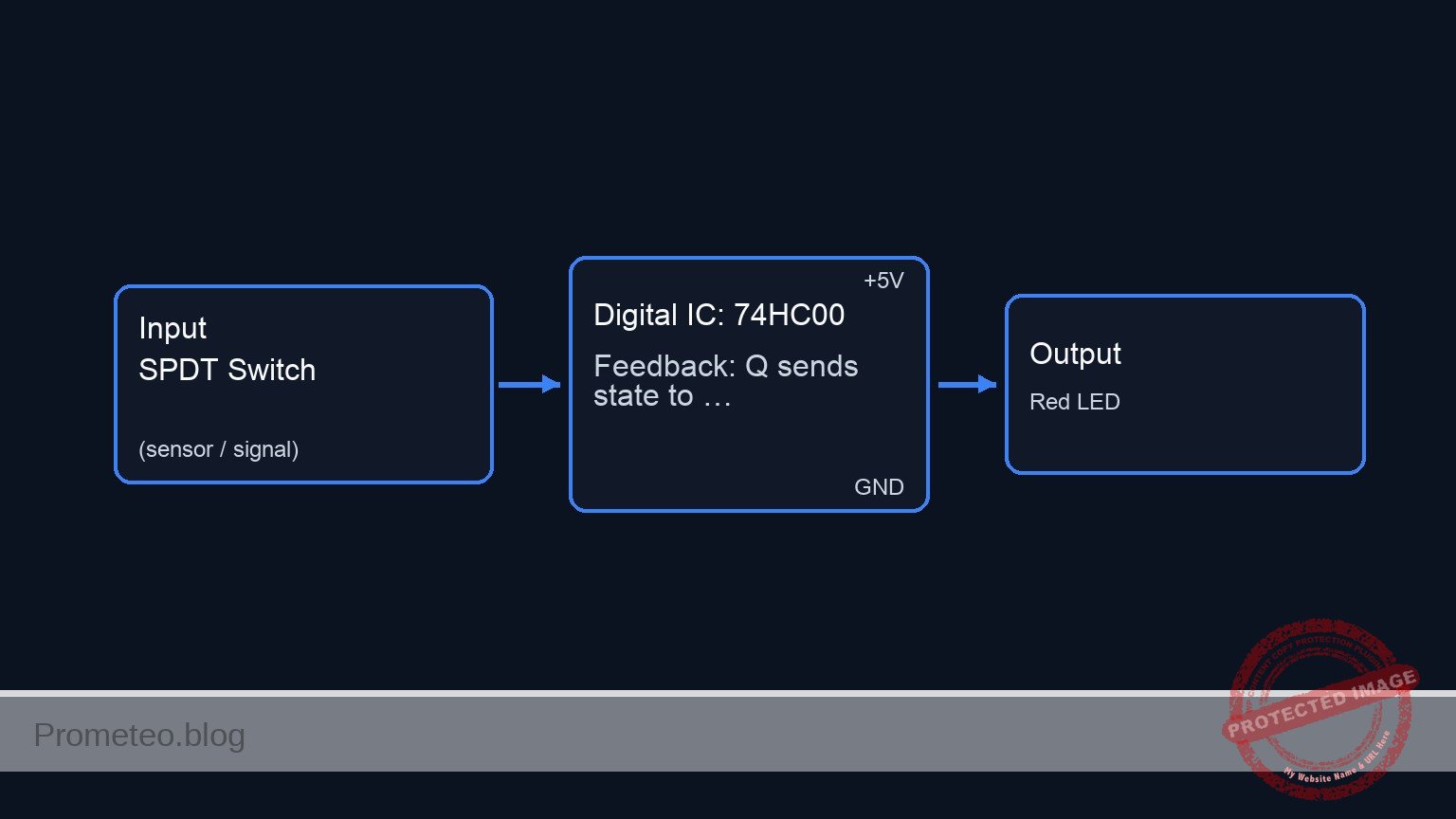
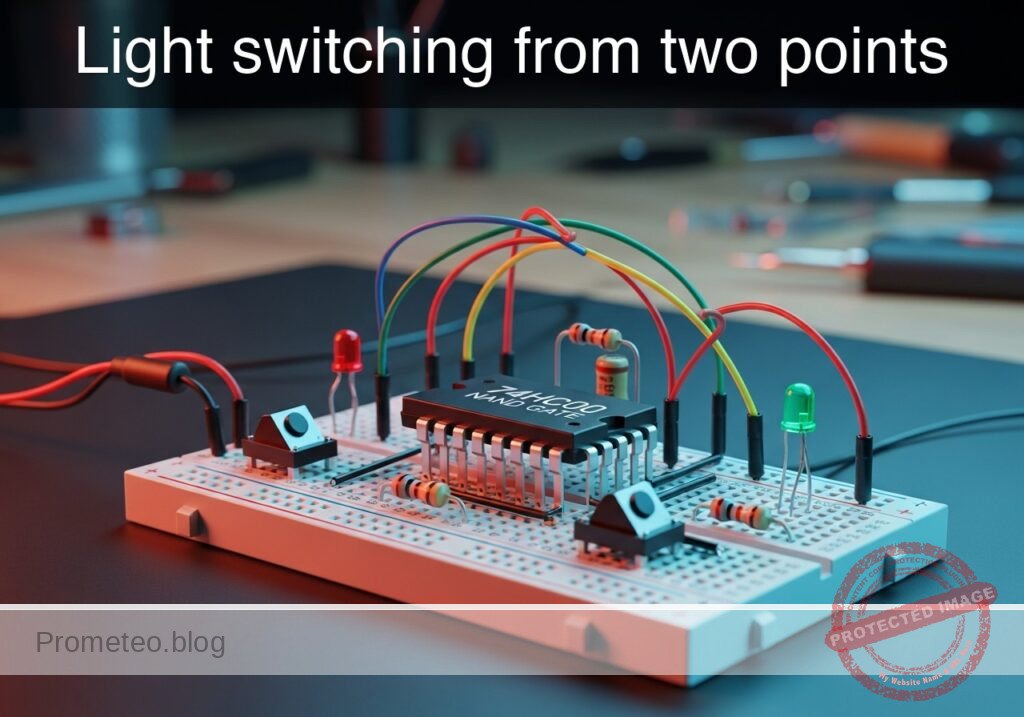
In this case, you will build a digital logic circuit that replicates a residential 2-way switching system (hallway light) using a single 74HC00 Quad NAND Gate IC. By combining four NAND gates, you will synthesize the Exclusive-OR (XOR) function, proving that NAND gates are «universal» building blocks.
Why it is useful:
* Residential wiring simulation: Demonstrates how two switches can independently toggle a single load (hallway/staircase logic).
* Digital Logic Synthesis: Teaches how to build complex logic (XOR) from basic universal gates (NAND).
* Arithmetic Circuits: This specific XOR topology is the fundamental component of a digital «Half-Adder» used in CPU ALUs.
* Error Detection: XOR logic is used to calculate parity bits for data transmission.
Expected outcome:
* State 00: When both switches are OFF, the LED is OFF.
* State 01/10: When only one switch is ON, the LED is ON (High logic level > 3.5 V).
* State 11: When both switches are ON, the LED is OFF.
* Universality: Successful demonstration that 4 NAND gates = 1 XOR gate.
Target audience: Electronics students and hobbyists familiar with basic logic gates.
Materials
- V1: 5 V DC power supply, function: Main circuit power.
- U1: 74HC00, function: Quad 2-input NAND gate IC.
- S1: SPST Switch, function: Input A (Switch 1).
- S2: SPST Switch, function: Input B (Switch 2).
- R1: 10 kΩ resistor, function: Pull-down for Input A.
- R2: 10 kΩ resistor, function: Pull-down for Input B.
- R3: 330 Ω resistor, function: LED current limiting.
- D1: Red LED, function: Output indicator (Light).
Pin-out of the IC used
Selected Chip: 74HC00 (Quad 2-Input NAND Gate)
| Pin | Name | Logic Function | Connection in this case |
|---|---|---|---|
| 1 | 1 A | Input Gate 1 | Connect to Node INPUT_A |
| 2 | 1B | Input Gate 1 | Connect to Node INPUT_B |
| 3 | 1Y | Output Gate 1 | Internal Node NAND_1_OUT |
| 4 | 2 A | Input Gate 2 | Connect to Node INPUT_A |
| 5 | 2B | Input Gate 2 | Connect to Node NAND_1_OUT |
| 6 | 2Y | Output Gate 2 | Internal Node NAND_2_OUT |
| 7 | GND | Ground | Connect to Node 0 (GND) |
| 8 | 3Y | Output Gate 3 | Internal Node NAND_3_OUT |
| 9 | 3 A | Input Gate 3 | Connect to Node NAND_1_OUT |
| 10 | 3B | Input Gate 3 | Connect to Node INPUT_B |
| 11 | 4Y | Output Gate 4 | Connect to Node FINAL_OUT |
| 12 | 4 A | Input Gate 4 | Connect to Node NAND_2_OUT |
| 13 | 4B | Input Gate 4 | Connect to Node NAND_3_OUT |
| 14 | VCC | Power Supply | Connect to Node VCC (+5 V) |
Wiring guide
- V1: Connect positive terminal to node
VCCand negative terminal to node0. - U1 (Power): Connect Pin 14 to
VCCand Pin 7 to0. - S1: Connect one side to
VCCand the other to nodeINPUT_A. - R1: Connect between node
INPUT_Aand node0. - S2: Connect one side to
VCCand the other to nodeINPUT_B. - R2: Connect between node
INPUT_Band node0. - U1 (Gate 1): Connect Pin 1 to
INPUT_A, Pin 2 toINPUT_B. Pin 3 is nodeNAND_1_OUT. - U1 (Gate 2): Connect Pin 4 to
INPUT_A, Pin 5 toNAND_1_OUT. Pin 6 is nodeNAND_2_OUT. - U1 (Gate 3): Connect Pin 10 to
INPUT_B, Pin 9 toNAND_1_OUT. Pin 8 is nodeNAND_3_OUT. - U1 (Gate 4): Connect Pin 12 to
NAND_2_OUT, Pin 13 toNAND_3_OUT. Pin 11 is nodeFINAL_OUT. - R3: Connect between node
FINAL_OUTand the Anode of D1. - D1: Connect the Cathode to node
0.
Conceptual block diagram
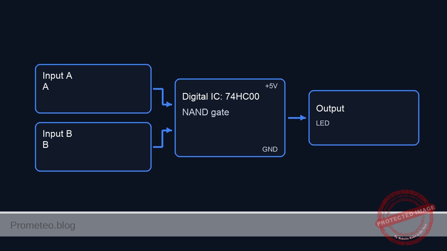
Schematic
Title: Practical case: Light switching from two points (XOR Logic)

INPUT STAGE                  LOGIC PROCESSING (74HC00)                  OUTPUT STAGE
(User Controls)              (NAND-based XOR Circuit)                   (Indicator)

                                     (Pin 4)
VCC --> [ S1 ] --(Node A)----------> [ U1:Gate 2 ] --(NAND_2)--\
          |                          (Pin 5,6)                  \
       [ R1 ]                            ^                       \
          v                              |                        \
         GND                        (NAND_1_OUT)                   \
                                         |                          \
                                         |                           \
(Node A) & (Node B) -----------> [ U1:Gate 1 ]                        --> [ U1:Gate 4 ] --(FINAL)--> [ R3 ] --> [ D1: LED ] --> GND
                                 (Pin 1,2->3)                        /    (Pin 12,13->11)
                                         |                          /
                                         |                         /
                                    (NAND_1_OUT)                  /
          ^                              |                       /
       [ R2 ]                            v                      /
          |                          (Pin 9)                   /
VCC --> [ S2 ] --(Node B)----------> [ U1:Gate 3 ] --(NAND_3)-/
                                     (Pin 10,8)
Truth table (Synthesized XOR)
| Switch A (S1) | Switch B (S2) | LED State (D1) | Logic Function |
|---|---|---|---|
| 0 (OFF) | 0 (OFF) | OFF (0) | No active input |
| 0 (OFF) | 1 (ON) | ON (1) | Inputs differ |
| 1 (ON) | 0 (OFF) | ON (1) | Inputs differ |
| 1 (ON) | 1 (ON) | OFF (0) | Inputs match |
Measurements and tests
- Initial State Check: Ensure both S1 and S2 are open. Measure voltage at Pin 11 (
FINAL_OUT). It should be < 0.5 V (Logic 0). D1 should be dark. - First Switch Toggle: Close S1 only. Measure voltage at Pin 11. It should be close to 5 V (Logic 1). D1 should light up.
- Second Switch Toggle: Open S1 and close S2. Observe D1. It should light up again (Logic 1).
- Collision Check: Close both S1 and S2 simultaneously. Measure voltage at Pin 3 (
NAND_1_OUT). Since both inputs are High, Pin 3 must be Low. Consequently, Pin 11 (FINAL_OUT) should go Low, turning D1 OFF.
SPICE netlist and simulation
Reference SPICE Netlist (ngspice) — excerptFull SPICE netlist (ngspice)
* Practical case: Light switching from two points
* Title: Light switching from two points

* ==============================================================================
* COMPONENT MODELS
* ==============================================================================

* Simple LED Model
.model DLED D(IS=1e-22 RS=10 N=1.5 CJO=10p BV=5 IBV=10u)

* Voltage Controlled Switch Model for Buttons
* Vt=2.5V threshold, Ron=1 ohm, Roff=10Meg ohm
.model SW_PUSH SW(Vt=2.5 Ron=1 Roff=10Meg)

* ==============================================================================
* MAIN CIRCUIT
* ==============================================================================

* --- Power Supply ---
* V1: 5 V DC power supply
* ... (truncated in public view) ...
Copy this content into a .cir file and run with ngspice.
* Practical case: Light switching from two points
* Title: Light switching from two points

* ==============================================================================
* COMPONENT MODELS
* ==============================================================================

* Simple LED Model
.model DLED D(IS=1e-22 RS=10 N=1.5 CJO=10p BV=5 IBV=10u)

* Voltage Controlled Switch Model for Buttons
* Vt=2.5V threshold, Ron=1 ohm, Roff=10Meg ohm
.model SW_PUSH SW(Vt=2.5 Ron=1 Roff=10Meg)

* ==============================================================================
* MAIN CIRCUIT
* ==============================================================================

* --- Power Supply ---
* V1: 5 V DC power supply
V1 VCC 0 DC 5

* --- Input A (Switch 1) ---
* Simulating physical switch S1 connecting VCC to INPUT_A
* Controlled by V_ACT_S1 (User pressing the button)
* Timing: Period 100us, Width 50us (Toggles faster)
V_ACT_S1 S1_CTRL 0 PULSE(0 5 0 1u 1u 50u 100u)
S1 VCC INPUT_A S1_CTRL 0 SW_PUSH

* R1: 10 kΩ pull-down for Input A
R1 INPUT_A 0 10k

* --- Input B (Switch 2) ---
* Simulating physical switch S2 connecting VCC to INPUT_B
* Controlled by V_ACT_S2 (User pressing the button)
* Timing: Period 200us, Width 100us (Toggles slower)
V_ACT_S2 S2_CTRL 0 PULSE(0 5 0 1u 1u 100u 200u)
S2 VCC INPUT_B S2_CTRL 0 SW_PUSH

* R2: 10 kΩ pull-down for Input B
R2 INPUT_B 0 10k

* --- Logic IC U1: 74HC00 ---
* Quad 2-input NAND gate IC
* Pin connections per Wiring Guide:
* P1=INPUT_A, P2=INPUT_B, P3=NAND_1_OUT
* P4=INPUT_A, P5=NAND_1_OUT, P6=NAND_2_OUT
* P7=0 (GND)
* P8=NAND_3_OUT, P9=NAND_1_OUT, P10=INPUT_B
* P11=FINAL_OUT, P12=NAND_2_OUT, P13=NAND_3_OUT
* P14=VCC
XU1 INPUT_A INPUT_B NAND_1_OUT INPUT_A NAND_1_OUT NAND_2_OUT 0 NAND_3_OUT NAND_1_OUT INPUT_B FINAL_OUT NAND_2_OUT NAND_3_OUT VCC 74HC00

* --- Output Stage ---
* R3: 330 Ω resistor
R3 FINAL_OUT LED_NODE 330

* D1: Red LED
D1 LED_NODE 0 DLED

* ==============================================================================
* SUBCIRCUITS
* ==============================================================================

* Subcircuit for 74HC00 Quad 2-Input NAND Gate
* Uses continuous behavioral sources for robust convergence
* Pinout: 1=1A, 2=1B, 3=1Y, 4=2A, 5=2B, 6=2Y, 7=GND, 8=3Y, 9=3A, 10=3B, 11=4Y, 12=4A, 13=4B, 14=VCC
.subckt 74HC00 1 2 3 4 5 6 7 8 9 10 11 12 13 14
    * Gate 1 (1,2 -> 3)
    * Logic: Vout = VCC * (1 - (High(A) * High(B)))
    Bg1 3 7 V={V(14,7)*(1-(1/(1+exp(-50*(V(1,7)-2.5))))*(1/(1+exp(-50*(V(2,7)-2.5)))))}

    * Gate 2 (4,5 -> 6)
    Bg2 6 7 V={V(14,7)*(1-(1/(1+exp(-50*(V(4,7)-2.5))))*(1/(1+exp(-50*(V(5,7)-2.5)))))}

    * Gate 3 (9,10 -> 8)
    Bg3 8 7 V={V(14,7)*(1-(1/(1+exp(-50*(V(9,7)-2.5))))*(1/(1+exp(-50*(V(10,7)-2.5)))))}

    * Gate 4 (12,13 -> 11)
    Bg4 11 7 V={V(14,7)*(1-(1/(1+exp(-50*(V(12,7)-2.5))))*(1/(1+exp(-50*(V(13,7)-2.5)))))}
.ends

* ==============================================================================
* ANALYSIS COMMANDS
* ==============================================================================

.op
.tran 1u 500u

* Print critical nodes including Inputs and the Output driving the LED
.print tran V(INPUT_A) V(INPUT_B) V(FINAL_OUT) V(LED_NODE)

.end
* --- GPT review (BOM/Wiring/SPICE) ---
* circuit_ok=true
* simulation_summary: The simulation confirms the XOR logic behavior required for 2-way switching. When inputs differ (e.g., t=51us: A=0, B=1 -> Out=5V; t=101us: A=1, B=1 -> Out=0V; t=180us: A=1, B=0 -> Out=5V), the LED is ON (approx 1.88V drop). When inputs match (0,0 or 1,1), the output is near 0V.
* bom_vs_spice equivalences ignored:
*   - Physical switches S1 and S2 are modeled as voltage-controlled switches (SW_PUSH) driven by PULSE sources (V_ACT_S1, V_ACT_S2) to simulate user interaction.
*   - The 74HC00 Quad NAND IC is modeled as a behavioral subcircuit using mathematical expressions for logic gates.
*   - The LED D1 is modeled as a generic diode DLED with specific parameters.
* overall_comment: The circuit is a classic XOR implementation using four NAND gates, correctly wired to simulate a 2-way light switch (staircase switch). The SPICE netlist accurately represents the BOM and wiring guide. The simulation results perfectly match the provided truth table: the LED lights up only when the switch states are different.
* --------------------------------------
Simulation Results (Transient Analysis)

Show raw data table (773 rows)
Index   time            v(input_a)      v(input_b)      v(final_out)    v(led_node)
0	0.000000e+00	4.995005e-03	4.995005e-03	-3.70921e-68	-1.32951e-36
1	1.000000e-08	4.995005e-03	4.995005e-03	-3.70921e-68	-3.37339e-37
2	2.000000e-08	4.995005e-03	4.995005e-03	-3.70921e-68	1.661518e-37
3	4.000000e-08	4.995005e-03	4.995005e-03	-3.70921e-68	2.976605e-37
4	8.000000e-08	4.995005e-03	4.995005e-03	-3.70921e-68	8.146600e-38
5	1.600000e-07	4.995005e-03	4.995005e-03	-3.70921e-68	-2.74917e-38
6	3.200000e-07	4.995005e-03	4.995005e-03	-3.70921e-68	-1.00046e-38
7	3.562500e-07	4.995005e-03	4.995005e-03	-3.70921e-68	-9.54478e-40
8	4.196875e-07	4.995005e-03	4.995005e-03	-3.70921e-68	1.440911e-39
9	4.372461e-07	4.995005e-03	4.995005e-03	-3.70921e-68	5.873353e-40
10	4.679736e-07	4.995005e-03	4.995005e-03	-3.70921e-68	-1.64244e-40
11	5.019934e-07	4.999500e+00	4.999500e+00	-3.70921e-68	5.471353e-16
12	5.700330e-07	4.999500e+00	4.999500e+00	-3.70921e-68	1.883035e-16
13	7.061121e-07	4.999500e+00	4.999500e+00	-3.70921e-68	-1.89304e-16
14	9.782703e-07	4.999500e+00	4.999500e+00	-3.70921e-68	1.713539e-16
15	1.000000e-06	4.999500e+00	4.999500e+00	-3.70921e-68	-8.76370e-17
16	1.043459e-06	4.999500e+00	4.999500e+00	-3.70921e-68	2.969253e-18
17	1.130378e-06	4.999500e+00	4.999500e+00	-3.70921e-68	1.336375e-17
18	1.304216e-06	4.999500e+00	4.999500e+00	-3.70921e-68	1.285658e-18
19	1.651892e-06	4.999500e+00	4.999500e+00	-3.70921e-68	-4.38731e-19
20	2.347244e-06	4.999500e+00	4.999500e+00	-3.70921e-68	-3.76487e-20
21	3.347244e-06	4.999500e+00	4.999500e+00	-3.70921e-68	3.641502e-21
22	4.347244e-06	4.999500e+00	4.999500e+00	-3.70921e-68	3.034717e-22
23	5.347244e-06	4.999500e+00	4.999500e+00	-3.70921e-68	-2.04956e-23
... (749 more rows) ...
Common mistakes and how to avoid them
- Floating Inputs: Forgetting R1 or R2 causes the inputs to «float,» often reading as High due to electromagnetic noise. Solution: Always ensure inputs are pulled to Ground when the switch is open.
- Incorrect Gate Feedback: Wiring Pin 3 output to the wrong inputs on Gates 2 or 3 destroys the logic. Solution: Double-check that the output of the first NAND (Pin 3) connects to BOTH the second (Pin 5) and third (Pin 9) gates.
- Forgetting Power: Logic chips do not work passively. Solution: Verify 5 V on Pin 14 and continuity to Ground on Pin 7 before inserting signals.
Troubleshooting
- Symptom: LED is always ON, regardless of switch position.
- Cause: Wiring error at the final NAND gate (Gate 4) or output shorted to VCC.
- Fix: Check connections at Pins 11, 12, and 13. Ensure Pin 11 is not touching the positive rail.
- Symptom: LED behaves like an OR gate (stays ON when both switches are ON).
- Cause: The first NAND gate (Gate 1) is not effectively inhibiting the signal.
- Fix: Check continuity on Pins 1, 2, and 3. If Gate 1 output stays High when inputs are High, the XOR logic fails.
- Symptom: Circuit works erratically when touching the wires.
- Cause: Missing pull-down resistors (floating inputs).
- Fix: Verify R1 and R2 are securely connected between the input pins and Ground.
Possible improvements and extensions
- 3-Way Switching: Add a third switch and another XOR stage (using a second 74HC00 or a 74HC86) to control the light from three locations.
- Comparison with Dedicated IC: Build the same circuit using a 74HC86 (Quad XOR) alongside this one to compare propagation delay and wiring complexity.
More Practical Cases on Prometeo.blog
Find this product and/or books on this topic on Amazon
As an Amazon Associate, I earn from qualifying purchases. If you buy through this link, you help keep this project running.
Quick Quiz

Telecommunications Electronics Engineer and Computer Engineer (official degrees in Spain).