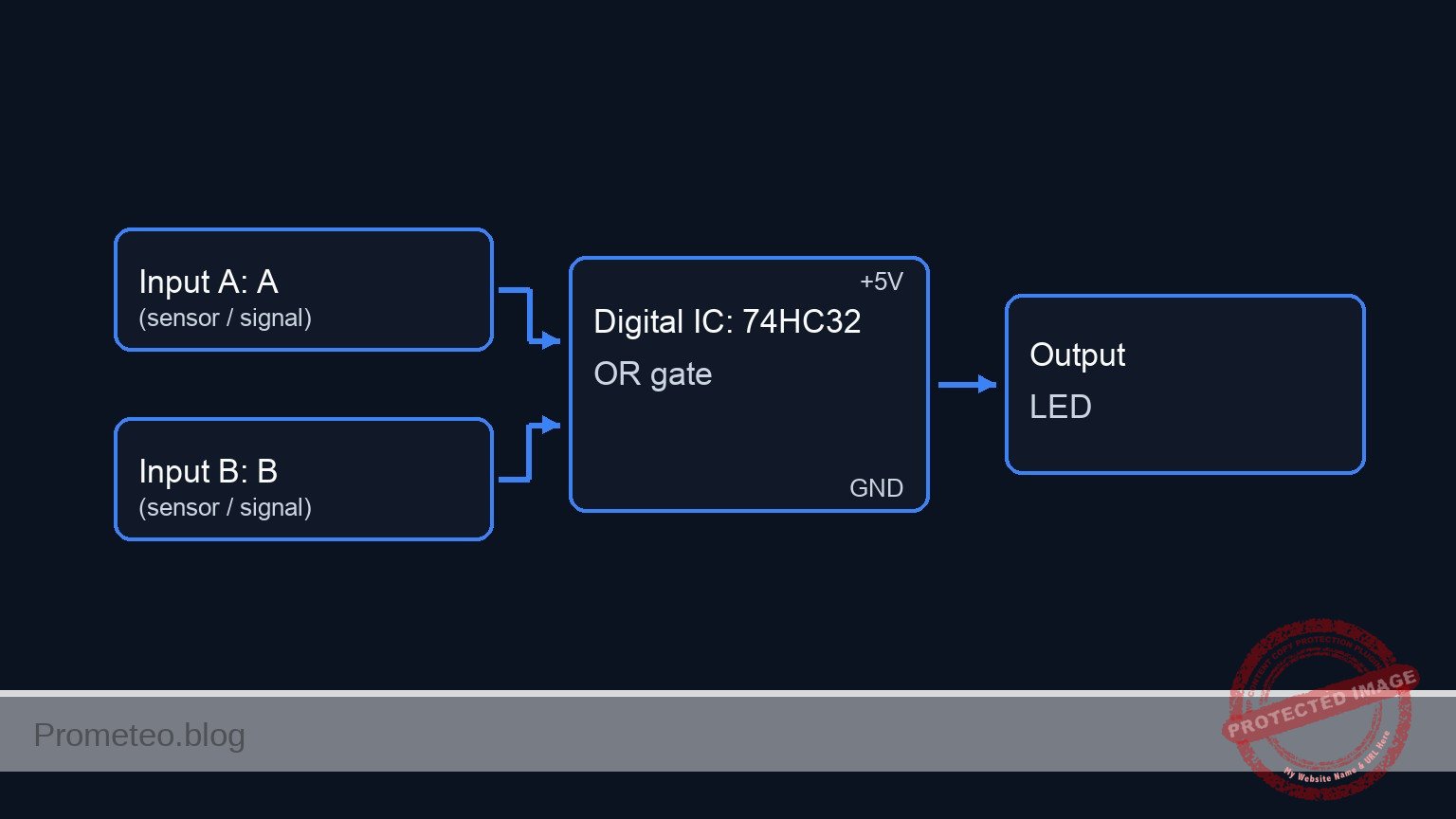
Level: Medium. Design a logic circuit that alerts the user when a water sensor stops detecting liquid using a NOT gate.
Objective and use case
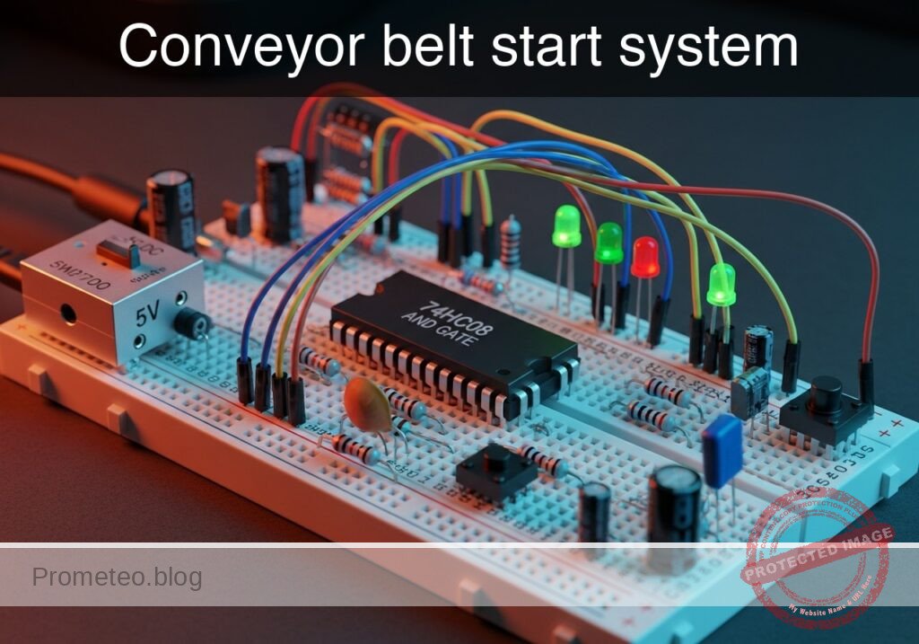
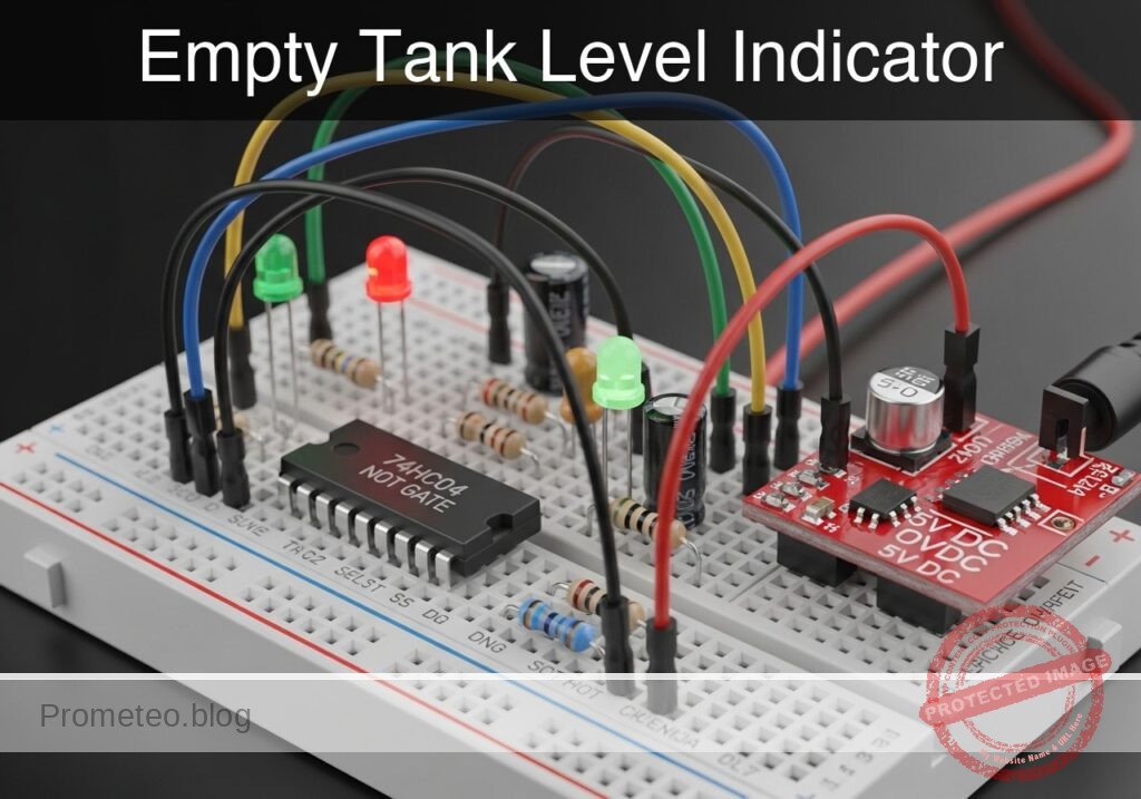
In this case, you will build a monitoring circuit using a 74HC04 inverter that illuminates a red LED when a tank’s liquid level drops below a critical point.
- Prevents pump damage: Stops water pumps from running dry in hydroponic systems.
- Household safety: Alerts when rooftop reserve tanks are empty.
- Industrial maintenance: Visual flag for coolant refill requirements.
Expected outcome:
* Water Present: The sensor is open (Logic 1 input) $\rightarrow$ LED remains OFF.
* Tank Empty: The sensor closes (Logic 0 input) $\rightarrow$ LED turns ON.
* Logic Level: $V_{in} \approx 0\text{ V}$ activates the alert; $V_{in} \approx 5\text{ V}$ indicates normal status.
Target audience: Electronics students and hobbyists familiar with basic digital logic.
Materials
- V1: 5 V DC power supply, function: main circuit power
- U1: 74HC04 Hex Inverter IC, function: logic inversion
- S1: Float switch (SPST, configured to Close when Empty), function: liquid level sensor
- R1: 10 kΩ resistor, function: pull-up for sensor signal
- R2: 330 Ω resistor, function: LED current limiting
- D1: Red LED, function: visual empty alert
- C1: 100 nF ceramic capacitor, function: power supply decoupling
Pin-out of the IC used
Selected Chip: 74HC04 (Hex Inverter)
| Pin | Name | Logic function | Connection in this case |
|---|---|---|---|
| 1 | 1A | Input | Connected to Sensor Node (SENSE_IN) |
| 2 | 1Y | Output | Connected to LED circuit (ALERT_OUT) |
| 7 | GND | Ground | Connected to GND (0 V) |
| 14 | VCC | Power | Connected to 5 V Supply |
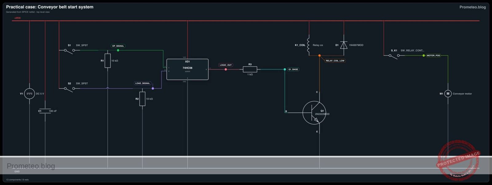
Wiring guide
- V1 connects between node
VCCand nodeGND. - C1 connects between node
VCCand nodeGND(placed physically close to U1). - R1 connects between node
VCCand nodeSENSE_IN. - S1 connects between node
SENSE_INand nodeGND. - U1 pin 1 connects to node
SENSE_IN. - U1 pin 2 connects to node
ALERT_OUT. - U1 pin 14 connects to
VCC; pin 7 connects toGND. - R2 connects between node
ALERT_OUTand nodeLED_ANODE. - D1 connects between node
LED_ANODE(Anode) and nodeGND(Cathode).
Conceptual block diagram
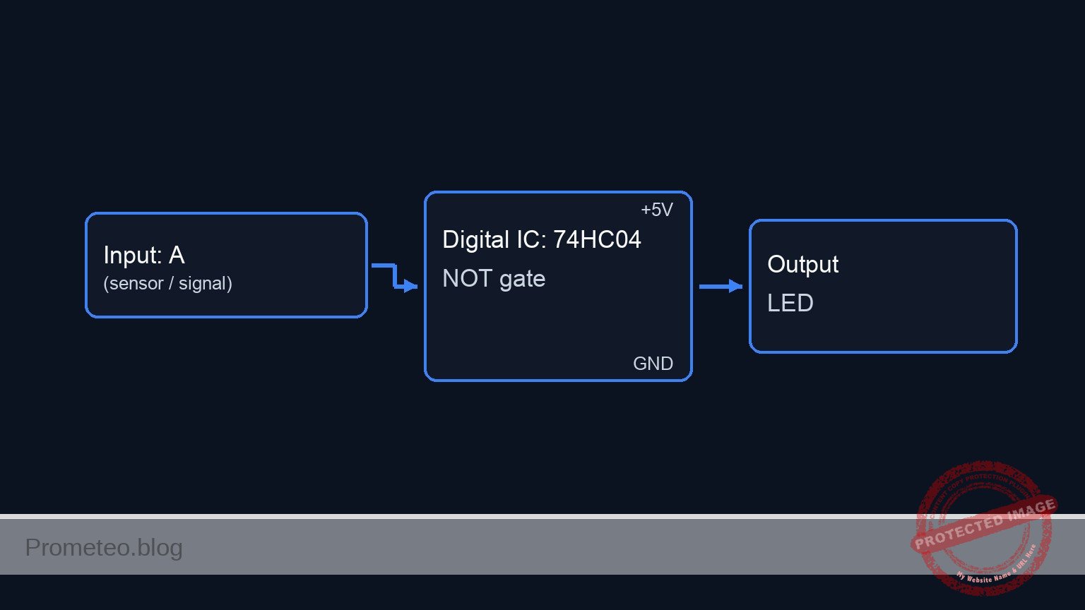
Schematic
[ INPUT / SENSOR ]                 [ LOGIC PROCESSING ]                 [ OUTPUT / ALERT ]

[ VCC 5V ] --> [ R1: 10k ] --+
               (Pull-Up)     |
                             |
                             V
                        (SENSE_IN) ---->+------------------+
                        (Pin 1)         |    U1: 74HC04    |
                             ^          |   Hex Inverter   |--(ALERT_OUT)--> [ R2: 330R ] --> [ D1: Red LED ] --> GND
                             |          |   (Pin 1 -> 2)   |  (Pin 2)        (Limiting)       (Anode/Cathode)
[ GND 0V ] --> [ S1: Float ]-+          +------------------+
               (Switch)                           ^
                                                  |
                                            [ C1: 100nF ]
                                            (Decoupling)
                                            (VCC / GND)
Truth table
| Water State | Sensor Switch (S1) | Input Voltage (Pin 1) | Logic Input | Output Voltage (Pin 2) | LED State |
|---|---|---|---|---|---|
| Full | OPEN | 5 V (via Pull-up) | 1 | 0 V | OFF |
| Empty | CLOSED | 0 V (connected to GND) | 0 | 5 V | ON |
Measurements and tests
- Supply Check: Measure voltage between
VCCandGND. Ensure it is stable at 5 V. - Full Tank Simulation: Manually lift the float (ensure S1 is OPEN). Measure voltage at
SENSE_IN. It should be $\approx 5\text{ V}$. Verify LED is OFF. - Empty Tank Simulation: Drop the float (ensure S1 is CLOSED). Measure voltage at
SENSE_IN. It should be $\approx 0\text{ V}$. - Logic Output: While S1 is closed (Empty), measure voltage at
ALERT_OUT. It should be $\approx 5\text{ V}$. - Current Draw: Measure the current through D1 ($I_{led}$) when ON. It should be approximately 10–12 mA depending on the specific LED voltage drop.
SPICE netlist and simulation
Reference SPICE Netlist (ngspice) — excerptFull SPICE netlist (ngspice)
* Practical case: Empty Tank Level Indicator

* ==============================================================================
* BILL OF MATERIALS & COMPONENTS
* ==============================================================================

* --- Power Supply ---
* V1: 5 V DC power supply
V1 VCC 0 DC 5

* --- Decoupling ---
* C1: 100 nF ceramic capacitor (Power supply decoupling)
C1 VCC 0 100n

* --- Sensor Input Section ---
* R1: 10 kΩ resistor (Pull-up for sensor signal)
R1 VCC SENSE_IN 10k

* S1: Float switch (SPST)
* Wiring: Connects between node SENSE_IN and node GND.
* ... (truncated in public view) ...
Copy this content into a .cir file and run with ngspice.
* Practical case: Empty Tank Level Indicator

* ==============================================================================
* BILL OF MATERIALS & COMPONENTS
* ==============================================================================

* --- Power Supply ---
* V1: 5 V DC power supply
V1 VCC 0 DC 5

* --- Decoupling ---
* C1: 100 nF ceramic capacitor (Power supply decoupling)
C1 VCC 0 100n

* --- Sensor Input Section ---
* R1: 10 kΩ resistor (Pull-up for sensor signal)
R1 VCC SENSE_IN 10k

* S1: Float switch (SPST)
* Wiring: Connects between node SENSE_IN and node GND.
* Simulation: Modeled as a Voltage Controlled Switch (SW).
* Logic:
*   - Tank Full (Float Up) -> Switch Open -> SENSE_IN pulled to VCC.
*   - Tank Empty (Float Down) -> Switch Closed -> SENSE_IN pulled to GND.
* Control Source V_FLOAT_ACT simulates the float movement.
*   - 0V = Float Up (Full)
*   - 5V = Float Down (Empty)
S1 SENSE_IN 0 FLOAT_CTRL 0 SW_FLOAT
.model SW_FLOAT SW(Vt=2.5 Ron=0.1 Roff=10Meg)

* Stimulus: Float starts Up (Full), drops to Down (Empty) at 50us, returns at 200us.
V_FLOAT_ACT FLOAT_CTRL 0 PULSE(0 5 50u 1u 1u 150u 400u)

* --- Logic Processing ---
* U1: 74HC04 Hex Inverter
* Wiring Guide: Pin 1 (In) -> SENSE_IN, Pin 2 (Out) -> ALERT_OUT
* Power: Pin 14 -> VCC, Pin 7 -> GND
* Implemented as a subcircuit to strictly map pins.
XU1 SENSE_IN ALERT_OUT 0 VCC 74HC04_GATE

* Subcircuit definition for one gate of 74HC04
.subckt 74HC04_GATE IN OUT GND VCC
    * Behavioral voltage source for robust logic inversion
    * Uses sigmoid function for convergence: Vout = VCC if Vin < 2.5V
    B1 OUT GND V = V(VCC) * (1 / (1 + exp(50 * (V(IN) - 2.5))))
.ends

* --- Output Alert ---
* R2: 330 Ω resistor (LED current limiting)
R2 ALERT_OUT LED_ANODE 330

* D1: Red LED (Visual empty alert)
* Wiring: Anode -> LED_ANODE, Cathode -> GND
D1 LED_ANODE 0 LED_RED
.model LED_RED D(IS=1e-14 N=2 RS=5 BV=5 IBV=10u CJO=40p)

* ==============================================================================
* ANALYSIS COMMANDS
* ==============================================================================

* Operating Point Analysis
.op

* Transient Analysis
* Run for 500us to capture the float switch activation cycle
.tran 1u 500u

* Output Printing
* Monitor Sensor Input, Inverter Output, and LED Voltage
.print tran V(SENSE_IN) V(ALERT_OUT) V(LED_ANODE) V(FLOAT_CTRL)

.end
Simulation Results (Transient Analysis)

Show raw data table (1190 rows)
Index   time            v(sense_in)     v(alert_out)    v(led_anode)
0	0.000000e+00	4.995005e+00	3.316079e-54	-1.70080e-28
1	1.000000e-08	4.995005e+00	3.316079e-54	-9.73961e-29
2	2.000000e-08	4.995005e+00	3.316079e-54	-1.41516e-29
3	4.000000e-08	4.995005e+00	3.316079e-54	8.723601e-29
4	8.000000e-08	4.995005e+00	3.316079e-54	1.163518e-28
5	1.600000e-07	4.995005e+00	3.316079e-54	4.380930e-29
6	3.200000e-07	4.995005e+00	3.316079e-54	-1.45299e-29
7	6.400000e-07	4.995005e+00	3.316079e-54	-1.01395e-29
8	1.280000e-06	4.995005e+00	3.316079e-54	-5.46095e-32
9	2.280000e-06	4.995005e+00	3.316079e-54	4.098577e-31
10	3.280000e-06	4.995005e+00	3.316079e-54	2.282032e-32
11	4.280000e-06	4.995005e+00	3.316079e-54	-9.50625e-33
12	5.280000e-06	4.995005e+00	3.316079e-54	-1.09186e-33
13	6.280000e-06	4.995005e+00	3.316079e-54	1.911218e-34
14	7.280000e-06	4.995005e+00	3.316079e-54	3.847480e-35
15	8.280000e-06	4.995005e+00	3.316079e-54	-2.97995e-36
16	9.280000e-06	4.995005e+00	3.316079e-54	-1.15977e-36
17	1.028000e-05	4.995005e+00	3.316079e-54	1.723722e-38
18	1.128000e-05	4.995005e+00	3.316079e-54	3.117034e-38
19	1.228000e-05	4.995005e+00	3.316079e-54	1.177223e-39
20	1.328000e-05	4.995005e+00	3.316079e-54	-7.52109e-40
21	1.428000e-05	4.995005e+00	3.316079e-54	-6.99870e-41
22	1.528000e-05	4.995005e+00	3.316079e-54	1.597704e-41
23	1.628000e-05	4.995005e+00	3.316079e-54	2.660714e-42
... (1166 more rows) ...
Common mistakes and how to avoid them
- Leaving inputs floating: Even though we only use one gate (Pin 1/2), unused inputs on CMOS chips (pins 3, 5, 9, 11, 13) should be tied to GND or VCC to prevent oscillation and excess power consumption.
- Incorrect Pull-up wiring: Connecting the resistor in series with the input instead of as a pull-up to VCC. Ensure R1 goes strictly to 5V.
- Sensor Logic inversion: Using a sensor that is Open when Empty without changing the circuit logic. This would cause the light to be ON when the tank is full. Ensure the mechanical action matches the truth table.
Troubleshooting
- LED is always ON: Check if S1 is stuck in the Closed position or if pin 1 is shorted to ground.
- LED never turns ON: Check if the float switch is actually closing the circuit to ground. Measure resistance across S1 terminals while moving the float.
- Chip gets hot: Check for short circuits at the output or if VCC/GND are reversed (Pins 14 and 7).
- LED flickers: The liquid might be turbulent. Add a capacitor (e.g., 10 µF) in parallel with S1 to create a hardware debounce delay.
Possible improvements and extensions
- Audio Alert: Add a 5V active buzzer in parallel with the LED/Resistor combo to provide an audible alarm when the tank is empty.
- Hysteresis: Replace the 74HC04 with a 74HC14 (Schmitt Trigger Inverter). This prevents the LED from jittering if the water level is right at the switching threshold.
More Practical Cases on Prometeo.blog
Quick Quiz

Telecommunications Electronics Engineer and Computer Engineer (official degrees in Spain).