Level: Medium | Construct a transistor-driven relay circuit to automatically control a water pump using a float switch.
Objective and use case
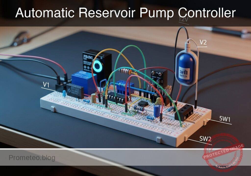
In this practical case, you will build an automatic reservoir pump controller. The circuit uses a mechanical float switch to trigger an NPN transistor, which energizes an electromechanical relay to drive a high-current DC pump (simulated here as a resistive load) and a status LED.
Why this is useful:
* Automates water level management in tanks, reservoirs, and sump basins.
* Safely isolates low-voltage control circuits from high-power loads.
* Demonstrates the practical interfacing of simple mechanical sensors with power electronics.
* Prevents overflow or dry-running conditions in industrial and agricultural settings.
Expected outcome:
* Closing the float switch applies a voltage to the transistor base, turning it on (saturation).
* The transistor sinks current for the relay coil, energizing it and closing its normally open (NO) contact.
* The simulated DC pump (load resistor) receives the full supply voltage.
* The status indicator LED illuminates when the pump is active.
* Releasing the switch de-energizes the relay, and the flyback diode safely dissipates the inductive voltage spike from the coil.
Target audience: Intermediate electronics students learning about transistor switching, electromechanical relays, and inductive load protection.
Materials
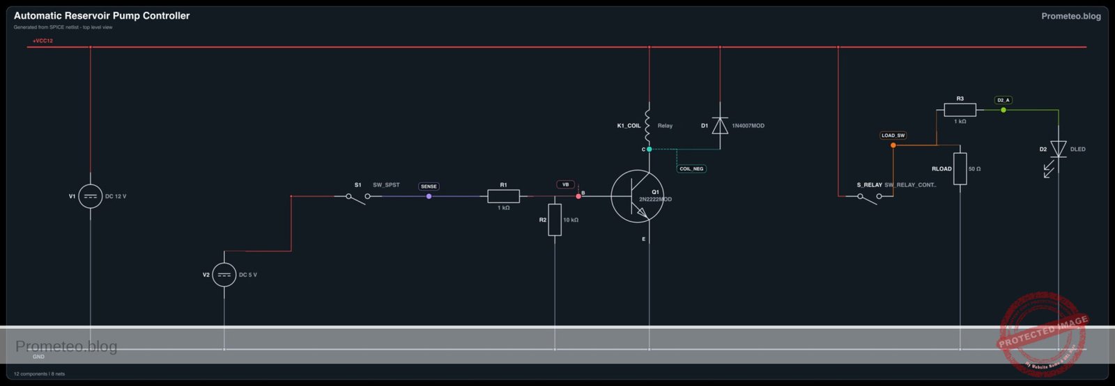
V1: 12 V DC supply, function: main power for relay coil and pumpV2: 5 V DC supply, function: control logic power for the float switchSW1: SPST switch, function: simulated float switch or high-level sensorR1: 1 kΩ resistor, function: transistor base current limitingR2: 10 kΩ resistor, function: pull-down for transistor base to ensure turn-offR3: 1 kΩ resistor, function: LED current limitingRLOAD: 50 Ω high-power resistor, function: simulated DC pump loadQ1: 2N2222 NPN transistor, function: relay coil driverD1: 1N4007 diode, function: flyback protection for relay coilD2: Green LED, function: pump status indicatorK1: 12 V SPDT Relay, function: electromechanical switch for the pump
Wiring guide
V1connects between nodeVCC12and node0.V2connects between nodeVCC5and node0.SW1connects between nodeVCC5and nodeSENSE.R1connects between nodeSENSEand nodeVB.R2connects between nodeVBand node0.Q1base connects to nodeVB, emitter connects to node0, and collector connects to nodeCOIL_NEG.K1coil connects between nodeVCC12and nodeCOIL_NEG.K1COM (Common) contact connects to nodeVCC12.K1NO (Normally Open) contact connects to nodeLOAD_SW.D1cathode connects to nodeVCC12and anode connects to nodeCOIL_NEG(placed anti-parallel to the relay coil).RLOADconnects between nodeLOAD_SWand node0.R3connects between nodeLOAD_SWand the anode ofD2.D2cathode connects to node0.
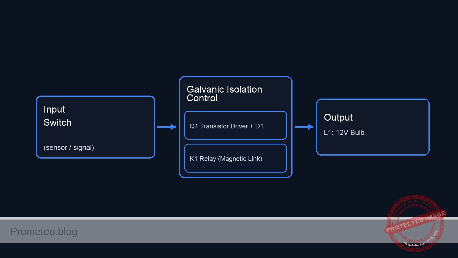
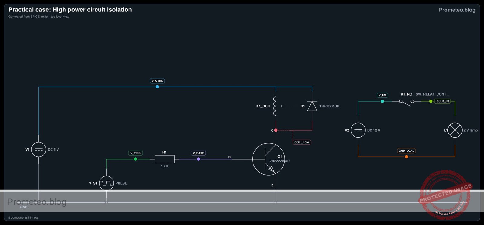
Conceptual block diagram
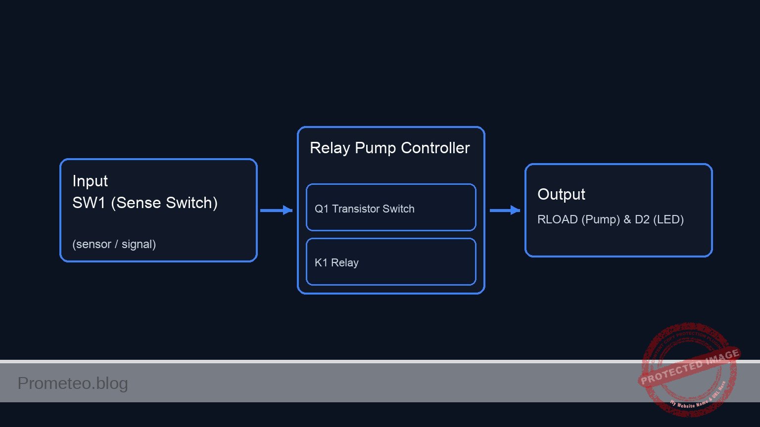
Schematic
VCC5 --> [ SW1 ] --(SENSE)--> [ R1 ] --(VB)--> [ Q1:B ]
                                              |          |
                                            [ R2 ]       |
                                              |          |
                                             GND         |
                                                         |
      VCC12 --> [ K1 Coil || D1(Rev) ] --(COIL_NEG)--> [ Q1:C ] --( )-- [ Q1:E ] --> GND
                       |
                (Magnetic Link)
                       v
      VCC12 --> [ K1 Switch (COM->NO) ] --(LOAD_SW)--> [ RLOAD (Pump) ] --> GND
                                              |
                                              +------> [ R3 ] --> [ D2 (LED) ] --> GND
Electrical diagram
Measurements and tests
- Control Logic Test: With
SW1open, measure the voltage at nodeSENSE. It should be 0 V. CloseSW1and verify the voltage rises to 5 V. - Base Drive Verification: Measure the voltage at node
VBwithSW1closed. It should read approximately 0.7 V, confirming the base-emitter junction ofQ1is forward-biased. - Coil Switching Verification: Probe node
COIL_NEG. WhenSW1is open, it should measure 12 V. WhenSW1is closed, it should drop to near 0 V (Vce_sat of the transistor), confirming the coil is energized. - Load Delivery Test: Measure the voltage at node
LOAD_SW. Verify that it reads 0 V when the relay is off, and jumps to 12 V when the relay clicks on. Check that theRLOADdraws current andD2illuminates.
SPICE netlist and simulation
Reference SPICE Netlist (ngspice) — excerptFull SPICE netlist (ngspice)
* Automatic Reservoir Pump Controller
.width out=256

* Power Supplies
V1 VCC12 0 DC 12
V2 VCC5 0 DC 5

* Simulated Float Switch (SW1)
* Using a voltage-controlled switch and a pulse source to simulate a user/sensor triggering the switch
V_SW_CTRL SW_CTRL 0 PULSE(0 5 50u 1u 1u 200u 500u)
S1 VCC5 SENSE SW_CTRL 0 myswitch

* Base driving circuit
R1 SENSE VB 1k
R2 VB 0 10k

* Relay Driver Transistor
Q1 COIL_NEG VB 0 2N2222MOD

* Relay Coil (K1)
* ... (truncated in public view) ...
Copy this content into a .cir file and run with ngspice.
* Automatic Reservoir Pump Controller
.width out=256

* Power Supplies
V1 VCC12 0 DC 12
V2 VCC5 0 DC 5

* Simulated Float Switch (SW1)
* Using a voltage-controlled switch and a pulse source to simulate a user/sensor triggering the switch
V_SW_CTRL SW_CTRL 0 PULSE(0 5 50u 1u 1u 200u 500u)
S1 VCC5 SENSE SW_CTRL 0 myswitch

* Base driving circuit
R1 SENSE VB 1k
R2 VB 0 10k

* Relay Driver Transistor
Q1 COIL_NEG VB 0 2N2222MOD

* Relay Coil (K1)
* Modeled as a series resistor and inductor
R_K1 VCC12 K1_COIL_INT 400
L_K1 K1_COIL_INT COIL_NEG 10mH

* Flyback Diode
D1 COIL_NEG VCC12 1N4007MOD

* Relay Contacts (K1 NO)
* The switch closes when the voltage across the coil (VCC12 - COIL_NEG) exceeds 8V
S_RELAY VCC12 LOAD_SW VCC12 COIL_NEG relay_sw

* Simulated Pump Load
RLOAD LOAD_SW 0 50

* Status LED
R3 LOAD_SW D2_A 1k
D2 D2_A 0 DLED

* Models
.model myswitch SW(vt=2.5 vh=0.5 ron=0.1 roff=10MEG)
.model relay_sw SW(vt=8 vh=1 ron=0.05 roff=100MEG)
.model 2N2222MOD NPN(IS=1E-14 VAF=100 BF=200 IKF=0.3 XTB=1.5 BR=3 CJC=8E-12 CJE=25E-12 TR=100E-9 TF=400E-12 ITF=1 VTF=2 XTF=3 RB=10)
.model 1N4007MOD D(IS=7.02767n RS=0.0341512 N=1.80803 EG=1.11 XTI=3.0 BV=1000 IBV=5e-08 CJO=1e-11 VJ=0.7 M=0.5 FC=0.5 TT=1e-07)
.model DLED D(IS=1e-20 N=2.2 RS=2.5 BV=5 IBV=10u CJO=50p)

* Analysis Commands
.op
.tran 1u 500u
.print tran V(SENSE) V(LOAD_SW) V(COIL_NEG) V(VB) I(L_K1)

.end
Simulation Results (Transient Analysis)

Show raw data table (961 rows)
Index   time            v(sense)        v(load_sw)      v(coil_neg)     v(vb)           l_k1#branch
0	0.000000e+00	5.494076e-03	5.999997e-06	1.200000e+01	4.994626e-03	2.403801e-11
1	1.000000e-08	5.494076e-03	5.999997e-06	1.200000e+01	4.994626e-03	2.403803e-11
2	2.000000e-08	5.494076e-03	5.999997e-06	1.200000e+01	4.994626e-03	2.403801e-11
3	4.000000e-08	5.494076e-03	5.999997e-06	1.200000e+01	4.994626e-03	2.403795e-11
4	8.000000e-08	5.494076e-03	5.999997e-06	1.200000e+01	4.994626e-03	2.403772e-11
5	1.600000e-07	5.494076e-03	5.999997e-06	1.200000e+01	4.994626e-03	2.403654e-11
6	3.200000e-07	5.494076e-03	5.999997e-06	1.200000e+01	4.994626e-03	2.403033e-11
7	6.400000e-07	5.494076e-03	5.999997e-06	1.200000e+01	4.994626e-03	2.400598e-11
8	1.280000e-06	5.494076e-03	5.999997e-06	1.200000e+01	4.994626e-03	2.398528e-11
9	2.280000e-06	5.494076e-03	5.999997e-06	1.200000e+01	4.994626e-03	2.403534e-11
10	3.280000e-06	5.494077e-03	5.999997e-06	1.200000e+01	4.994626e-03	2.401174e-11
11	4.280000e-06	5.494076e-03	5.999997e-06	1.200000e+01	4.994626e-03	2.394780e-11
12	5.280000e-06	5.494076e-03	5.999997e-06	1.200000e+01	4.994626e-03	2.402136e-11
13	6.280000e-06	5.494077e-03	5.999997e-06	1.200000e+01	4.994626e-03	2.408634e-11
14	7.280000e-06	5.494076e-03	5.999997e-06	1.200000e+01	4.994626e-03	2.401469e-11
15	8.280000e-06	5.494076e-03	5.999997e-06	1.200000e+01	4.994626e-03	2.399217e-11
16	9.280000e-06	5.494077e-03	5.999997e-06	1.200000e+01	4.994626e-03	2.399919e-11
17	1.028000e-05	5.494076e-03	5.999997e-06	1.200000e+01	4.994626e-03	2.393646e-11
18	1.128000e-05	5.494076e-03	5.999997e-06	1.200000e+01	4.994626e-03	2.397704e-11
19	1.228000e-05	5.494077e-03	5.999997e-06	1.200000e+01	4.994626e-03	2.408121e-11
20	1.328000e-05	5.494077e-03	5.999997e-06	1.200000e+01	4.994626e-03	2.402567e-11
21	1.428000e-05	5.494076e-03	5.999997e-06	1.200000e+01	4.994626e-03	2.395460e-11
22	1.528000e-05	5.494076e-03	5.999997e-06	1.200000e+01	4.994626e-03	2.400449e-11
23	1.628000e-05	5.494077e-03	5.999997e-06	1.200000e+01	4.994626e-03	2.399821e-11
... (937 more rows) ...
Common mistakes and how to avoid them
- Missing flyback diode (
D1): When the relay turns off, the collapsing magnetic field in the coil generates a massive voltage spike. WithoutD1to provide a safe discharge path, this spike will instantly destroyQ1. Always placeD1reverse-biased across the coil. - Insufficient base drive current: If
R1is too large,Q1will operate in its linear region instead of fully saturating. This will cause the transistor to overheat and the relay may fail to actuate reliably. Always ensureR1provides enough base current (Ib) for the required collector current (Ic). - Undersized relay contacts: Motors and pumps draw a massive «inrush» current when starting up. Using a relay rated exactly for the running current will cause the contacts to weld shut or burn. Always select a relay rated for at least 2-3 times the load’s continuous current.
Troubleshooting
- Symptom: The relay chatters or buzzes rapidly instead of latching cleanly.
- Cause: The 12 V power supply is too weak and drops voltage under the heavy load of the pump, causing the relay coil to lose holding power, disconnect the load, recover, and repeat.
- Fix: Use a bench power supply with a higher current capacity or test with a battery.
- Symptom: Transistor Q1 becomes extremely hot and fails.
- Cause: Missing flyback diode, or the relay coil’s current demand exceeds the maximum collector current of the 2N2222.
- Fix: Verify
D1is correctly installed. Check the relay coil resistance; ensure it draws less than 600 mA. - Symptom: Circuit turns on randomly without float switch action.
- Cause: The base of
Q1is floating, picking up environmental electromagnetic interference. - Fix: Ensure the pull-down resistor
R2is securely connected between nodeVBand ground. - Symptom: The LED turns on, but the simulated pump (
RLOAD) does not work. - Cause: Broken connection at the relay NO contact or a blown load resistor.
- Fix: Check the wiring between the relay’s NO pin and
LOAD_SW. Verify the resistance ofRLOADwith a multimeter.
Possible improvements and extensions
- Low-Water Cutoff (Latching Logic): Add a second float switch and configure the relay as a latching circuit. This ensures the pump runs continuously until the tank is completely full, rather than short-cycling.
- Debounce Delay Network: Water ripples in a tank can cause the float switch to rapidly bounce on and off. Add an RC delay network (a capacitor and resistor) at the transistor base, or use a 555 timer, to introduce a turn-on/turn-off delay and protect the pump.
More Practical Cases on Prometeo.blog
Find this product and/or books on this topic on Amazon
As an Amazon Associate, I earn from qualifying purchases. If you buy through this link, you help keep this project running.
Quick Quiz

Telecommunications Electronics Engineer and Computer Engineer (official degrees in Spain).