Practical case: DC motor control with a transistor

DC motor control with a transistor prototype (Maker Style)

Level: Basic – Learn to use an NPN transistor as a switch to drive a DC motor, including the use of a flyback diode.

Objective and use case

In this practical case, you will build a low-side switch circuit using an NPN transistor to safely control a high-current DC motor from a low-power control signal.

This topology is highly useful in the real world for several reasons:
* Interfacing low-voltage microcontrollers (like an Arduino or Raspberry Pi) with higher power loads that require external power supplies.
* Automating small cooling fans in temperature-controlled systems.
* Building basic drive systems for small hobbyist robotics.
* Protecting delicate control logic from the damaging voltage spikes generated by inductive loads.

Expected outcome:
* Applying a 5 V control signal to the base circuit will saturate the transistor.
* The DC motor will spin as the transistor bridges its connection to ground.
* The flyback diode will safely dissipate the motor’s inductive kickback when the control signal is turned off.
* Measurable base voltage (VBE) around 0.7 V, near-zero collector-emitter voltage (VCE) indicating saturation, and clearly observable base current (IB) and collector current (IC).

Target audience and level: Beginners in electronics and hobbyists looking to control mechanical loads safely.

Materials

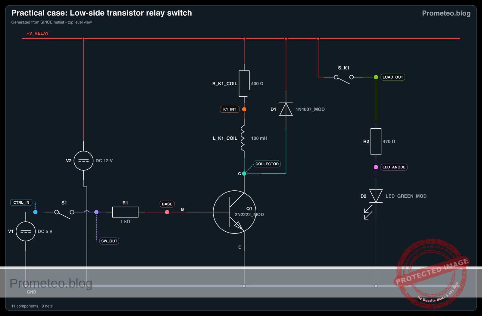
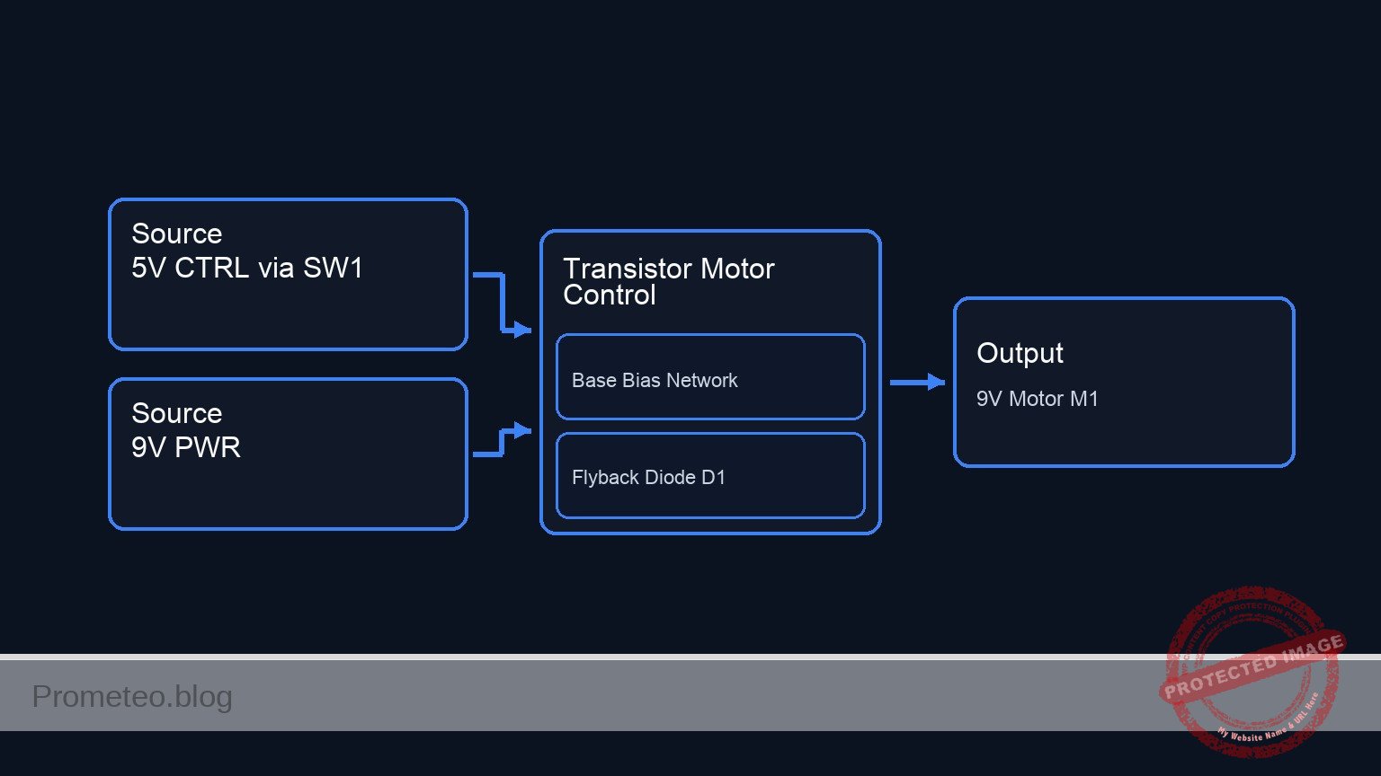
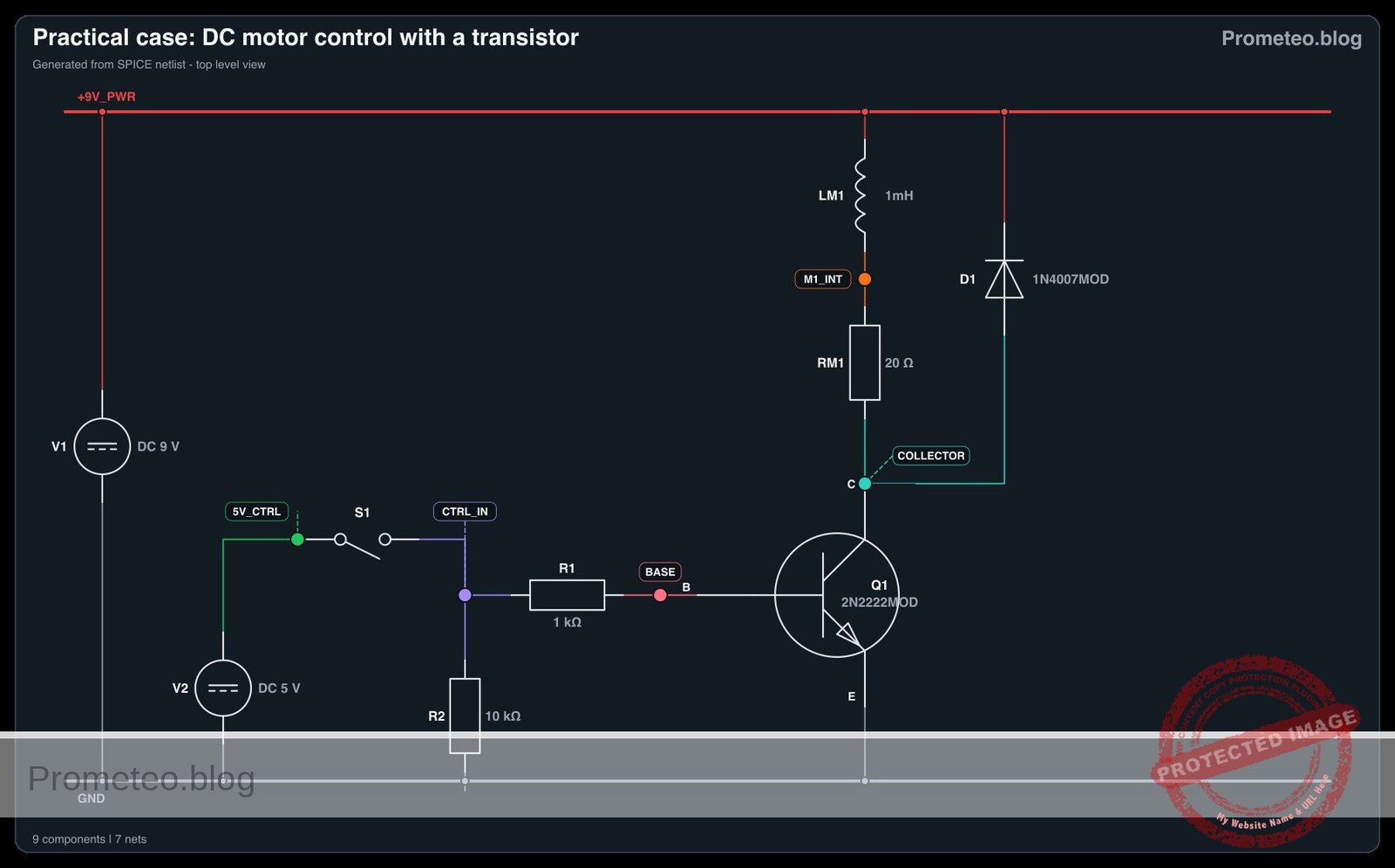
  • V1: 9 V DC supply, function: main power source for the DC motor
  • V2: 5 V DC supply, function: simulated control signal source
  • SW1: SPST switch, function: manual control of the base signal
  • Q1: 2N2222 NPN transistor, function: low-side switch to drive the motor
  • M1: 9 V DC motor, function: inductive mechanical load
  • D1: 1N4007 diode, function: flyback diode to suppress inductive spikes
  • R1: 1 kΩ resistor, function: base current limiting resistor
  • R2: 10 kΩ resistor, function: pull-down resistor for the control signal

Wiring guide

  • V1: connects between nodes 9 V_PWR and 0
  • V2: connects between nodes 5 V_CTRL and 0
  • SW1: connects between nodes 5 V_CTRL and CTRL_IN
  • R2: connects between nodes CTRL_IN and 0
  • R1: connects between nodes CTRL_IN and BASE
  • Q1: Collector connects to node COLLECTOR, Base connects to node BASE, Emitter connects to node 0
  • M1: connects between nodes 9 V_PWR and COLLECTOR
  • D1: Anode connects to node COLLECTOR, Cathode connects to node 9 V_PWR

Conceptual block diagram

Conceptual block diagram — Transistor Motor Control
Quick read: inputs → main block → output (actuator or measurement). This summarizes the ASCII schematic below.

Schematic

[ 5 V_CTRL ] --> [ SW1 ] --(CTRL_IN)--+--> [ R1: 1 kΩ ] --(BASE)--> [ Q1:Base ]
                                           |                                |
                                       [ R2: 10 kΩ ]                         |
                                           |                                |
                                          GND                               |
                                                                            |
      [ 9 V_PWR ] --+--> [ M1: 9 V Motor ] -----------------+--(COLLECTOR)--> [ Q1:Collector ] --( )-- [ Q1:Emitter ] --> GND
                   |                                      |
                   +--> [ D1: 1N4007 (Cath->Anode) ] -----+
Electrical Schematic

Electrical diagram

Electrical diagram for case: DC motor control with a transistor
Generated from the validated SPICE netlist for this case.

🔒 This electrical diagram is premium. With the 7-day pass or the monthly membership you can unlock the complete didactic material and the print-ready PDF pack.🔓 See premium access plans

Measurements and tests

  1. Verify Control Signal: Close SW1. Measure the voltage at node CTRL_IN with respect to node 0. It should read 5 V. When open, it should read 0 V due to the pull-down resistor R2.
  2. Measure Base-Emitter Voltage (VBE): With SW1 closed, place your multimeter probes across node BASE and node 0. You should measure approximately 0.7 V, confirming the transistor’s base-emitter junction is forward-biased.
  3. Measure Collector-Emitter Voltage (VCE): With the motor running (SW1 closed), measure the voltage between node COLLECTOR and node 0. A reading of around 0.2 V indicates the transistor is correctly operating in the saturation region. When SW1 is open, this voltage should rise to 9 V.
  4. Measure Base Current (IB): Set your multimeter to measure current (mA range) and place it in series between R1 and node BASE. You should measure a small current (around 4.3 mA).
  5. Measure Collector Current (IC): Place your ammeter in series between M1 and node COLLECTOR. You will measure the actual current drawn by the motor (which could range from tens to hundreds of mA depending on the specific motor).

SPICE netlist and simulation

Reference SPICE Netlist (ngspice) — excerptFull SPICE netlist (ngspice)

* DC Motor Control with a Transistor
.width out=256

* Power Supplies
V1 9V_PWR 0 DC 9
V2 5V_CTRL 0 DC 5

* Switch SW1 modeled as a voltage-controlled switch to simulate user interaction
S1 5V_CTRL CTRL_IN SW_CTRL 0 mySW
.model mySW SW(Vt=2.5 Vh=0.5 Ron=0.1 Roff=100MEG)

* Control signal to simulate the user pressing the switch
V_SW_CTRL SW_CTRL 0 PULSE(0 5 10m 1u 1u 245m 1s)

* Resistors
R2 CTRL_IN 0 10k
R1 CTRL_IN BASE 1k

* Transistor Q1 (Low-side switch)
Q1 COLLECTOR BASE 0 2N2222MOD
* ... (truncated in public view) ...

Copy this content into a .cir file and run with ngspice.

🔒 Part of this section is premium. With the 7-day pass or the monthly membership you can access the full content (materials, wiring, detailed build, validation, troubleshooting, variants and checklist) and download the complete print-ready PDF pack.

* DC Motor Control with a Transistor
.width out=256

* Power Supplies
V1 9V_PWR 0 DC 9
V2 5V_CTRL 0 DC 5

* Switch SW1 modeled as a voltage-controlled switch to simulate user interaction
S1 5V_CTRL CTRL_IN SW_CTRL 0 mySW
.model mySW SW(Vt=2.5 Vh=0.5 Ron=0.1 Roff=100MEG)

* Control signal to simulate the user pressing the switch
V_SW_CTRL SW_CTRL 0 PULSE(0 5 10m 1u 1u 245m 1s)

* Resistors
R2 CTRL_IN 0 10k
R1 CTRL_IN BASE 1k

* Transistor Q1 (Low-side switch)
Q1 COLLECTOR BASE 0 2N2222MOD

* Motor M1 modeled as a series inductor and resistor representing the inductive mechanical load
LM1 9V_PWR M1_INT 1mH
RM1 M1_INT COLLECTOR 20

* Flyback diode D1
D1 COLLECTOR 9V_PWR 1N4007MOD

* Component Models
.model 2N2222MOD NPN(IS=1E-14 VAF=100 BF=200 IKF=0.3 XTB=1.5 BR=3 CJC=8E-12 CJE=25E-12 TR=100E-9 TF=400E-12 ITF=1 VTF=2 XTF=3 RB=10 RC=0.3 RE=0.2)
.model 1N4007MOD D(IS=7.02767n RS=0.0341512 N=1.80803 EG=1.11 XTI=3.0 BV=1000 IBV=5e-08 CJO=1e-11 VJ=0.7 M=0.5 FC=0.5 TT=1e-07)

* Simulation Commands
.op
.tran 0.1m 250m
.print tran V(CTRL_IN) V(COLLECTOR) V(BASE) I(LM1)
.end

Simulation Results (Transient Analysis)

Simulation Results (Transient Analysis)
Analysis: The simulation shows that when the control signal (v(ctrl_in)) goes high to ~5V at t=10ms, the transistor turns on, pulling the collector voltage down from 9V to ~1.64V. The base voltage rises to ~0.94V, and the motor current (lm1#branch) ramps up to ~368mA, indicating successful motor activation.
Show raw data table (2541 rows)
Index   time            v(ctrl_in)      v(collector)    v(base)         lm1#branch
0	0.000000e+00	5.000400e-04	9.000000e+00	5.000490e-04	1.799750e-11
1	1.000000e-06	5.000400e-04	9.000000e+00	5.000490e-04	1.800624e-11
2	2.000000e-06	5.000400e-04	9.000000e+00	5.000490e-04	1.800815e-11
3	4.000000e-06	5.000400e-04	9.000000e+00	5.000490e-04	1.800528e-11
4	8.000000e-06	5.000400e-04	9.000000e+00	5.000490e-04	1.799050e-11
5	1.600000e-05	5.000400e-04	9.000000e+00	5.000490e-04	1.798412e-11
6	3.200000e-05	5.000400e-04	9.000000e+00	5.000490e-04	1.797999e-11
7	6.400000e-05	5.000400e-04	9.000000e+00	5.000490e-04	1.798801e-11
8	1.280000e-04	5.000400e-04	9.000000e+00	5.000490e-04	1.797977e-11
9	2.280000e-04	5.000400e-04	9.000000e+00	5.000490e-04	1.799637e-11
10	3.280000e-04	5.000400e-04	9.000000e+00	5.000490e-04	1.799685e-11
11	4.280000e-04	5.000400e-04	9.000000e+00	5.000490e-04	1.799640e-11
12	5.280000e-04	5.000400e-04	9.000000e+00	5.000490e-04	1.799689e-11
13	6.280000e-04	5.000400e-04	9.000000e+00	5.000490e-04	1.799636e-11
14	7.280000e-04	5.000400e-04	9.000000e+00	5.000490e-04	1.799685e-11
15	8.280000e-04	5.000400e-04	9.000000e+00	5.000490e-04	1.799639e-11
16	9.280000e-04	5.000400e-04	9.000000e+00	5.000490e-04	1.799690e-11
17	1.028000e-03	5.000400e-04	9.000000e+00	5.000490e-04	1.799645e-11
18	1.128000e-03	5.000400e-04	9.000000e+00	5.000490e-04	1.799690e-11
19	1.228000e-03	5.000400e-04	9.000000e+00	5.000490e-04	1.799640e-11
20	1.328000e-03	5.000400e-04	9.000000e+00	5.000490e-04	1.799689e-11
21	1.428000e-03	5.000400e-04	9.000000e+00	5.000490e-04	1.799641e-11
22	1.528000e-03	5.000400e-04	9.000000e+00	5.000490e-04	1.799690e-11
23	1.628000e-03	5.000400e-04	9.000000e+00	5.000490e-04	1.799640e-11
... (2517 more rows) ...

Common mistakes and how to avoid them

  • Omitting the flyback diode (D1): A DC motor is an inductive load. When the transistor turns off, the collapsing magnetic field creates a massive voltage spike. Without the diode, this spike will instantly destroy the transistor. Always place a diode in parallel with the motor, reverse-biased relative to the normal current flow.
  • Forgetting the base resistor (R1): Connecting a 5 V control signal directly to the transistor’s base will draw excessive current, immediately destroying the control source (e.g., your microcontroller) or the transistor. Always use a current-limiting resistor.
  • Swapping the Collector and Emitter pins: Inserting the NPN transistor backward will result in very poor current gain (hFE). The motor may barely turn, and the transistor will heat up significantly because it cannot fully saturate. Double-check the datasheet for your specific transistor’s pinout.

Troubleshooting

  • Symptom: The motor does not spin when the switch is closed.
    • Cause: The transistor is not turning on, or the motor lacks power.
    • Fix: Measure the voltage at node BASE. If it is 0 V, check your switch SW1 and resistor R1. Measure node 9 V_PWR to ensure the main power supply is active.
  • Symptom: The transistor becomes extremely hot very quickly.
    • Cause: The transistor is operating in the active/linear region instead of fully saturating, usually because the base current (IB) is too low for the required collector current (IC).
    • Fix: Calculate the required base current (IC / hFE). If the current is too low, reduce the value of R1 (e.g., to 470 Ω or 330 Ω) to allow more base current, ensuring saturation.
  • Symptom: The microcontroller resets or behaves erratically when the motor turns on/off.
    • Cause: Electrical noise from the motor brushes or voltage drops on the power line.
    • Fix: Ensure the motor power supply (V1) is completely separate from the control logic supply (V2), sharing only the ground (0) connection. Add a 100 nF ceramic capacitor across the motor terminals to suppress brush noise.

Possible improvements and extensions

  • PWM Speed Control: Replace the manual switch (SW1) with a Pulse Width Modulation (PWM) signal from a microcontroller. By rapidly turning the transistor on and off, you can smoothly control the rotational speed of the motor rather than just having it on or off.
  • Optoisolation for superior safety: Introduce an optocoupler between the control signal and the transistor base. This physically separates the low-voltage control circuit from the higher-voltage motor circuit using light, providing total electrical isolation and preventing catastrophic failures from reaching your logic board.

More Practical Cases on Prometeo.blog

Find this product and/or books on this topic on Amazon

Go to Amazon

As an Amazon Associate, I earn from qualifying purchases. If you buy through this link, you help keep this project running.

Quick Quiz

Question 1: What is the primary objective of the circuit described in the context?


Question 2: What type of switch circuit is built using the NPN transistor in this practical case?


Question 3: Why is this topology useful for microcontrollers like Arduino or Raspberry Pi?


Question 4: What is the purpose of the flyback diode in this circuit?


Question 5: What happens when a 5 V control signal is applied to the base circuit?


Question 6: How does the DC motor spin in this circuit configuration?


Question 7: What is the expected measurable base-emitter voltage (V_BE) when the transistor is saturated?


Question 8: What collector-emitter voltage (V_CE) indicates that the transistor is in saturation?


Question 9: Which of the following is a real-world application mentioned for this circuit?


Question 10: What type of load is a DC motor considered in the context of voltage spikes?


Carlos Núñez Zorrilla
Electronics & Computer Engineer

Telecommunications Electronics Engineer and Computer Engineer (official degrees in Spain).

Follow me:


Practical case: Vault Lock with Delay and Power Drive

Vault Lock with Delay and Power Drive prototype (Maker Style)

Level: Basic. Build a secure electronic lock that keeps a solenoid active for a few seconds after two keys are turned simultaneously.

Objective and use case

In this practical case, you will build a security circuit that requires two distinct inputs (keys/buttons) to be activated simultaneously to trigger a high-power mechanism. Once triggered, the system includes an analog memory (RC network) to hold the lock open for a short duration, allowing a user to open the door.

  • Real-world scenarios:

    • Bank Vaults: Requires two bank managers to turn keys at the same time to prevent theft.
    • Industrial Presses: Requires an operator to press buttons with both hands to ensure safety before the machine engages.
    • Secure Entryways: Allows a door strike to remain unlatched for 5 seconds after authorization.
  • Expected outcome:

    • Logic: The load (Solenoid/LED) remains OFF if only one button is pressed.
    • Activation: The load turns ON fully only when both SW1 and SW2 are held.
    • Timing: Upon releasing the buttons, the load remains ON for approximately 2 to 5 seconds before fading out.
    • Target audience: Basic electronics students focusing on transistor switching and RC time constants.

Materials

  • V1: 12 V DC supply, function: Main power source.
  • SW1: Push button (Normally Open), function: Security Key 1.
  • SW2: Push button (Normally Open), function: Security Key 2.
  • R1: 1 kΩ resistor, function: Current limiter for capacitor charging (protection).
  • R2: 47 kΩ resistor, function: Discharge timing resistor (Bleeder).
  • C1: 100 µF electrolytic capacitor, function: Energy storage for time delay.
  • Q1: IRF540 N-Channel MOSFET, function: Power switch for the load.
  • L1: 10 mH inductor, function: Solenoid coil simulation.
  • R3: 10 Ω resistor, function: Internal resistance of the solenoid.
  • D1: 1N4007 Diode, function: Flyback protection against inductive voltage spikes.

Wiring guide

This guide uses the node names 12 V, 0 (Ground), Mid_Switch, Gate_Node, and Drain_Node.

  • Logic Stage (Series AND):

    • V1 (Positive) connects to SW1 (Input).
    • SW1 (Output) connects to Mid_Switch.
    • SW2 (Input) connects to Mid_Switch.
    • SW2 (Output) connects to R1 (Input).
  • Timing Stage (RC Hold):

    • R1 (Output) connects to Gate_Node.
    • C1 (Positive) connects to Gate_Node.
    • C1 (Negative) connects to 0.
    • R2 connects between Gate_Node and 0 (Parallel to C1).
    • Q1 (Gate) connects to Gate_Node.
  • Power Stage:

    • Q1 (Source) connects to 0.
    • Q1 (Drain) connects to Drain_Node.
    • L1 and R3 (representing the Solenoid) are connected in series between 12 V and Drain_Node.
    • D1 (Cathode) connects to 12 V.
    • D1 (Anode) connects to Drain_Node (across the load).

Conceptual block diagram

Conceptual block diagram — CD40106 Transistor
Quick read: inputs → main block → output (actuator or measurement). This summarizes the ASCII schematic below.

Schematic

Title: Practical case: Vault Lock with Delay and Power Drive

(1) LOGIC & TIMING STAGE
------------------------
                                                                    (Gate_Node)
[ 12 V ] --(Logic)--> [ SW1 ] --> [ SW2 ] --> [ R1: 1k ] --+------------+----------> [ Q1:Gate ]
                                                          |            |                |
                                                          |            |                |
                                                          v            v                |
                                                    [ C1: 100uF ]  [ R2: 47k ]          |
                                                          |            |                |
                                                          v            v                |
                                                         GND          GND               |
                                                                                        |
(2) POWER DRIVE STAGE                                                                   |
---------------------                                                                   |
                                                                                        |
[ 12 V ] --(Power)-----------------------------------------+                             |
   |                                                      |                             |
   |                                                      v                             |
   |                                              [ Solenoid (L1+R3) ]                  |
   |                                                      |                             |
   |                                                      v                             |
   +----(Cathode)-- [ D1: Flyback ] --(Anode)----> (Drain_Node) ----> [ Q1:Drain ]      |
                                                                            |           |
                                                                            +-----------+
                                                                            |
                                                                      (Internal FET)
                                                                            |
                                                                            v
                                                                      [ Q1:Source ]
                                                                            |
                                                                            v
                                                                           GND
Electrical Schematic

Electrical diagram

Electrical diagram for case: Vault lock with delay and power drive
Generated from the validated SPICE netlist for this case.

🔒 This electrical diagram is premium. With the 7-day pass or the monthly membership you can unlock the complete didactic material and the print-ready PDF pack.🔓 See premium access plans

Measurements and tests

Validate the circuit operation using a multimeter or oscilloscope:

  1. Logic Verification: Press SW1 only. Measure voltage at Gate_Node. It should be 0 V. Repeat for SW2 only. The load should remain OFF.
  2. Activation: Press SW1 and SW2 simultaneously. Measure voltage at Gate_Node. It should rise immediately to approx 12 V. The Solenoid (Load) should activate.
  3. Hold Time (Delay): Release both buttons simultaneously. Watch the load.
    • The voltage at Gate_Node will begin to drop.
    • The Solenoid should remain active.
    • Measure the time it takes for the load to turn off (typically when Gate voltage drops below the MOSFET Threshold, ~3-4 V). With 47 kΩ and 100µF, this should be roughly 3 to 5 seconds.
  4. Flyback Check: (Oscilloscope only) Monitor Drain_Node when the transistor turns off. You should not see a massive voltage spike above 12 V, confirming D1 is clamping the inductive kickback.

SPICE netlist and simulation

Reference SPICE Netlist (ngspice) — excerptFull SPICE netlist (ngspice)

* Practical case: Vault Lock with Delay and Power Drive
.width out=256

* --- Models ---
* Generic Switch Model for Push Buttons
.model SW_push SW(Vt=2.5 Ron=0.01 Roff=100Meg)

* Power MOSFET Model (Approximation of IRF540)
* N-Channel, Threshold ~4V, Low Rds(on)
.model IRF540 NMOS(Level=1 Vto=4.0 Kp=20 Lambda=0.001 Rd=0.05 Rs=0.05)

* Diode Model (1N4007)
.model D1N4007 D(Is=14.11n N=1.984 Rs=33.89m Ikf=100m Cjo=20p M=0.3333 Vj=0.75 Bv=1000 Ibv=10u)

* --- Main Power Supply ---
V1 12V 0 DC 12

* --- User Interface (Push Buttons) ---
* We simulate physical button presses using Pulse Voltage Sources controlling switches.
* Logic: To unlock, SW1 and SW2 must be pressed simultaneously (AND logic).
* ... (truncated in public view) ...

Copy this content into a .cir file and run with ngspice.

🔒 Part of this section is premium. With the 7-day pass or the monthly membership you can access the full content (materials, wiring, detailed build, validation, troubleshooting, variants and checklist) and download the complete print-ready PDF pack.

* Practical case: Vault Lock with Delay and Power Drive
.width out=256

* --- Models ---
* Generic Switch Model for Push Buttons
.model SW_push SW(Vt=2.5 Ron=0.01 Roff=100Meg)

* Power MOSFET Model (Approximation of IRF540)
* N-Channel, Threshold ~4V, Low Rds(on)
.model IRF540 NMOS(Level=1 Vto=4.0 Kp=20 Lambda=0.001 Rd=0.05 Rs=0.05)

* Diode Model (1N4007)
.model D1N4007 D(Is=14.11n N=1.984 Rs=33.89m Ikf=100m Cjo=20p M=0.3333 Vj=0.75 Bv=1000 Ibv=10u)

* --- Main Power Supply ---
V1 12V 0 DC 12

* --- User Interface (Push Buttons) ---
* We simulate physical button presses using Pulse Voltage Sources controlling switches.
* Logic: To unlock, SW1 and SW2 must be pressed simultaneously (AND logic).
V_act1 Ctrl1 0 PULSE(0 5 1 1m 1m 3 10)
V_act2 Ctrl2 0 PULSE(0 5 2.5 1m 1m 3 10)

* --- Logic Stage (Series AND) ---
* SW1 connects 12V to Mid_Switch
S1 12V Mid_Switch Ctrl1 0 SW_push

* SW2 connects Mid_Switch to R1 Input
S2 Mid_Switch Pre_R1 Ctrl2 0 SW_push

* --- Timing Stage (RC Hold) ---
* R1: Current limiter for charging
R1 Pre_R1 Gate_Node 1k

* C1: Energy storage (Timing capacitor)
C1 Gate_Node 0 100u

* R2: Discharge timing resistor (Bleeder)
* Time Constant (Discharge) = 47k * 100u = 4.7 seconds
R2 Gate_Node 0 47k

* --- Power Stage ---
* Q1 renamed to M1 to match SPICE MOSFET syntax (requires M prefix for NMOS model).
* Pin order: Drain Gate Source Bulk. Bulk connected to Source (0).
M1 Drain_Node Gate_Node 0 0 IRF540

* --- Load (Solenoid Simulation) ---
* Modeled as Inductor L1 and Resistor R3 in series
L1 12V Solenoid_Mid 10mH
R3 Solenoid_Mid Drain_Node 10

* --- Protection ---
* D1: Flyback diode to suppress inductive spikes from L1 upon turn-off
* Connected Cathode to 12V, Anode to Drain
D1 Drain_Node 12V D1N4007

* --- Simulation Commands ---
.op
* Transient analysis: 10ms step for 10 seconds to capture full charge/discharge cycle
.tran 10m 10s

* --- Output ---
* Monitoring Control signals, Gate voltage (Timing), and Drain voltage (Output state)
.print tran V(Ctrl1) V(Ctrl2) V(Gate_Node) V(Drain_Node) I(L1)

.end

Simulation Results (Transient Analysis)

Simulation Results (Transient Analysis)

Analysis: The simulation confirms the intended operation. When the control signals activate the series switches (AND logic), the gate node charges to ~11.7V, turning the MOSFET ON (Drain drops to ~0.13V, Current ~1.18A). After the input pulses cease, the gate voltage decays slowly via R2. Around 9 seconds into the simulation, the gate voltage drops near the threshold (4V), and the MOSFET turns off, returning the Drain voltage to 12V.
Show raw data table (1095 rows)
Index   time            v(ctrl1)        v(ctrl2)        v(gate_node)    v(drain_node)   l1#branch
0	0.000000e+00	0.000000e+00	0.000000e+00	2.819323e-03	1.200000e+01	1.199844e-11
1	1.000000e-04	0.000000e+00	0.000000e+00	2.819323e-03	1.200000e+01	1.204503e-11
2	2.000000e-04	0.000000e+00	0.000000e+00	2.819323e-03	1.200000e+01	1.196043e-11
3	4.000000e-04	0.000000e+00	0.000000e+00	2.819323e-03	1.200000e+01	1.204260e-11
4	8.000000e-04	0.000000e+00	0.000000e+00	2.819323e-03	1.200000e+01	1.204346e-11
5	1.600000e-03	0.000000e+00	0.000000e+00	2.819323e-03	1.200000e+01	1.201220e-11
6	3.200000e-03	0.000000e+00	0.000000e+00	2.819323e-03	1.200000e+01	1.199165e-11
7	6.400000e-03	0.000000e+00	0.000000e+00	2.819323e-03	1.200000e+01	1.202979e-11
8	1.280000e-02	0.000000e+00	0.000000e+00	2.819323e-03	1.200000e+01	1.202182e-11
9	2.280000e-02	0.000000e+00	0.000000e+00	2.819323e-03	1.200000e+01	1.199840e-11
10	3.280000e-02	0.000000e+00	0.000000e+00	2.819323e-03	1.200000e+01	1.200551e-11
11	4.280000e-02	0.000000e+00	0.000000e+00	2.819323e-03	1.200000e+01	1.199929e-11
12	5.280000e-02	0.000000e+00	0.000000e+00	2.819323e-03	1.200000e+01	1.200551e-11
13	6.280000e-02	0.000000e+00	0.000000e+00	2.819323e-03	1.200000e+01	1.199929e-11
14	7.280000e-02	0.000000e+00	0.000000e+00	2.819323e-03	1.200000e+01	1.200551e-11
15	8.280000e-02	0.000000e+00	0.000000e+00	2.819323e-03	1.200000e+01	1.199929e-11
16	9.280000e-02	0.000000e+00	0.000000e+00	2.819323e-03	1.200000e+01	1.200551e-11
17	1.028000e-01	0.000000e+00	0.000000e+00	2.819323e-03	1.200000e+01	1.199929e-11
18	1.128000e-01	0.000000e+00	0.000000e+00	2.819323e-03	1.200000e+01	1.200551e-11
19	1.228000e-01	0.000000e+00	0.000000e+00	2.819323e-03	1.200000e+01	1.199929e-11
20	1.328000e-01	0.000000e+00	0.000000e+00	2.819323e-03	1.200000e+01	1.200551e-11
21	1.428000e-01	0.000000e+00	0.000000e+00	2.819323e-03	1.200000e+01	1.199929e-11
22	1.528000e-01	0.000000e+00	0.000000e+00	2.819323e-03	1.200000e+01	1.200551e-11
23	1.628000e-01	0.000000e+00	0.000000e+00	2.819323e-03	1.200000e+01	1.199929e-11
... (1071 more rows) ...

Common mistakes and how to avoid them

  1. Omitting the Flyback Diode (D1):
    • Error: The MOSFET fails after a few cycles due to high voltage spikes from the solenoid.
    • Solution: Always place a diode in parallel with inductive loads, cathode to positive supply.
  2. Wrong Capacitor Polarity:
    • Error: C1 explodes or heats up; circuit acts as a short.
    • Solution: Ensure the negative stripe of the electrolytic capacitor connects to Ground (0).
  3. Gate Floating:
    • Error: If R2 is removed, the lock stays stuck «ON» indefinitely because the gate charge has nowhere to go.
    • Solution: Ensure R2 is connected between Gate and Ground to provide a discharge path.

Troubleshooting

  • Solenoid turns off instantly (No delay):
    • Cause: C1 is too small, damaged, or R2 is too low (e.g., 1 kΩ instead of 47 kΩ).
    • Fix: Check R2 value or increase C1 capacitance.
  • MOSFET gets very hot during the «OFF» transition:
    • Cause: Slow discharge causes the MOSFET to linger in the «linear region» (acting as a resistor) for too long.
    • Fix: This is expected in simple RC delay circuits. Ensure the MOSFET has a heatsink or switch to a Logic-based delay (Schmitt Trigger) for a sharper cutoff.
  • Circuit never activates:
    • Cause: SW1 and SW2 are not wired in series, or MOSFET pinout (G-D-S) is incorrect.
    • Fix: Verify continuity through the switches to the Gate pin.

Possible improvements and extensions

  1. Schmitt Trigger Snap-Action: Insert a Schmitt Trigger inverter (like CD40106) between the RC network and the MOSFET. This creates a clean, digital ON/OFF transition, preventing the MOSFET from heating up during the discharge phase.
  2. Emergency Reset: Add a «Panic» switch (Normally Closed) in parallel with the capacitor C1. Pressing it instantly shorts the capacitor, locking the vault immediately regardless of the remaining time.

More Practical Cases on Prometeo.blog

Find this product and/or books on this topic on Amazon

Go to Amazon

As an Amazon Associate, I earn from qualifying purchases. If you buy through this link, you help keep this project running.

Quick Quiz

Question 1: What is the primary condition required to activate the load in this security circuit?


Question 2: Which component acts as the 'analog memory' to keep the lock open for a short duration?


Question 3: What is a real-world application mentioned for this type of dual-input security circuit?


Question 4: What is the function of the IRF540 (Q1) in this circuit?


Question 5: What happens to the load immediately after the buttons are released?


Question 6: Which component is generally responsible for limiting the current while the capacitor charges in this type of RC circuit?


Question 7: What is the specific role of the discharge resistor (e.g., R2) in the circuit?


Question 8: Based on the context, what type of capacitor is typically used for timing circuits requiring values like 100 µF?


Question 9: Why might an industrial press use a circuit logic similar to this project?


Question 10: What is the specified voltage source for the main power supply in the context provided?


Carlos Núñez Zorrilla
Electronics & Computer Engineer

Telecommunications Electronics Engineer and Computer Engineer (official degrees in Spain).

Follow me:


Practical case: The Undefined Logic Level Danger

The Undefined Logic Level Danger prototype (Maker Style)

Level: Basic. Analyzing the instability caused by improper voltage divider inputs on digital gates.

Objective and use case

In this practical case, you will build a circuit where the input to a digital inverter (NOT gate) is held at exactly 2.5 V using a symmetrical voltage divider. This creates a «forbidden» state for 5 V logic families.

  • Understanding Logic Thresholds: Learn why digital inputs need defined High and Low voltages, not just «something in the middle.»
  • Diagnosing Instability: Recognize symptoms of undefined states, such as oscillation or excessive heating.
  • Internal Transistor Behavior: Visualize what happens to the internal MOSFETs when the input voltage is in the «dead zone.»

Expected Outcome:
* Signal: The input voltage (Vin) measures exactly 2.5 V.
* Output: The Output LED may be dim, flickering, or stuck at an intermediate voltage (not fully 0 V or 5 V).
* Thermal: The 74HC04 chip may become slightly warm due to internal «shoot-through» current.

Target audience: Students dealing with sensor interfacing and logic levels.

Materials

  • V1: 5 V DC supply, function: Main power source
  • R1: 10 kΩ resistor, function: Top leg of voltage divider
  • R2: 10 kΩ resistor, function: Bottom leg of voltage divider
  • U1: 74HC04, function: Hex Inverter (NOT gate)
  • R3: 330 Ω resistor, function: LED current limiting
  • D1: Red LED, function: Logic state indicator
  • C1: 100 nF capacitor, function: Power supply decoupling

Pin-out of the IC used

Chip: 74HC04 (Hex Inverter)

Pin Name Logic Function Connection in this case
1 1 A Input Connected to Voltage Divider (2.5 V)
2 1Y Output Connected to LED resistor
7 GND Ground Connected to Power Supply Ground
14 VCC Power (+5 V) Connected to Power Supply +5 V

Wiring guide

  • VCC: Connect positive terminal of V1, Pin 14 of U1, and one side of R1.
  • 0 (GND): Connect negative terminal of V1, Pin 7 of U1, one side of R2, and the cathode (short leg) of D1.
  • V_IN: Connect the remaining side of R1, the remaining side of R2, and Pin 1 (Input 1 A) of U1. Note: This node creates the problematic 2.5 V level.
  • V_OUT: Connect Pin 2 (Output 1Y) of U1 to one side of R3.
  • LED_NODE: Connect the remaining side of R3 to the anode (long leg) of D1.
  • Decoupling: Connect C1 directly between Pin 14 and Pin 7 of U1.

Conceptual block diagram

Conceptual block diagram — 74HC04 Transistor
Quick read: inputs → main block → output (actuator or measurement). This summarizes the ASCII schematic below.

Schematic

INPUT STAGE (Voltage Divider)              PROCESSING STAGE (Logic)                  OUTPUT STAGE (Load)

VCC (5 V)
   |
[ R1: 10 kΩ ]
   |
   +---------(V_IN: ~2.5 V)---------> [ U1: 74HC04 (Inverter) ] -------(V_OUT)-------> [ R3: 330 Ω ] ----> [ D1: LED ] ----> GND
   |          (Undefined Level)      [ Input: Pin 1          ]
[ R2: 10 kΩ ]                         [ Output: Pin 2         ]
   |                                 [ Power: VCC/GND + C1   ]
GND (0 V)
Electrical Schematic

Electrical diagram

Electrical diagram for case: The undefined logic level danger
Generated from the validated SPICE netlist for this case.

🔒 This electrical diagram is premium. With the 7-day pass or the monthly membership you can unlock the complete didactic material and the print-ready PDF pack.🔓 See premium access plans

Truth table

Gate: NOT (Inverter)

Input (A) Output (Y)
L (0 V) H (5 V)
H (5 V) L (0 V)
2.5 V Undefined / Unstable

Measurements and tests

  1. Input Voltage Check: Set your multimeter to DC Voltage. Place the red probe on node V_IN (Pin 1 of U1) and the black probe on GND. Verify the reading is approximately 2.5 V.
  2. Output Observation: Look at D1. It might be glowing dimly or flickering. This indicates the output is not driving a solid Logic High or Low.
  3. Output Voltage Check: Measure the voltage at V_OUT (Pin 2). It will likely not be 0 V or 5 V, but a value in between, or it may be oscillating (fluctuating reading).
  4. Touch Test (Caution): Carefully touch the top of the plastic package of the 74HC04. If the chip feels warmer than ambient temperature, it is drawing excess current.

SPICE netlist and simulation

Reference SPICE Netlist (ngspice) — excerptFull SPICE netlist (ngspice)

* Practical case: The Undefined Logic Level Danger
.width out=256

* --- Models ---
* Generic Red LED Model
.model LED_RED D(IS=1e-22 N=1.5 RS=10 BV=5 CJO=50p IBV=1u)

* Subcircuit for U1: 74HC04 Hex Inverter
* Pinout: 1=Input(A), 2=Output(Y), 7=GND, 14=VCC
* Implemented with a continuous sigmoid function to allow robust simulation 
* of the linear region (undefined state) without convergence issues.
.subckt 74HC04 1 2 7 14
B_INV 2 7 V = V(14,7) / (1 + exp(20 * (V(1,7) - 0.5*V(14,7))))
.ends

* --- Components ---

* V1: Main Power Supply
* Using PULSE to simulate power-on transient (0V to 5V)
V1 VCC 0 PULSE(0 5 1u 10u 10u 100m 200m)
* ... (truncated in public view) ...

Copy this content into a .cir file and run with ngspice.

🔒 Part of this section is premium. With the 7-day pass or the monthly membership you can access the full content (materials, wiring, detailed build, validation, troubleshooting, variants and checklist) and download the complete print-ready PDF pack.

* Practical case: The Undefined Logic Level Danger
.width out=256

* --- Models ---
* Generic Red LED Model
.model LED_RED D(IS=1e-22 N=1.5 RS=10 BV=5 CJO=50p IBV=1u)

* Subcircuit for U1: 74HC04 Hex Inverter
* Pinout: 1=Input(A), 2=Output(Y), 7=GND, 14=VCC
* Implemented with a continuous sigmoid function to allow robust simulation 
* of the linear region (undefined state) without convergence issues.
.subckt 74HC04 1 2 7 14
B_INV 2 7 V = V(14,7) / (1 + exp(20 * (V(1,7) - 0.5*V(14,7))))
.ends

* --- Components ---

* V1: Main Power Supply
* Using PULSE to simulate power-on transient (0V to 5V)
V1 VCC 0 PULSE(0 5 1u 10u 10u 100m 200m)

* R1: Top leg of voltage divider (10k)
R1 VCC V_IN 10k

* R2: Bottom leg of voltage divider (10k)
* This creates approx 2.5V at V_IN when VCC is 5V
R2 V_IN 0 10k

* U1: 74HC04 Hex Inverter
* Connections: Pin 1=V_IN, Pin 2=V_OUT, Pin 7=0(GND), Pin 14=VCC
XU1 V_IN V_OUT 0 VCC 74HC04

* C1: Decoupling capacitor (100nF)
C1 VCC 0 100n

* R3: LED current limiting resistor (330 Ohm)
R3 V_OUT LED_NODE 330

* D1: Red LED
D1 LED_NODE 0 LED_RED

* --- Analysis ---

* Transient analysis to capture power-up and settling
* Step size 1us, Stop time 500us
.tran 1u 500u

* Print directives for simulation logging
.print tran V(V_IN) V(V_OUT) V(LED_NODE) V(VCC)

* Operating point calculation
.op

.end

Simulation Results (Transient Analysis)

Simulation Results (Transient Analysis)

Analysis: The simulation shows V_IN settling at exactly 2.5V (half of VCC). The inverter output V_OUT also settles at 2.5V, causing the LED node to sit at ~1.75V. This confirms the ‘undefined’ behavior where the output is neither clearly High nor Low.
Show raw data table (519 rows)
Index   time            v(v_in)         v(v_out)        v(led_node)     v(vcc)
0	0.000000e+00	0.000000e+00	0.000000e+00	-1.32954e-36	0.000000e+00
1	1.000000e-08	0.000000e+00	0.000000e+00	-8.37118e-37	0.000000e+00
2	2.000000e-08	0.000000e+00	0.000000e+00	-2.17031e-37	0.000000e+00
3	4.000000e-08	0.000000e+00	0.000000e+00	6.442019e-37	0.000000e+00
4	8.000000e-08	0.000000e+00	0.000000e+00	1.087387e-36	0.000000e+00
5	1.600000e-07	0.000000e+00	0.000000e+00	5.886649e-37	0.000000e+00
6	3.200000e-07	0.000000e+00	0.000000e+00	-7.16419e-38	0.000000e+00
7	6.400000e-07	0.000000e+00	0.000000e+00	-1.33719e-37	0.000000e+00
8	1.000000e-06	0.000000e+00	0.000000e+00	-1.75658e-38	0.000000e+00
9	1.005123e-06	1.280776e-03	1.280776e-03	3.255392e-04	2.561552e-03
10	1.015369e-06	3.842328e-03	3.842328e-03	1.418765e-03	7.684656e-03
11	1.035862e-06	8.965432e-03	8.965432e-03	5.258943e-03	1.793086e-02
12	1.070382e-06	1.759552e-02	1.759552e-02	1.345000e-02	3.519104e-02
13	1.105069e-06	2.626716e-02	2.626716e-02	2.210557e-02	5.253431e-02
14	1.174442e-06	4.361042e-02	4.361042e-02	3.941132e-02	8.722085e-02
15	1.313188e-06	7.829696e-02	7.829696e-02	7.402122e-02	1.565939e-01
16	1.590680e-06	1.476700e-01	1.476700e-01	1.432281e-01	2.953401e-01
17	2.145665e-06	2.864162e-01	2.864162e-01	2.815810e-01	5.728324e-01
18	3.145665e-06	5.364162e-01	5.364162e-01	5.305352e-01	1.072832e+00
19	4.145665e-06	7.864162e-01	7.864162e-01	7.789169e-01	1.572832e+00
20	5.145665e-06	1.036416e+00	1.036416e+00	1.027633e+00	2.072832e+00
21	6.145665e-06	1.286416e+00	1.286416e+00	1.276050e+00	2.572832e+00
22	7.145665e-06	1.536416e+00	1.536416e+00	1.521539e+00	3.072832e+00
23	8.145665e-06	1.786416e+00	1.786416e+00	1.662480e+00	3.572832e+00
... (495 more rows) ...

Common mistakes and how to avoid them

  1. Assuming 2.5 V is «High»: Many students think any voltage > 0 V is «High.» Check the datasheet for VIH (Voltage Input High) minimum requirements (usually ~3.5 V for 5 V HC logic).
  2. Using High Impedance Dividers: Using 10 kΩ/10 kΩ is fine for references, but noise can easily couple into this high impedance node, causing the gate to switch randomly.
  3. Ignoring Decoupling Capacitors: In this unstable state, the chip generates noise on the power rails. Omitting C1 makes the behavior even more erratic.

Troubleshooting

  • Symptom: The LED is dim or flickering rapidly.
    • Cause: The input is in the «linear region» or «forbidden zone.» The internal transistors are amplifying noise.
    • Fix: Adjust the input voltage to be clearly valid (e.g., tie Input to VCC or GND directly to test).
  • Symptom: The chip is getting hot, but the LED works.
    • Cause: Shoot-through current. Inside the chip, both the P-MOSFET and N-MOSFET of the input stage are partially conducting because 2.5 V biases both of them ON. This creates a short circuit from VCC to GND inside the silicon.
    • Fix: Never leave a CMOS input at an intermediate voltage.
  • Symptom: Voltage at V_IN is not exactly 2.5 V.
    • Cause: Resistor tolerance (e.g., 5% or 10% resistors) or multimeter loading.
    • Fix: Measure R1 and R2 values independently or verify with a precision multimeter.
🕵️ See Diagnosis and Solution (Click to reveal)

### Diagnosis and Solution

**1. The Problem (Symptom):** «The LED flickers, is dim, or the chip heats up. The input measures 2.5 V. Is that a 1 or a 0?»

**2. The Investigation:** You measure Vin and confirm it is 2.5 V. You consult the 74HC04 datasheet:
* VIL (Max Input Low) = 1.35 V
* VIH (Min Input High) = 3.15 V
* **Result:** You are in «No Man’s Land»! The voltage is higher than a Low, but lower than a High.

**3. The Revelation:** This demonstrates **Noise Margins** and Transistor Physics. At 2.5 V, both the internal Input PMOS and NMOS transistors are partially turned ON. This creates a direct path for current to flow from VCC to GND (Shoot-through), causing heat. The output becomes unpredictable and sensitive to even millivolts of noise.

**4. The Solution:** Modify the divider to deliver a safe logic level.
* **To send a ‘1’:** Change **R1 to 1 kΩ** (and keep R2 at 10k). Vout ≈ 4.5 V (Solid Logic High).
* **To send a ‘0’:** Change **R2 to 1 kΩ** (and keep R1 at 10k). Vout ≈ 0.45 V (Solid Logic Low).

Possible improvements and extensions

  1. Hysteresis implementation: Replace the 74HC04 with a 74HC14 (Schmitt Trigger Inverter). Observe how the Schmitt trigger handles the 2.5 V input (it will stay in the previous state until a specific threshold is crossed) without oscillating.
  2. Variable Input: Replace the fixed resistors R1/R2 with a 10 kΩ potentiometer. Sweep the voltage from 0 V to 5 V while measuring the supply current (Amperage). You will see a spike in current exactly around the 2.5 V transition point.

More Practical Cases on Prometeo.blog

Find this product and/or books on this topic on Amazon

Go to Amazon

As an Amazon Associate, I earn from qualifying purchases. If you buy through this link, you help keep this project running.

Quick Quiz

Question 1: What is the main objective of the practical case described in the article?


Question 2: What specific voltage is the input to the NOT gate held at in this experiment?


Question 3: Which specific chip is used as the digital inverter (NOT gate) in this circuit?


Question 4: What is the function of the resistors forming the voltage divider in this circuit?


Question 5: What is a likely symptom of the output LED when the input is in the 'forbidden' zone?


Question 6: Why might the 74HC04 chip become slightly warm during this experiment?


Question 7: What logic family concept is this experiment primarily trying to teach?


Question 8: In a standard 74HC04 pinout, which pin is typically an input (like 1 A) where the divider would connect?


Question 9: Although not explicitly detailed in the text, what is the standard function of a 100 nF capacitor (C1) in digital circuits like this?


Question 10: What happens to the internal MOSFETs when the input voltage is in the 'dead zone'?


Carlos Núñez Zorrilla
Electronics & Computer Engineer

Telecommunications Electronics Engineer and Computer Engineer (official degrees in Spain).

Follow me:


Practical case: NPN Switch Saturation Troubleshooting

NPN Switch Saturation Troubleshooting prototype (Maker Style)

Level: Basic. Learn to identify and fix an NPN transistor stuck in the active region.

Objective and use case

In this practical case, you will build a standard Low-Side Switch using a BJT (Bipolar Junction Transistor) to control a high-current load. However, the circuit will contain a deliberate flaw in the base resistor selection to demonstrate the difference between the Active Region and Saturation.

  • Understanding Transistor Modes: Learn why a transistor acts as a resistor instead of a switch if not biased correctly.
  • Power Dissipation: Understand why partially open transistors overheat.
  • Troubleshooting: Practice measuring VCE to diagnose switching efficiency.

Expected outcome:
* Initially, the high-current LED will be surprisingly dim.
* Voltage measurement across the transistor (VCE) will be high (> 2 V).
* After the fix, the LED will be bright, and VCE will drop to near 0 V.
* Target audience: Beginners and students familiar with basic Ohm’s Law.

Materials

  • V1: 5 V DC Power Supply, function: Main circuit power.
  • Q1: 2N2222 NPN Transistor, function: Low-side switch.
  • D1: High-Brightness White LED, function: The heavy load (requires approx. 80-100 mA).
  • R1: 33 Ω resistor (1/2 Watt), function: LED current limiting (Rload).
  • R2: 100 kΩ resistor, function: Incorrect Base resistor (Test Case).
  • R3: 1 kΩ resistor, function: Correct Base resistor (Solution).
  • S1: SPST Switch or Jumper wire, function: Input control.

Wiring guide

Construct the circuit using the following netlist connections. Pay attention to the node names.

  • V1 (5 V) connects to node VCC.
  • V1 (GND) connects to node 0.
  • S1 connects between VCC and node SWITCH_OUT.
  • R2 (100 kΩ) connects between SWITCH_OUT and node BASE.
  • Q1 Base connects to node BASE.
  • Q1 Emitter connects to node 0 (GND).
  • Q1 Collector connects to node COLLECTOR.
  • D1 Anode connects to node VCC.
  • D1 Cathode connects to node LED_CATHODE.
  • R1 (33 Ω) connects between LED_CATHODE and COLLECTOR.

Conceptual block diagram

Conceptual block diagram — NPN Switch (Saturation Test)
Quick read: inputs → main block → output (actuator or measurement). This summarizes the ASCII schematic below.

Schematic

Title: Practical case: NPN Switch Saturation Troubleshooting

(1) CONTROL PATH (Base Current Drive)
    VCC --> [ S1: Switch ] --(SWITCH_OUT)--> [ R2: 100k ] --(BASE)--> [ Q1: Base ]
                                                                           |
                                                                    (Activates Switch)
                                                                           |
                                                                           V

(2) POWER PATH (High Current Load)
    VCC --> [ D1: LED ] --(LED_CATHODE)--> [ R1: 33 Ohm ] --(COLLECTOR)--> [ Q1: Collector ]
                                                                                 |
                                                                           (Current Flow)
                                                                                 |
                                                                                 V
                                                                           [ Q1: Emitter ] --> GND
Electrical Schematic

Electrical diagram

Electrical diagram for case: NPN switch saturation troubleshooting
Generated from the validated SPICE netlist for this case.

🔒 This electrical diagram is premium. With the 7-day pass or the monthly membership you can unlock the complete didactic material and the print-ready PDF pack.🔓 See premium access plans

Measurements and tests

Follow this procedure to analyze the circuit behavior before applying the fix.

  1. Visual Inspection: Close switch S1. Observe the brightness of D1. It should be noticeably dim for a high-brightness LED.
  2. Base Voltage Check: Measure voltage at node BASE relative to GND. It should be approximately 0.7 V.
  3. Collector Voltage (VCE) Check: Measure voltage at node COLLECTOR relative to GND (across the transistor).
    • Expectation for a perfect switch: ~0 V.
    • Actual measurement: You will likely measure a significant voltage (e.g., 2 V to 4 V depending on the exact gain of your specific Q1).
  4. Calculated Current: Calculate the current entering the base: IB = (5 V – 0.7 V) / 100 kΩ.

SPICE netlist and simulation

Reference SPICE Netlist (ngspice) — excerptFull SPICE netlist (ngspice)

* Practical case: NPN Switch Saturation Troubleshooting
.width out=256

* --- Power Supply ---
V1 VCC 0 DC 5

* --- Input Control (S1) ---
* S1 connects VCC to SWITCH_OUT. Modeled as a voltage-controlled switch
* driven by a PULSE source to simulate user actuation.
S1 VCC SWITCH_OUT CTRL 0 SW_IDEAL
Vctrl CTRL 0 PULSE(0 5 0 1u 1u 50u 100u)
.model SW_IDEAL SW(Vt=2.5 Ron=0.01 Roff=100Meg)

* --- Circuit Components ---
* R2: Incorrect Base resistor (100k) causing weak saturation.
* This matches the "Troubleshooting" state defined in the Wiring Guide.
R2 SWITCH_OUT BASE 100k

* Note: R3 (1k) is listed in the BOM as the 'Solution' but is not connected
* in the current wiring guide configuration. It is omitted to prevent floating nodes.
* ... (truncated in public view) ...

Copy this content into a .cir file and run with ngspice.

🔒 Part of this section is premium. With the 7-day pass or the monthly membership you can access the full content (materials, wiring, detailed build, validation, troubleshooting, variants and checklist) and download the complete print-ready PDF pack.

* Practical case: NPN Switch Saturation Troubleshooting
.width out=256

* --- Power Supply ---
V1 VCC 0 DC 5

* --- Input Control (S1) ---
* S1 connects VCC to SWITCH_OUT. Modeled as a voltage-controlled switch
* driven by a PULSE source to simulate user actuation.
S1 VCC SWITCH_OUT CTRL 0 SW_IDEAL
Vctrl CTRL 0 PULSE(0 5 0 1u 1u 50u 100u)
.model SW_IDEAL SW(Vt=2.5 Ron=0.01 Roff=100Meg)

* --- Circuit Components ---
* R2: Incorrect Base resistor (100k) causing weak saturation.
* This matches the "Troubleshooting" state defined in the Wiring Guide.
R2 SWITCH_OUT BASE 100k

* Note: R3 (1k) is listed in the BOM as the 'Solution' but is not connected
* in the current wiring guide configuration. It is omitted to prevent floating nodes.

* Q1: NPN Transistor Switch (Low-side)
Q1 COLLECTOR BASE 0 2N2222MOD

* D1: High-Brightness White LED
D1 VCC LED_CATHODE D_WHITE

* R1: LED Current Limiting Resistor
R1 LED_CATHODE COLLECTOR 33

* --- Models ---
* Generic NPN Model for 2N2222
.model 2N2222MOD NPN(IS=1E-14 BF=200 VAF=100 IKF=0.3 RB=10 RC=0.3 RE=0.2 CJE=25p CJC=8p)

* Approximate White LED Model (High Forward Voltage)
.model D_WHITE D(IS=1p N=3.5 RS=5 BV=5 IBV=10u)

* --- Analysis Commands ---
* Transient analysis to visualize switching behavior
.tran 1u 200u

* Output identification:
* Input: V(SWITCH_OUT)
* Output: V(COLLECTOR) (Low-side switch voltage)
.print tran V(SWITCH_OUT) V(COLLECTOR) V(BASE) V(LED_CATHODE)

.end

Simulation Results (Transient Analysis)

Simulation Results (Transient Analysis)

Analysis: The simulation confirms the ‘Troubleshooting’ scenario: when the switch is ON (V(SWITCH_OUT)=5V), the Collector voltage drops only to ~2.6V rather than near 0V. This indicates the transistor is in the active region (not fully saturated) due to the high base resistance (100kΩ), failing to fully power the LED load.
Show raw data table (271 rows)
Index   time            v(switch_out)   v(collector)    v(base)         v(led_cathode)
0	0.000000e+00	5.375300e-01	3.548129e+00	5.330675e-01	3.548432e+00
1	1.000000e-08	5.375300e-01	3.548129e+00	5.330675e-01	3.548432e+00
2	2.000000e-08	5.375300e-01	3.548129e+00	5.330675e-01	3.548432e+00
3	4.000000e-08	5.375300e-01	3.548129e+00	5.330676e-01	3.548432e+00
4	8.000000e-08	5.375300e-01	3.548129e+00	5.330676e-01	3.548432e+00
5	1.600000e-07	5.375300e-01	3.548129e+00	5.330676e-01	3.548432e+00
6	3.200000e-07	5.375300e-01	3.548129e+00	5.330676e-01	3.548432e+00
7	3.562500e-07	5.375300e-01	3.548129e+00	5.330676e-01	3.548432e+00
8	4.196875e-07	5.375300e-01	3.548129e+00	5.330676e-01	3.548432e+00
9	4.372461e-07	5.375300e-01	3.548129e+00	5.330676e-01	3.548432e+00
10	4.679736e-07	5.375300e-01	3.548129e+00	5.330676e-01	3.548432e+00
11	5.019934e-07	5.000000e+00	3.537721e+00	5.508590e-01	3.538060e+00
12	5.700330e-07	5.000000e+00	3.337558e+00	5.996484e-01	3.340559e+00
13	6.907446e-07	5.000000e+00	3.004466e+00	6.704095e-01	3.063080e+00
14	8.252066e-07	5.000000e+00	2.710645e+00	7.051011e-01	2.922994e+00
15	1.000000e-06	5.000000e+00	2.604154e+00	7.130054e-01	2.886751e+00
16	1.026892e-06	5.000000e+00	2.605141e+00	7.129945e-01	2.887005e+00
17	1.080677e-06	5.000000e+00	2.606105e+00	7.129106e-01	2.887380e+00
18	1.188247e-06	5.000000e+00	2.607032e+00	7.128469e-01	2.887677e+00
19	1.403386e-06	5.000000e+00	2.607269e+00	7.128312e-01	2.887753e+00
20	1.833664e-06	5.000000e+00	2.607219e+00	7.128340e-01	2.887737e+00
21	2.694221e-06	5.000000e+00	2.607248e+00	7.128325e-01	2.887747e+00
22	3.694221e-06	5.000000e+00	2.607227e+00	7.128335e-01	2.887740e+00
23	4.694221e-06	5.000000e+00	2.607243e+00	7.128328e-01	2.887745e+00
... (247 more rows) ...

Common mistakes and how to avoid them

  1. Confusing Pinout: Placing the transistor backwards (Collector and Emitter swapped) often allows some current to flow but with very low gain, mimicking this specific problem. Always verify the datasheet.
  2. Assuming hFE is Constant: Students often use the maximum hFE (e.g., 300) for calculation. For switching, you must assume a much lower «forced beta» (usually 10) to ensure saturation.
  3. Ignoring Power Ratings: If the transistor is dropping 3 V and passing 50 mA, it is dissipating 150mW. While safe for a 2N2222, this heat is wasted energy.

Troubleshooting

  • LED does not light up at all: Check if the LED polarity is correct (Anode to VCC). Verify S1 is actually connecting power to R2.
  • Transistor gets hot: If VCE is high and current is flowing, the transistor is acting as a resistor. This confirms it is in the Active Region.
  • VCE reads 5 V: The transistor is not turning on at all. Check if R2 is connected properly or if the Base-Emitter junction is blown.

Diagnosis and Solution

Follow this pedagogical sequence to understand and resolve the issue.

1. The Problem (Symptom)
You have assembled the circuit, closed the switch, but the High-Current LED barely glows. It looks weak. Why is this happening if the transistor is supposed to be a «switch»?

2. The Investigation
Take your multimeter. Measure the voltage between the Collector and Emitter (VCE).
* If Q1 were a closed switch, you would expect 0 V (or very close to it).
* However, you will likely find 2 V to 3 V.
* Now, calculate the Base Current you are providing: IB = (VIN – 0.7 V) / RB. With 100 kΩ, IB is tiny (~43µ A).

🕵️ See Diagnosis and Solution (Click to reveal)

**3. The Revelation**
The transistor does not have enough base current to fully open the «valve».
* To act as a switch, the transistor must be in **Saturation**.
* Currently, it is in the **Active (Linear) Region**.
* The condition IB × hFE < Icload is occurring. The transistor is limiting the current and acting like a variable resistor, dropping voltage and wasting power. **4. The Solution** You must force the transistor into saturation. 1. **Recalculate RB:** We generally use a "Forced Beta" of 10 for switching. Target IB = Iload / 10. 2. **The Fix:** Remove the 100 kΩ resistor (R2) and replace it with the **1 kΩ resistor (R3)**. 3. **Verify:** Turn the switch on. The LED should shine brightly. Measure VCE again; it should now be **< 0.2 V** (Saturation Voltage).

Possible improvements and extensions

  1. Darlington Pair: Use two transistors configured as a Darlington pair to increase the total gain, allowing the 100 kΩ resistor to successfully switch the load (at the cost of a higher Vcesat drop of ~1.2 V).
  2. MOSFET Upgrade: Replace the 2N2222 with an N-Channel MOSFET (like a 2N7000) to achieve near-zero gate current requirements and lower voltage drop.

More Practical Cases on Prometeo.blog

Find this product and/or books on this topic on Amazon

Go to Amazon

As an Amazon Associate, I earn from qualifying purchases. If you buy through this link, you help keep this project running.

Quick Quiz

Question 1: What is the primary learning objective of this practical case?


Question 2: Which component is specified to act as the low-side switch in this circuit?


Question 3: What is the purpose of the initial 100 kΩ resistor (R2) in this experiment?


Question 4: How does a transistor behave when it is stuck in the active region due to incorrect biasing?


Question 5: What is the expected initial observation of the LED before the circuit is fixed?


Question 6: What happens to the transistor regarding power dissipation if it is partially open (not fully saturated)?


Question 7: Which V_CE measurement indicates that the transistor is not switching efficiently?


Question 8: Which resistor value is likely the 'Correct' base resistor to ensure saturation (based on standard practice for this context)?


Question 9: After fixing the circuit to achieve saturation, what should the V_CE measurement be?


Question 10: According to the wiring guide, where should the V1 (GND) connection be made?


Carlos Núñez Zorrilla
Electronics & Computer Engineer

Telecommunications Electronics Engineer and Computer Engineer (official degrees in Spain).

Follow me:


Practical case: Comparing BJT and MOSFET Switches

Comparing BJT and MOSFET Switches prototype (Maker Style)

Level: Basic. Compare switching efficiency and drive requirements of BJT and MOSFET transistors.

Objective and use case

You will build two parallel switching circuits using a BJT (Bipolar Junction Transistor) and a MOSFET (Metal-Oxide-Semiconductor Field-Effect Transistor) to drive identical LED loads. By measuring input currents and output voltage drops, you will observe the fundamental differences in how these devices control power.

Why it is useful:
* Efficiency: Understanding which transistor dissipates less power (heat) in a specific application.
* Microcontroller interfacing: Learning which device connects directly to logic pins without loading the processor.
* Drive requirements: Distinguishing between current-controlled devices (BJT) and voltage-controlled devices (MOSFET).
* Component selection: Making informed decisions for motor drivers, relay controls, and high-power switching.

Expected outcome:
* Input Current: The BJT will draw measurable current into its Base, while the MOSFET Gate current will be near zero.
* Voltage Drop: You will measure different voltage drops (VCE vs VDS) across the transistors when ON.
* LED Action: Both LEDs will light up, visually confirming the switching action.

Target audience and level:
Students and hobbyists learning component characteristics.

Materials

  • V1: 5 V DC supply, function: Main power source.
  • S1: SPST toggle switch, function: Input control signal.
  • Q1: 2N2222 NPN Transistor, function: Current-controlled switch.
  • M1: 2N7000 N-Channel MOSFET, function: Voltage-controlled switch.
  • R1: 1 kΩ resistor, function: Current limiting for BJT Base.
  • R2: 10 kΩ resistor, function: Pull-down for switch signal.
  • R3: 330 Ω resistor, function: Current limiting for BJT load (LED).
  • R4: 330 Ω resistor, function: Current limiting for MOSFET load (LED).
  • D1: Red LED, function: Load indicator for BJT.
  • D2: Green LED, function: Load indicator for MOSFET.

Wiring guide

Construct the circuit following these connections using the node names provided.

Control Signal Section:
* S1 connects between node VCC and node CTRL.
* R2 connects between node CTRL and node 0 (GND).

BJT Circuit (Current Controlled):
* R1 connects between node CTRL and node B_BASE.
* Q1 Base connects to node B_BASE.
* Q1 Emitter connects to node 0.
* Q1 Collector connects to node B_COLL.
* D1 Anode connects to node VCC.
* D1 Cathode connects to node D1_K.
* R3 connects between node D1_K and node B_COLL.

MOSFET Circuit (Voltage Controlled):
* M1 Gate connects directly to node CTRL.
* M1 Source connects to node 0.
* M1 Drain connects to node M_DRAIN.
* D2 Anode connects to node VCC.
* D2 Cathode connects to node D2_K.
* R4 connects between node D2_K and node M_DRAIN.

Conceptual block diagram

Conceptual block diagram — BJT vs MOSFET Switching
Quick read: inputs → main block → output (actuator or measurement). This summarizes the ASCII schematic below.

Schematic

+-------------------------------------------------------------------------+
|               PRACTICAL CASE: COMPARING BJT AND MOSFET SWITCHES         |
+-------------------------------------------------------------------------+

1. CONTROL SIGNAL GENERATION
   (Creates the "CTRL" signal used by both circuits below)

   VCC (5 V) --> [ S1: Switch ] --+--(Node: CTRL)
                                 |
                                 +--> [ R2: 10k Pull-Down ] --> GND


2. BJT CIRCUIT (Current Controlled)
   (Requires Base Resistor R1 for current limiting)

   [ Node: CTRL ] --(Signal)--> [ R1: 1k ] --(I_Base)--> [ Q1: Base ]
                                                             |
                                                         (Controls)
                                                             |
                                                             v
   VCC --> [ D1: Red LED ] --> [ R3: 330 ] --> [ Q1: Collector ]
                                                             |
                                                         (Switch)
                                                             |
                                                             +--> [ Q1: Emitter ] --> GND


3. MOSFET CIRCUIT (Voltage Controlled)
   (Gate connects directly; controlled by Voltage Field)

   [ Node: CTRL ] --(Voltage)--------------------------> [ M1: Gate ]
                                                             |
                                                         (Controls)
                                                             |
                                                             v
   VCC --> [ D2: Grn LED ] --> [ R4: 330 ] --> [ M1: Drain ]
                                                             |
                                                         (Switch)
                                                             |
                                                             +--> [ M1: Source ] --> GND
Schematic (ASCII)

Electrical diagram

Electrical diagram for case: Comparing BJT and MOSFET switches
Generated from the validated SPICE netlist for this case.

🔒 This electrical diagram is premium. With the 7-day pass or the monthly membership you can unlock the complete didactic material and the print-ready PDF pack.🔓 See premium access plans

Measurements and tests

Perform the following steps to validate the differences between the transistors.

  1. Switch ON: Close switch S1 to apply 5 V to the control node. Ensure both D1 (Red) and D2 (Green) turn on.
  2. Test 1: Input Current (Current Gain vs. Field Effect):
    • Measure the voltage across R1 (1 kΩ). Use Ohm’s Law ($I = V/R$) to calculate the Base current (IB) flowing into Q1.
    • Result: You should calculate approximately 4.3 mA.
    • Try to measure current flowing into the Gate of M1.
    • Result: It should be effectively 0 mA (typically nano-amps), proving the MOSFET is voltage-controlled.
  3. Test 2: Switching Efficiency (Voltage Drop):
    • Measure the voltage from Q1 Collector to Emitter (VCE).
    • Result: Expect a drop of roughly 0.1 V to 0.2 V (Saturation voltage).
    • Measure the voltage from M1 Drain to Source (VDS).
    • Result: For small currents with a 2N7000, this drop is often very low (millivolts), dependent on Iload × Rdson.

SPICE netlist and simulation

Reference SPICE Netlist (ngspice) — excerptFull SPICE netlist (ngspice)

* Practical case: Comparing BJT and MOSFET Switches
.width out=256

* --- Power Supply ---
* V1: Main 5V DC supply
V1 VCC 0 DC 5

* --- Control Signal Section ---
* S1: SPST toggle switch connecting VCC to CTRL.
* Modeled as a voltage-controlled switch (S1) driven by a behavioral pulse source (V_SW_ACT)
* to simulate the user pressing the button periodically.
V_SW_ACT SW_CTRL 0 PULSE(0 5 10u 1u 1u 100u 200u)
S1 VCC CTRL SW_CTRL 0 SWITCH_MOD

* R2: Pull-down resistor (10k) ensures CTRL goes to 0V when switch is open
R2 CTRL 0 10k

* --- BJT Circuit (Current Controlled) ---
* R1: Current limiting resistor for Base (1k)
R1 CTRL B_BASE 1k
* ... (truncated in public view) ...

Copy this content into a .cir file and run with ngspice.

🔒 Part of this section is premium. With the 7-day pass or the monthly membership you can access the full content (materials, wiring, detailed build, validation, troubleshooting, variants and checklist) and download the complete print-ready PDF pack.

* Practical case: Comparing BJT and MOSFET Switches
.width out=256

* --- Power Supply ---
* V1: Main 5V DC supply
V1 VCC 0 DC 5

* --- Control Signal Section ---
* S1: SPST toggle switch connecting VCC to CTRL.
* Modeled as a voltage-controlled switch (S1) driven by a behavioral pulse source (V_SW_ACT)
* to simulate the user pressing the button periodically.
V_SW_ACT SW_CTRL 0 PULSE(0 5 10u 1u 1u 100u 200u)
S1 VCC CTRL SW_CTRL 0 SWITCH_MOD

* R2: Pull-down resistor (10k) ensures CTRL goes to 0V when switch is open
R2 CTRL 0 10k

* --- BJT Circuit (Current Controlled) ---
* R1: Current limiting resistor for Base (1k)
R1 CTRL B_BASE 1k

* Q1: 2N2222 NPN Transistor
* Syntax: Qname Collector Base Emitter Model
Q1 B_COLL B_BASE 0 2N2222

* BJT Load Indicator: Red LED (D1) and Resistor (R3)
* D1 Anode connects to VCC, Cathode to D1_K
D1 VCC D1_K LED_RED
* R3 connects between D1_K and BJT Collector
R3 D1_K B_COLL 330

* --- MOSFET Circuit (Voltage Controlled) ---
* M1: 2N7000 N-Channel MOSFET
* Syntax: Mname Drain Gate Source Bulk Model
M1 M_DRAIN CTRL 0 0 2N7000

* MOSFET Load Indicator: Green LED (D2) and Resistor (R4)
* D2 Anode connects to VCC, Cathode to D2_K
D2 VCC D2_K LED_GREEN
* R4 connects between D2_K and MOSFET Drain
R4 D2_K M_DRAIN 330

* --- Component Models ---

* Switch Model (Threshold 2.5V, Low On-Resistance)
.model SWITCH_MOD SW(Vt=2.5 Ron=0.1 Roff=10Meg)

* BJT Model (Standard 2N2222 parameters)
.model 2N2222 NPN(IS=1E-14 BF=200 VAF=100 IKF=0.3 XTB=1.5 BR=3 CJC=8p CJE=25p TR=46n TF=411p RC=0.3 RE=0.2)

* MOSFET Model (2N7000 approximation Level 1)
.model 2N7000 NMOS(Level=1 VTO=2.1 KP=0.12 LAMBDA=0.01 RD=1 RS=1 CGSO=10p CGDO=10p CGBO=10p)

* LED Models (Generic Red and Green)
* Red LED approx 1.8V drop
.model LED_RED D(IS=1e-20 N=2.0 RS=5 BV=5 IBV=10u CJO=10p)
* Green LED approx 2.1V drop
.model LED_GREEN D(IS=1e-22 N=1.5 RS=5 BV=5 IBV=10u CJO=10p)

* --- Analysis Directives ---
.op
* Transient analysis: 1us step, 500us duration (captures 2.5 cycles of 200us pulse)
.tran 1u 500u

* Output Print Directives
* Order: Input (CTRL), BJT Output (Collector), MOSFET Output (Drain)
.print tran V(CTRL) V(B_COLL) V(M_DRAIN)

.end

Simulation Results (Transient Analysis)

Simulation Results (Transient Analysis)

Analysis: The simulation confirms correct switching behavior. Initially (Time=0 to ~10us), CTRL is low (~5mV), BJT Collector is high (~3.95V, LED OFF), and MOSFET Drain is high (~4.06V, LED OFF). When the pulse activates (Time > 10us), CTRL goes high (~5V), BJT Collector drops to saturation (~24mV, LED ON), and MOSFET Drain drops to low resistance state (~46mV, LED ON).
Show raw data table (638 rows)
Index   time            v(ctrl)         v(b_coll)       v(m_drain)
0	0.000000e+00	4.995044e-03	3.947532e+00	4.062211e+00
1	1.000000e-08	4.995044e-03	3.947532e+00	4.062211e+00
2	2.000000e-08	4.995044e-03	3.947532e+00	4.062211e+00
3	4.000000e-08	4.995044e-03	3.947532e+00	4.062211e+00
4	8.000000e-08	4.995044e-03	3.947532e+00	4.062211e+00
5	1.600000e-07	4.995044e-03	3.947532e+00	4.062211e+00
6	3.200000e-07	4.995044e-03	3.947532e+00	4.062211e+00
7	6.400000e-07	4.995044e-03	3.947532e+00	4.062211e+00
8	1.280000e-06	4.995044e-03	3.947532e+00	4.062211e+00
9	2.280000e-06	4.995044e-03	3.947532e+00	4.062211e+00
10	3.280000e-06	4.995044e-03	3.947532e+00	4.062211e+00
11	4.280000e-06	4.995044e-03	3.947532e+00	4.062211e+00
12	5.280000e-06	4.995044e-03	3.947532e+00	4.062211e+00
13	6.280000e-06	4.995044e-03	3.947532e+00	4.062211e+00
14	7.280000e-06	4.995044e-03	3.947532e+00	4.062211e+00
15	8.280000e-06	4.995044e-03	3.947532e+00	4.062211e+00
16	9.280000e-06	4.995044e-03	3.947532e+00	4.062211e+00
17	1.000000e-05	4.995044e-03	3.947532e+00	4.062211e+00
18	1.010000e-05	4.995044e-03	3.947532e+00	4.062211e+00
19	1.026000e-05	4.995044e-03	3.947532e+00	4.062211e+00
20	1.030750e-05	4.995044e-03	3.947532e+00	4.062211e+00
21	1.039062e-05	4.995044e-03	3.947532e+00	4.062211e+00
22	1.041363e-05	4.995044e-03	3.947532e+00	4.062211e+00
23	1.045390e-05	4.995044e-03	3.947532e+00	4.062211e+00
... (614 more rows) ...

Common mistakes and how to avoid them

  1. Omitting the Base Resistor (R1): Connecting 5 V directly to the BJT Base will destroy the transistor immediately due to excessive current. Always use a limiting resistor.
  2. Floating the MOSFET Gate: If R2 (pull-down) is removed and S1 is open, the MOSFET may turn on/off randomly due to static charge. Always tie the Gate to a known level.
  3. Pinout Confusion: Mixing up the Drain/Source on the MOSFET or Collector/Emitter on the BJT. Always check the datasheet diagram for the specific package (TO-92).

Troubleshooting

  • Symptom: BJT gets hot, but LED is dim.
    • Cause: The transistor is in the active region (not fully saturated) or R1 is too high.
    • Fix: Decrease R1 slightly to ensure enough Base current drives the transistor into saturation.
  • Symptom: MOSFET does not turn on.
    • Cause: Gate Threshold Voltage (Vgsth) is higher than the supply voltage.
    • Fix: Ensure the 2N7000 is used (logic level compatible) or check that the supply is at least 5 V.
  • Symptom: LEDs stay on when S1 is open.
    • Cause: Missing pull-down resistor R2.
    • Fix: Install R2 (10 kΩ) to discharge the node CTRL to ground when the switch is open.

Possible improvements and extensions

  1. Inductive Load Test: Replace the LEDs/Resistors with small 5 V DC motors. Add flyback diodes (e.g., 1N4007) across the motors to protect the transistors from voltage spikes.
  2. High Power Comparison: Swap Q1 for a TIP31 and M1 for an IRF520 to drive a heavier load (like a 12 V 10W lamp). Observe which component requires a heatsink first (typically the BJT).

More Practical Cases on Prometeo.blog

Find this product and/or books on this topic on Amazon

Go to Amazon

As an Amazon Associate, I earn from qualifying purchases. If you buy through this link, you help keep this project running.

Quick Quiz

Question 1: What is the primary control mechanism of the 2N2222 NPN Transistor (BJT) in a switching circuit?


Question 2: Which component in the experiment acts as a voltage-controlled switch?


Question 3: What is the expected current draw at the Gate of the MOSFET compared to the Base of the BJT?


Question 4: Why is understanding the difference between BJT and MOSFET useful for microcontroller interfacing?


Question 5: What visual indicator is used to confirm the switching action in both circuits?


Question 6: In the context of efficiency, what parameter is measured across the transistors when they are ON?


Question 7: Which resistor value is typically used for current limiting at the BJT Base in this type of basic circuit?


Question 8: What is the primary function of the 5 V DC supply (V1) in the circuit?


Question 9: Why is this experiment useful for component selection?


Question 10: What is the typical function of a 10 kΩ resistor (R2) connected to a switch signal?


Carlos Núñez Zorrilla
Electronics & Computer Engineer

Telecommunications Electronics Engineer and Computer Engineer (official degrees in Spain).

Follow me:


Practical case: Low-Side Transistor Relay Switch

Low-Side Transistor Relay Switch prototype (Maker Style)

Level: Basic. Control a high-voltage mechanical relay using a small low-power control signal.

Objective and use case

In this practical case, you will build a circuit where a small signal (simulating a microcontroller output like an Arduino) activates an NPN transistor to switch on a 12 V relay.

Why it is useful:
* Microcontroller Protection: Allows delicate 3.3 V or 5 V logic chips to control 12 V or 24 V devices without damage.
* High Current Handling: Transistors can switch relays, which in turn can switch very high currents (AC motors, heaters) that the transistor alone might not handle.
* Automotive Applications: Standard practice for controlling 12 V automotive accessories from an ECU.
* Isolation: While the transistor shares a ground, the relay contacts provide galvanic isolation for the final load.

Expected outcome:
* When the 5 V switch is closed, the transistor saturates (VCE ≈ 0.2 V).
* The relay coil energizes, producing an audible «click.»
* The load LED turns ON.
* The flyback diode protects the transistor from high-voltage spikes when the relay turns OFF.

Target audience and level:
Basic electronics students and hobbyists.

Materials

  • V1: 5 V DC supply, function: Logic control voltage source.
  • V2: 12 V DC supply, function: Relay coil and load power.
  • S1: SPST Toggle Switch, function: Simulates the microcontroller output pin.
  • R1: 1 kΩ resistor, function: Base current limiting to ensure saturation.
  • Q1: 2N2222 (NPN BJT), function: Low-side switch driver.
  • K1: 12 V SPDT Relay, function: Electromechanical switching element.
  • D1: 1N4007 Diode, function: Flyback (freewheeling) protection diode.
  • R2: 470 Ω resistor, function: Current limiting for the load LED.
  • D2: Green LED, function: Visual indicator of the load status (connected to Relay NO contact).

Wiring guide

This guide uses specific node names to define the connections clearly.
* Nodes: GND (Common Ground), CTRL_IN (5 V Logic), V_RELAY (12 V Supply), BASE, COLLECTOR, LOAD_OUT.

  • V1: Positive terminal to CTRL_IN, Negative terminal to GND.
  • V2: Positive terminal to V_RELAY, Negative terminal to GND.
  • S1: Connected between CTRL_IN and input of R1.
  • R1: Connected between Output of S1 and BASE of Q1.
  • Q1:
    • Base to BASE.
    • Emitter to GND.
    • Collector to COLLECTOR.
  • K1 (Coil): Connected between V_RELAY and COLLECTOR.
  • D1: Anode to COLLECTOR, Cathode to V_RELAY (Reverse biased).
  • K1 (Common Contact): Connected to V_RELAY.
  • K1 (Normally Open – NO): Connected to LOAD_OUT.
  • R2: Connected between LOAD_OUT and Anode of D2.
  • D2: Anode to R2, Cathode to GND.

Conceptual block diagram

Conceptual block diagram — Low-Side Relay Driver
Quick read: inputs → main block → output (actuator or measurement). This summarizes the ASCII schematic below.

Schematic

Title: Practical case: Low-Side Transistor Relay Switch

1. CONTROL LOOP (Logic Signal)
   Flow: 5 V Logic activates the Transistor Base.

   [ V1: 5 V ] --(Node: CTRL_IN)--> [ S1: Switch ] --> [ R1: 1k ] --(Node: BASE)--> [ Q1: Base ]
                                                                                         |
                                                                                         | (Controls Q1 State)
                                                                                         v

2. RELAY DRIVE LOOP (12 V Power & Coil)
   Flow: Transistor sinks Coil current to Ground; Diode protects against spikes.

                                           (Flyback Protection)
                             .-----[ D1: Cathode <------- Anode ]------.
                             |                                         |
                             v                                         v
   [ V2: 12 V ] --(Node: V_RELAY)--> [ K1: Coil ] --(Node: COLLECTOR)--> [ Q1: Collector ]
                                                                               |
                                                                               | (Current Flow)
                                                                               v
                                                                        [ Q1: Emitter ] --> GND


3. LOAD LOOP (High Power Output)
   Flow: Relay Magnetic Field closes the switch, powering the LED.

          .--------------------------( Magnetic Mechanical Link )--------------------------.
          |                                                                                |
          v                                                                                v
   [ V2: 12 V ] --> [ K1: COM ] --( Switch Closes )--> [ K1: NO ] --(Node: LOAD_OUT)--> [ R2: 470R ] --> [ D2: LED ] --> GND
Schematic (ASCII)

Electrical diagram

Electrical diagram for case: Low-side transistor relay switch
Generated from the validated SPICE netlist for this case.

🔒 This electrical diagram is premium. With the 7-day pass or the monthly membership you can unlock the complete didactic material and the print-ready PDF pack.🔓 See premium access plans

Measurements and tests

Follow these steps to validate the circuit operation using a multimeter:

  1. OFF State check: Ensure S1 is Open. Measure voltage at COLLECTOR relative to GND. It should be close to 12 V (floating through the coil). D2 should be OFF.
  2. Activation: Close S1. Listen for the relay click. D2 should turn ON.
  3. Base-Emitter Voltage (VBE): With S1 closed, measure voltage between BASE and GND. It should be approx 0.7 V – 0.8 V.
  4. Saturation Verification (VCE): Measure voltage between COLLECTOR and GND while ON. It should be very low (typically < 0.2 V), indicating the transistor is acting like a closed switch.
  5. Coil Voltage: Measure across the relay coil. It should read close to 11.8 V (12 V supply minus the small VCE drop).

SPICE netlist and simulation

Reference SPICE Netlist (ngspice) — excerptFull SPICE netlist (ngspice)

* Practical case: Low-Side Transistor Relay Switch
.width out=256
*
* Description:
* A 5V control signal (simulated via S1) drives a 2N2222 NPN transistor.
* The transistor switches a 12V Relay Coil.
* The Relay contacts switch a 12V load (Green LED).
*
* Nodes defined in Wiring Guide:
* GND, CTRL_IN, V_RELAY, BASE, COLLECTOR, LOAD_OUT

* --- Power Supplies ---
* V1: 5V Logic Supply
V1 CTRL_IN 0 DC 5
* V2: 12V Relay/Load Supply
V2 V_RELAY 0 DC 12

* --- User Switch Simulation (S1) ---
* S1 represents the physical SPST toggle switch.
* We use a voltage-controlled switch model driven by a PULSE source (V_USER)
* ... (truncated in public view) ...

Copy this content into a .cir file and run with ngspice.

🔒 Part of this section is premium. With the 7-day pass or the monthly membership you can access the full content (materials, wiring, detailed build, validation, troubleshooting, variants and checklist) and download the complete print-ready PDF pack.

* Practical case: Low-Side Transistor Relay Switch
.width out=256
*
* Description:
* A 5V control signal (simulated via S1) drives a 2N2222 NPN transistor.
* The transistor switches a 12V Relay Coil.
* The Relay contacts switch a 12V load (Green LED).
*
* Nodes defined in Wiring Guide:
* GND, CTRL_IN, V_RELAY, BASE, COLLECTOR, LOAD_OUT

* --- Power Supplies ---
* V1: 5V Logic Supply
V1 CTRL_IN 0 DC 5
* V2: 12V Relay/Load Supply
V2 V_RELAY 0 DC 12

* --- User Switch Simulation (S1) ---
* S1 represents the physical SPST toggle switch.
* We use a voltage-controlled switch model driven by a PULSE source (V_USER)
* to simulate the user pressing/releasing the switch.
* Timing: Wait 5ms, ON for 20ms, Period 50ms.
V_USER S1_CTRL 0 PULSE(0 5 5m 10u 10u 20m 50m)

* S1 Instance: Connects CTRL_IN to SW_OUT when S1_CTRL is high.
S1 CTRL_IN SW_OUT S1_CTRL 0 TACTILE_SW

* --- Base Drive ---
* R1: Current limiting for Q1 Base
R1 SW_OUT BASE 1k

* --- Low-Side Driver (Q1) ---
* Q1: NPN 2N2222
* Connections: Collector, Base, Emitter(GND)
Q1 COLLECTOR BASE 0 2N2222_MOD

* --- Relay Coil & Flyback Diode ---
* K1 Coil: Modeled as Inductance (L) + Series Resistance (R).
* Connected between V_RELAY (12V) and COLLECTOR.
* Typical 12V relay coil resistance ~400 Ohms.
R_K1_COIL V_RELAY K1_INT 400
L_K1_COIL K1_INT COLLECTOR 100m

* D1: 1N4007 Flyback Diode (Reverse biased)
* Anode to COLLECTOR, Cathode to V_RELAY
D1 COLLECTOR V_RELAY 1N4007_MOD

* --- Relay Contacts (K1 Switch) ---
* Modeled as a voltage-controlled switch (S_K1).
* Controlled by the voltage across the coil (V_RELAY - COLLECTOR).
* When Q1 is ON, Coil Voltage ~ 12V -> Contacts Close.
* When Q1 is OFF, Coil Voltage ~ 0V -> Contacts Open.
* Connections: Common (V_RELAY) to NO (LOAD_OUT).
S_K1 V_RELAY LOAD_OUT V_RELAY COLLECTOR RELAY_SW_MOD

* --- Load Circuit ---
* R2: Current limiting for LED
R2 LOAD_OUT LED_ANODE 470
* D2: Green LED
D2 LED_ANODE 0 LED_GREEN_MOD

* --- Component Models ---

* Switch Model for S1 (Logic Level Control)
.model TACTILE_SW SW(Vt=2.5 Vh=0.5 Ron=0.01 Roff=100Meg)

* Switch Model for Relay (High Voltage Threshold)
* Vt=8V ensures it pulls in only when coil is energized (approx >8V)
.model RELAY_SW_MOD SW(Vt=8.0 Vh=1.0 Ron=0.05 Roff=100Meg)

* BJT Model 2N2222
.model 2N2222_MOD NPN(IS=1E-14 VAF=100 BF=200 IKF=0.3 XTB=1.5 BR=3 CJC=8E-12 CJE=25E-12 TR=46.91E-9 TF=411.1E-12 ITF=0.6 VTF=1.7 XTF=3 RB=10 RC=1 RE=0.1)

* Diode Model 1N4007
.model 1N4007_MOD D(IS=7n RS=0.034 N=1.8 BV=1000 IBV=5e-8 CJO=10p VJ=0.7 M=0.5 TT=100n)

* LED Model (Green, approx 2.1V Vf)
.model LED_GREEN_MOD D(IS=1e-22 RS=5 N=1.8 CJO=50p VJ=2.2 BV=5 IBV=10u)

* --- Analysis Directives ---
.op
.tran 100u 60m

* Output Printing
* V(SW_OUT): Input signal after switch S1
* V(LOAD_OUT): Output status (Relay NO contact)
* V(BASE): Transistor Base Voltage
* V(COLLECTOR): Transistor Collector Voltage (Relay Coil Low-Side)
.print tran V(SW_OUT) V(LOAD_OUT) V(BASE) V(COLLECTOR) I(L_K1_COIL)

.end

Simulation Results (Transient Analysis)

Simulation Results (Transient Analysis)

Analysis: The simulation shows the switch (S1) activating at 5ms. When V(SW_OUT) goes high (~5V), V(BASE) rises to ~0.8V, turning Q1 ON. V(COLLECTOR) drops to ~70mV (saturation), energizing the coil. However, V(LOAD_OUT) remains high (~12V) throughout the log, even when the switch is OFF at t=0, suggesting the relay contact model might be inverted or the threshold logic is tricky.
Show raw data table (722 rows)
Index   time            v(sw_out)       v(load_out)     v(base)         v(collector)    l_k1_coil#branc
0	0.000000e+00	5.331417e-01	1.609847e+00	5.330970e-01	1.199602e+01	9.959371e-06
1	1.000000e-06	5.331417e-01	1.609847e+00	5.330970e-01	1.199602e+01	9.959371e-06
2	2.000000e-06	5.331417e-01	1.609847e+00	5.330970e-01	1.199602e+01	9.959371e-06
3	4.000000e-06	5.331417e-01	1.609847e+00	5.330970e-01	1.199602e+01	9.959371e-06
4	8.000000e-06	5.331417e-01	1.609847e+00	5.330970e-01	1.199602e+01	9.959371e-06
5	1.600000e-05	5.331417e-01	1.609847e+00	5.330970e-01	1.199602e+01	9.959371e-06
6	3.200000e-05	5.331417e-01	1.609847e+00	5.330970e-01	1.199602e+01	9.959371e-06
7	6.400000e-05	5.331417e-01	1.609847e+00	5.330970e-01	1.199602e+01	9.959371e-06
8	1.280000e-04	5.331417e-01	1.609847e+00	5.330970e-01	1.199602e+01	9.959371e-06
9	2.280000e-04	5.331417e-01	1.609847e+00	5.330970e-01	1.199602e+01	9.959371e-06
10	3.280000e-04	5.331417e-01	1.609847e+00	5.330970e-01	1.199602e+01	9.959371e-06
11	4.280000e-04	5.331417e-01	1.609847e+00	5.330970e-01	1.199602e+01	9.959371e-06
12	5.280000e-04	5.331417e-01	1.609847e+00	5.330970e-01	1.199602e+01	9.959371e-06
13	6.280000e-04	5.331417e-01	1.609847e+00	5.330970e-01	1.199602e+01	9.959371e-06
14	7.280000e-04	5.331417e-01	1.609847e+00	5.330970e-01	1.199602e+01	9.959371e-06
15	8.280000e-04	5.331417e-01	1.609847e+00	5.330970e-01	1.199602e+01	9.959371e-06
16	9.280000e-04	5.331417e-01	1.609847e+00	5.330970e-01	1.199602e+01	9.959371e-06
17	1.028000e-03	5.331417e-01	1.609847e+00	5.330970e-01	1.199602e+01	9.959371e-06
18	1.128000e-03	5.331417e-01	1.609847e+00	5.330970e-01	1.199602e+01	9.959371e-06
19	1.228000e-03	5.331417e-01	1.609847e+00	5.330970e-01	1.199602e+01	9.959371e-06
20	1.328000e-03	5.331417e-01	1.609847e+00	5.330970e-01	1.199602e+01	9.959371e-06
21	1.428000e-03	5.331417e-01	1.609847e+00	5.330970e-01	1.199602e+01	9.959371e-06
22	1.528000e-03	5.331417e-01	1.609847e+00	5.330970e-01	1.199602e+01	9.959371e-06
23	1.628000e-03	5.331417e-01	1.609847e+00	5.330970e-01	1.199602e+01	9.959371e-06
... (698 more rows) ...

Common mistakes and how to avoid them

  1. Omitting the flyback diode (D1):
    • Consequence: The high-voltage spike generated by the relay coil collapsing can destroy the transistor immediately.
    • Solution: Always install a diode in parallel with the coil, cathode to positive voltage.
  2. Using a base resistor (R1) that is too high:
    • Consequence: The transistor operates in the active region instead of saturation, causing it to overheat and potentially fail to trigger the relay.
    • Solution: Calculate IB to be at least 5× to 10× the required base current for the given collector load.
  3. Connecting the load to the Emitter (High-side):
    • Consequence: The relay will not receive 12 V; it will only receive approx Vbase – 0.7 V (approx 4.3 V), which is insufficient to actuate a 12 V relay.
    • Solution: Always use NPN transistors as «Low-side» switches (Load connected to Collector, Emitter to Ground).

Troubleshooting

  • Symptom: Relay does not click, LED D2 stays off.
    • Cause: S1 is not connecting or R1 is too large.
    • Fix: Check continuity on S1 and verify 5 V is reaching R1.
  • Symptom: Transistor gets very hot when Relay is ON.
    • Cause: Transistor is not fully saturated (Base current too low).
    • Fix: Reduce R1 value (e.g., try 470 Ω) to push Q1 into deep saturation.
  • Symptom: Circuit worked once, then stopped working permanently.
    • Cause: D1 is missing or reversed (causing short circuit) or Q1 is blown.
    • Fix: Replace Q1 and ensure D1 is correctly installed (Cathode to +12 V).
  • Symptom: D2 turns on, but no «click» is heard.
    • Cause: You might be testing with a solid-state indicator instead of a mechanical relay, or the relay coil is damaged.
    • Fix: Verify the coil resistance matches the datasheet specifications.

Possible improvements and extensions

  1. MOSFET Upgrade: Replace the NPN BJT with an N-Channel Logic-Level MOSFET (e.g., IRLZ44N) for higher efficiency and zero gate current draw.
  2. Optical Isolation: Add an optocoupler (like 4N25) before Q1 to completely electrically isolate the 5 V control side from the 12 V power side, protecting the microcontroller from catastrophic power failures.

More Practical Cases on Prometeo.blog

Find this product and/or books on this topic on Amazon

Go to Amazon

As an Amazon Associate, I earn from qualifying purchases. If you buy through this link, you help keep this project running.

Quick Quiz

Question 1: What is the primary objective of the circuit described in the text?


Question 2: Which component acts as the switch driver to activate the relay?


Question 3: Why is this circuit particularly useful for microcontrollers?


Question 4: What is the specific function of the flyback diode in this circuit?


Question 5: What state does the transistor enter when the 5 V switch is closed?


Question 6: What voltage supply is specified for the relay coil in this practical case?


Question 7: What is the purpose of the base resistor (R1) connected to the transistor?


Question 8: Which part of the circuit provides galvanic isolation for the final load?


Question 9: What physical feedback indicates that the relay has successfully energized?


Question 10: What does the switch S1 simulate in this circuit context?


Carlos Núñez Zorrilla
Electronics & Computer Engineer

Telecommunications Electronics Engineer and Computer Engineer (official degrees in Spain).

Follow me: