
Level: Basic. Verify that a capacitor allows AC signals to pass while blocking DC components.
Objective and use case
You will build a passive circuit connecting a signal source with a DC offset to a load through a series capacitor. The setup demonstrates how the capacitor filters out the direct current (DC) component while allowing the alternating current (AC) signal to reach the load.
Why it is useful:
* Audio Coupling: Essential for connecting amplifier stages where different DC bias voltages exist but the audio signal must pass through unchanged.
* Sensor Conditioning: Removes constant voltage offsets from sensors (like piezoelectric elements) to focus only on dynamic changes.
* Protection: Prevents dangerous DC currents from flowing into sensitive loads like headphones or speakers.
Expected outcome:
* Input Signal: A sine wave oscillating strictly above 0 V (e.g., between +2 V and +4 V).
* Output Signal: The same sine wave centered around 0 V (oscillating between -1 V and +1 V).
* DC Measurement: The input node measures a steady DC voltage (e.g., +3 V), while the output node measures 0 V DC.
Target audience and level:
Students and hobbyists learning about passive filters and AC coupling.
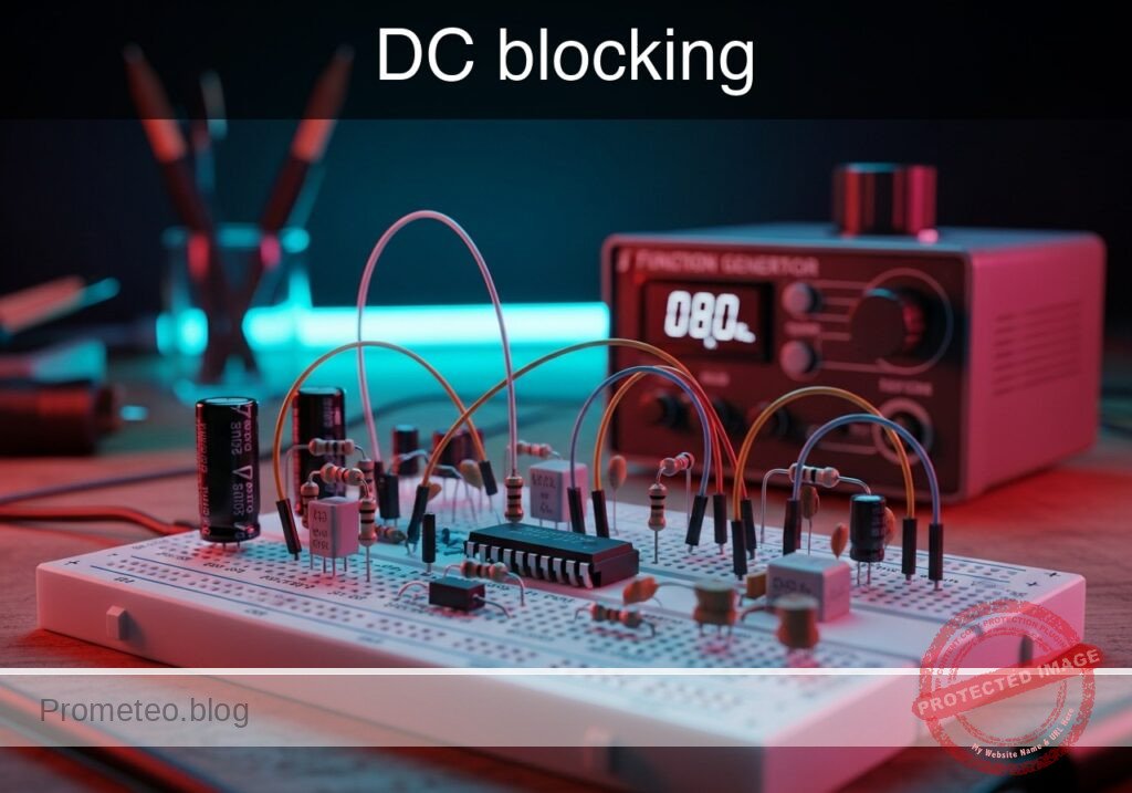
Materials
- V1: Function Generator, function: provides 1 kHz sine wave (2 Vpp) with +3 V DC offset.
- C1: 10 µF electrolytic capacitor, function: DC blocking coupling capacitor.
- R1: 10 kΩ resistor, function: output load to ground.
- Measurement Tools: Oscilloscope (DC coupling mode) and Multimeter.
Wiring guide
This circuit uses three specific nodes: VIN (source), VOUT (load), and 0 (GND).
- V1 (Source): Connect the positive terminal to node
VINand the negative/ground terminal to node0. - C1 (Capacitor): Connect the positive terminal (anode) to node
VINand the negative terminal (cathode) to nodeVOUT. - R1 (Resistor): Connect one leg to node
VOUTand the other leg to node0.
Conceptual block diagram
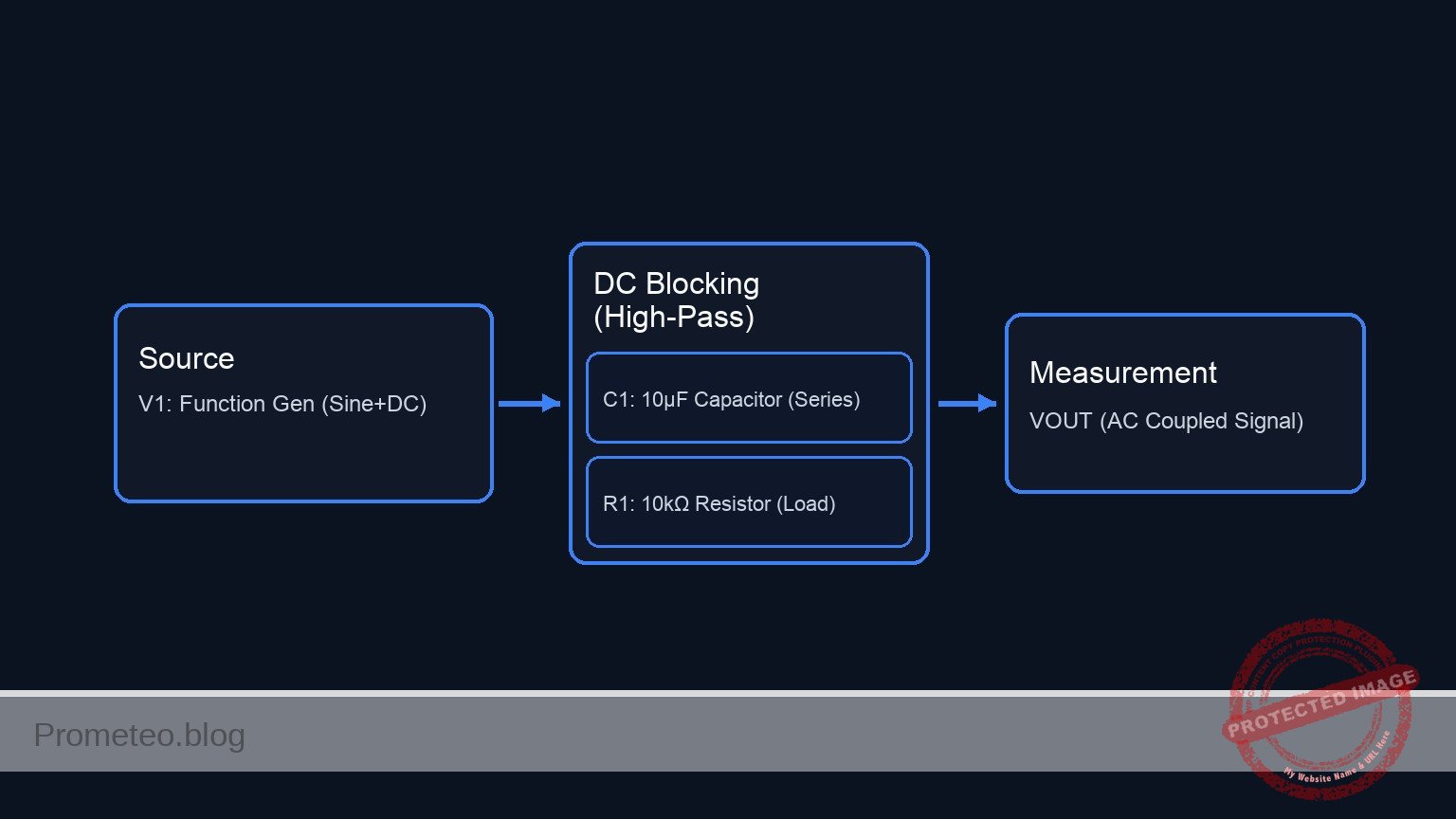
Schematic
[ INPUT SOURCE ]                 [ PROCESSING ]                   [ OUTPUT LOAD ]

    [ V1: Function Gen ]             [ C1: Capacitor ]                 [ R1: Resistor ]
    ( 1kHz Sine, 2Vpp  ) --(VIN)--> +[     10 µF     ]- --(VOUT)--> [     10 kΩ      ] --> GND
    (   +3 V DC Offset  )      |      ( Electrolytic  )       |
                              |                              |
                              v                              v
                       [ Measurement ]                [ Measurement ]
                       (Scope/Multi)                  (Scope/Multi)
Measurements and tests
To validate the circuit, ensure your oscilloscope is set to DC Coupling on the input channel. If set to AC Coupling, the scope itself will block the DC, hiding the effect of the external capacitor.
- Configure Source (V1): Set the function generator to a Sine wave, Frequency = 1 kHz, Amplitude = 2 V peak-to-peak, Offset = +3 V.
- Measure Input (VIN):
- Connect the scope probe to
VIN. - Observation: The signal should oscillate between +2 V and +4 V. The center line is at +3 V.
- DC Meter: Should read approximately +3 V.
- Connect the scope probe to
- Measure Output (VOUT):
- Connect the scope probe to
VOUT. - Observation: The signal should oscillate between -1 V and +1 V. The center line is at 0 V.
- DC Meter: Should read approximately 0 V.
- Connect the scope probe to
- Verification: Confirm that the shape and amplitude (2 Vpp) of the AC wave remain largely unchanged, but the vertical position has shifted down by 3 volts.
SPICE netlist and simulation
Reference SPICE Netlist (ngspice) — excerptFull SPICE netlist (ngspice)
* Practical case: DC blocking

* --- Components ---

* V1: Function Generator
* Specs: 1 kHz sine wave, 2 Vpp (Amplitude = 1V), +3 V DC offset
* Connection: Positive to VIN, Negative to 0 (GND)
V1 VIN 0 SIN(3 1 1k)

* C1: 10 uF electrolytic capacitor
* Function: DC blocking coupling capacitor
* Connection: Positive (VIN) to Negative (VOUT)
C1 VIN VOUT 10u

* R1: 10 kOhm resistor
* Function: Output load to ground
* Connection: VOUT to 0 (GND)
R1 VOUT 0 10k

* --- Simulation Commands ---
* ... (truncated in public view) ...
Copy this content into a .cir file and run with ngspice.
* Practical case: DC blocking

* --- Components ---

* V1: Function Generator
* Specs: 1 kHz sine wave, 2 Vpp (Amplitude = 1V), +3 V DC offset
* Connection: Positive to VIN, Negative to 0 (GND)
V1 VIN 0 SIN(3 1 1k)

* C1: 10 uF electrolytic capacitor
* Function: DC blocking coupling capacitor
* Connection: Positive (VIN) to Negative (VOUT)
C1 VIN VOUT 10u

* R1: 10 kOhm resistor
* Function: Output load to ground
* Connection: VOUT to 0 (GND)
R1 VOUT 0 10k

* --- Simulation Commands ---

* Operating point analysis
.op

* Transient analysis
* Frequency is 1kHz (Period = 1ms). Simulate 5ms to see 5 cycles.
.tran 10u 5m

* --- Output Directives ---
* Print input and output voltages for logging
.print tran V(VIN) V(VOUT)

.end
Simulation Results (Transient Analysis)

Show raw data table (508 rows)
Index   time            v(vin)          v(vout)
0	0.000000e+00	3.000000e+00	0.000000e+00
1	1.000000e-07	3.000628e+00	6.283179e-04
2	2.000000e-07	3.001257e+00	1.256635e-03
3	4.000000e-07	3.002513e+00	2.513266e-03
4	8.000000e-07	3.005027e+00	5.026506e-03
5	1.600000e-06	3.010053e+00	1.005285e-02
6	3.200000e-06	3.020105e+00	2.010452e-02
7	6.400000e-06	3.040202e+00	4.020026e-02
8	1.280000e-05	3.080338e+00	8.033296e-02
9	2.280000e-05	3.142767e+00	1.427508e-01
10	3.280000e-05	3.204633e+00	2.045991e-01
11	4.280000e-05	3.265691e+00	2.656336e-01
12	5.280000e-05	3.325700e+00	3.256134e-01
13	6.280000e-05	3.384424e+00	3.843020e-01
14	7.280000e-05	3.441631e+00	4.414676e-01
15	8.280000e-05	3.497095e+00	4.968847e-01
16	9.280000e-05	3.550597e+00	5.503345e-01
17	1.028000e-04	3.601927e+00	6.016061e-01
18	1.128000e-04	3.650880e+00	6.504972e-01
19	1.228000e-04	3.697265e+00	6.968148e-01
20	1.328000e-04	3.740898e+00	7.403761e-01
21	1.428000e-04	3.781608e+00	7.810093e-01
22	1.528000e-04	3.819232e+00	8.185538e-01
23	1.628000e-04	3.853624e+00	8.528617e-01
... (484 more rows) ...
Common mistakes and how to avoid them
- Using AC Coupling on the Oscilloscope: This is the most frequent error. It makes the input look exactly like the output because the scope blocks the DC internally. Solution: Always verify the scope channel is set to «DC Coupling».
- Reversing Capacitor Polarity: Using a polarized electrolytic capacitor backwards can cause it to leak current or fail. Solution: Ensure the positive side of C1 faces the higher DC potential (the source
VINin this case). - Load Resistance (R1) too Low: If R1 is very small, it creates a High-Pass filter with a cutoff frequency above 1 kHz, attenuating the AC signal. Solution: Ensure R1 × C1 is large enough so fcutoff = (1 / (2\pi R C)) is well below the signal frequency.
Troubleshooting
- Symptom: VOUT shows a DC voltage significantly higher than 0 V.
- Cause: The capacitor C1 is leaky or damaged (acting like a resistor).
- Fix: Replace C1 with a new capacitor.
- Symptom: No signal at VOUT (0 V AC and 0 V DC).
- Cause: Open circuit connection or defective breadboard track.
- Fix: Check continuity between C1 cathode and R1.
- Symptom: The AC signal at VOUT is much smaller than at VIN.
- Cause: The source frequency is too low for the selected C1/R1 combination (High-Pass filtering effect).
- Fix: Increase the frequency of V1 or increase the value of C1.
Possible improvements and extensions
- Frequency Sweep: Lower the frequency of V1 from 1 kHz down to 1 Hz to observe how the capacitor eventually blocks the AC signal as well (High-Pass filter demonstration).
- Variable Load: Replace R1 with a potentiometer to see how changing load impedance affects the low-frequency cutoff point.
More Practical Cases on Prometeo.blog
Find this product and/or books on this topic on Amazon
As an Amazon Associate, I earn from qualifying purchases. If you buy through this link, you help keep this project running.
Quick Quiz

Telecommunications Electronics Engineer and Computer Engineer (official degrees in Spain).

