
Level: Basic — Implement a system where a motor runs only when two buttons are pressed simultaneously.
Objective and use case
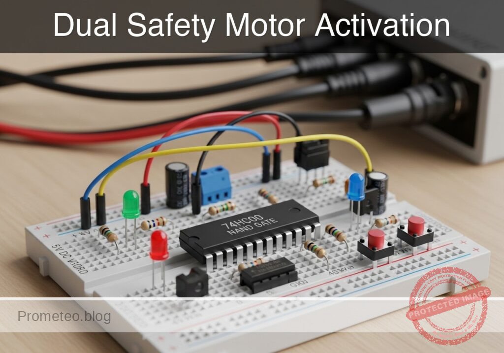
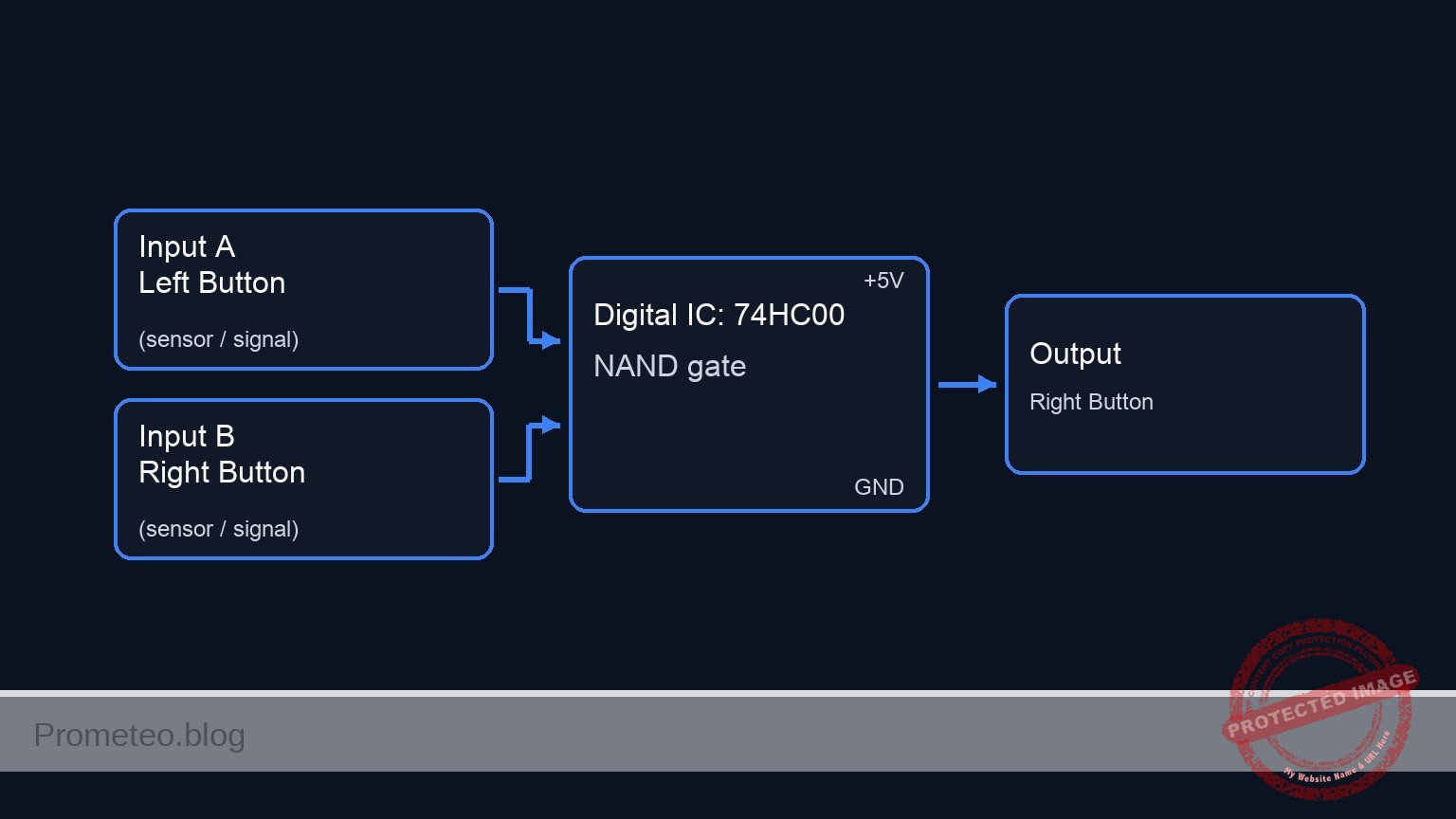
In this session, you will build a safety logic circuit using a 74HC00 (Quad 2-input NAND gate) to control a DC motor. The motor will only activate when two separate pushbuttons are engaged at the same time, mimicking a «two-hand control» safety device.
Why it is useful:
* Industrial Safety: Prevents operators from reaching into a hydraulic press or cutting machine while it is moving.
* Accident Prevention: Ensures both hands are occupied on the controls during the dangerous phase of operation.
* Logic Composition: Demonstrates how to create an AND function using universal NAND gates.
Expected outcome:
* Idle State: Logic output is LOW (0 V); Motor is OFF.
* Single Press: Logic output remains LOW (0 V); Motor remains OFF.
* Dual Press: Logic output becomes HIGH (5 V); Relay engages; Motor runs.
* Current Handling: The logic gate drives a transistor, which safely switches the high-current relay coil.
Target audience and level:
Basic electronics students and hobbyists interested in digital logic applications.
Materials
- V1: 5 V DC voltage source, function: Logic and relay coil power supply.
- V2: 12 V DC voltage source, function: Motor power supply.
- U1: 74HC00, function: Quad 2-input NAND gate IC.
- S1: Pushbutton (normally open), function: Left-hand safety switch.
- S2: Pushbutton (normally open), function: Right-hand safety switch.
- R1: 10 kΩ resistor, function: Pull-down for S1.
- R2: 10 kΩ resistor, function: Pull-down for S2.
- R3: 1 kΩ resistor, function: Base current limiting for Q1.
- Q1: 2N2222 NPN transistor, function: Relay driver.
- D1: 1N4007 diode, function: Flyback protection for relay coil.
- K1: 5 V SPDT Relay, function: High-power switching interface.
- M1: 12 V DC Motor, function: Actuator (load).
Pin-out of the IC used (74HC00)
Chip: 74HC00 (Quad 2-Input NAND Gate)
| Pin | Name | Logic Function | Connection in this case |
|---|---|---|---|
| 1 | 1 A | Input A (Gate 1) | Connected to S1 (Node BTN_L) |
| 2 | 1B | Input B (Gate 1) | Connected to S2 (Node BTN_R) |
| 3 | 1Y | Output (Gate 1) | Connected to Inputs of Gate 2 (Node NAND_INTER) |
| 4 | 2 A | Input A (Gate 2) | Connected to Node NAND_INTER |
| 5 | 2B | Input B (Gate 2) | Connected to Node NAND_INTER |
| 6 | 2Y | Output (Gate 2) | Connected to R3 (Node LOGIC_OUT) |
| 7 | GND | Ground | Connected to Node 0 |
| 14 | VCC | Power Supply | Connected to Node VCC |
Note: Pins 8 through 13 are unused and should ideally be tied to GND or VCC in a permanent installation to prevent noise, though left floating for this basic breadboard exercise.
Wiring guide
Construct the circuit following these node connections. Ensure the power supply is off while building.
Power and Inputs:
* V1 (+): Connects to node VCC.
* V1 (-) / V2 (-): Connects to node 0 (Common Ground).
* S1: Connects between VCC and node BTN_L.
* R1: Connects between node BTN_L and 0.
* S2: Connects between VCC and node BTN_R.
* R2: Connects between node BTN_R and 0.
Logic Processing (Using U1 as AND Gate):
* U1 (Pin 14): Connects to VCC.
* U1 (Pin 7): Connects to 0.
* U1 (Pin 1): Connects to node BTN_L.
* U1 (Pin 2): Connects to node BTN_R.
* U1 (Pin 3): Connects to node NAND_INTER (First stage output).
* U1 (Pin 4 & Pin 5): Both connect to node NAND_INTER (Configures Gate 2 as an inverter).
* U1 (Pin 6): Connects to node LOGIC_OUT.
Output Stage:
* R3: Connects between node LOGIC_OUT and node BASE.
* Q1 (Base): Connects to node BASE.
* Q1 (Emitter): Connects to node 0.
* Q1 (Collector): Connects to node RELAY_COIL_LO.
* K1 (Coil +): Connects to VCC.
* K1 (Coil -): Connects to node RELAY_COIL_LO.
* D1 (Anode): Connects to node RELAY_COIL_LO.
* D1 (Cathode): Connects to VCC (Parallel to coil, reverse biased).
Motor Circuit:
* V2 (+): Connects to K1 Common contact (COM).
* K1 (NO – Normally Open): Connects to node MOTOR_POS.
* M1 (+): Connects to node MOTOR_POS.
* M1 (-): Connects to node 0.
Conceptual block diagram
Schematic
+-----------------------------------------------------------------------------+
| DUAL SAFETY MOTOR ACTIVATION BLOCK DIAGRAM |
+-----------------------------------------------------------------------------+
1. INPUTS & LOGIC STAGE (5 V Domain)
(Both buttons must be pressed to activate the output)
V1(5 V)
|
+---> [ S1: Left Button ] ---+--(BTN_L)------\
| \
v \
[ R1: 10k ] +---> [ U1:A (NAND) ] --(NAND_INTER)--> [ U1:B (NOT*) ] --(LOGIC_OUT)-->
| / (Pins 1 & 2) (Pins 4 & 5) |
GND / *Wired as Inverter |
/ |
V1(5 V) / |
| / |
+---> [ S2: Right Button ] --+--(BTN_R)---/ |
| |
v |
[ R2: 10k ] |
| |
GND |
|
+-------------------------------------------------------------------------------------------------------------------+
| |
| 2. RELAY DRIVER STAGE (5 V Domain) |
| (Low-Side Transistor Switch) |
| |
| (From Logic Above) |
| | V1(5 V) |
| v | |
| [ R3: 1k ] | |
| | v |
| +----------------------------------> [ Q1: Base ] |
| : |
| (Controls Current Flow) |
| : |
| +-----------------+ |
| | |
| [ Q1: Collector ] |
| ^ |
| | |
| (Node: RELAY_COIL_LO) |
| | |
| +-----------------+-----------------+ |
| | | |
| [ K1: Relay Coil ] [ D1: Diode ] |
| (Control Side) (Protection) |
| | (Anode to Coll) |
| | (Cathode to VCC) |
| +-----------------+-----------------+ |
| ^ |
| | |
| V1(5 V) |
| |
| [ Q1: Emitter ] |
| | |
| v |
| GND |
| |
+-------------------------------------------------------------------------------------------------------------------+
| |
| 3. MOTOR OUTPUT STAGE (12 V Domain) |
| (High Power Load) |
| |
| (Magnetic Link from K1 Coil Above) |
| | |
| v |
| V2(12 V) ---------> [ K1: Switch (COM to NO) ] --(MOTOR_POS)--> [ M1: 12 V Motor ] ----> GND |
| |
+-------------------------------------------------------------------------------------------------------------------+
Truth table
We are using two NAND gates. The first combines the inputs; the second inverts the result to create an AND function.
| S1 (Left) | S2 (Right) | U1 Pin 3 (1Y) | U1 Pin 6 (2Y) | Motor State |
|---|---|---|---|---|
| 0 (OFF) | 0 (OFF) | 1 (High) | 0 (Low) | STOP |
| 0 (OFF) | 1 (ON) | 1 (High) | 0 (Low) | STOP |
| 1 (ON) | 0 (OFF) | 1 (High) | 0 (Low) | STOP |
| 1 (ON) | 1 (ON) | 0 (Low) | 1 (High) | RUN |
Measurements and tests
- Idle Check: Power on V1. Do not press any buttons. Measure the voltage at
LOGIC_OUT(Pin 6). It should be ~0 V. The motor should be stopped. - Input Validation: Press S1 only. Measure voltage at Pin 1. It should be 5 V. Pin 2 should be 0 V. Output at Pin 6 must remain 0 V.
- Active Test: Press and hold both S1 and S2 simultaneously.
- Listen for the «click» of the relay K1.
- Observe M1 spinning.
- Measure the voltage at
LOGIC_OUT; it should be close to 5 V.
- Release Test: Release just one button. The motor must stop immediately.
SPICE netlist and simulation
Reference SPICE Netlist (ngspice) — excerptFull SPICE netlist (ngspice)
* Practical case: Logic AND gate controlling a relay and motor

* ==============================================================================
* COMPONENT MODELS
* ==============================================================================
* Generic NPN Transistor Model (2N2222)
.model 2N2222MOD NPN(Is=14.34f Xti=3 Eg=1.11 Vaf=74.03 Bf=255.9 Ne=1.307 Ise=14.34f Ikf=.2847 Xtb=1.5 Br=6.092 Nc=2 Isc=0 Ikr=0 Rc=1 Cjc=7.306p Mjc=.3416 Vjc=.75 Fc=.5 Cje=22.01p Mje=.377 Vje=.75 Tr=46.91n Tf=411.1p Itf=.6 Vtf=1.7 Xtf=3 Rb=10)

* Generic Diode Model (1N4007)
.model D1N4007 D(IS=7.02767n RS=0.0341512 N=1.80803 EG=1.11 XTI=3 BV=1000 IBV=10m CJO=10p VJ=0.7 M=0.5 FC=0.5 TT=100n)

* Ideal Switch Model for Buttons and Relay Contact
* Vt=2.5V (Logic Threshold), Ron=0.1 Ohm, Roff=10 MegOhm
.model SW_IDEAL SW(Vt=2.5 Vh=0.1 Ron=0.1 Roff=10Meg)

* ==============================================================================
* POWER SUPPLIES
* ==============================================================================
* V1: 5V DC Supply for Logic and Relay Coil
V1 VCC 0 DC 5
* ... (truncated in public view) ...
Copy this content into a .cir file and run with ngspice.
* Practical case: Logic AND gate controlling a relay and motor

* ==============================================================================
* COMPONENT MODELS
* ==============================================================================
* Generic NPN Transistor Model (2N2222)
.model 2N2222MOD NPN(Is=14.34f Xti=3 Eg=1.11 Vaf=74.03 Bf=255.9 Ne=1.307 Ise=14.34f Ikf=.2847 Xtb=1.5 Br=6.092 Nc=2 Isc=0 Ikr=0 Rc=1 Cjc=7.306p Mjc=.3416 Vjc=.75 Fc=.5 Cje=22.01p Mje=.377 Vje=.75 Tr=46.91n Tf=411.1p Itf=.6 Vtf=1.7 Xtf=3 Rb=10)

* Generic Diode Model (1N4007)
.model D1N4007 D(IS=7.02767n RS=0.0341512 N=1.80803 EG=1.11 XTI=3 BV=1000 IBV=10m CJO=10p VJ=0.7 M=0.5 FC=0.5 TT=100n)

* Ideal Switch Model for Buttons and Relay Contact
* Vt=2.5V (Logic Threshold), Ron=0.1 Ohm, Roff=10 MegOhm
.model SW_IDEAL SW(Vt=2.5 Vh=0.1 Ron=0.1 Roff=10Meg)

* ==============================================================================
* POWER SUPPLIES
* ==============================================================================
* V1: 5V DC Supply for Logic and Relay Coil
V1 VCC 0 DC 5

* V2: 12V DC Supply for Motor
V2 V_MOTOR_RAIL 0 DC 12

* ==============================================================================
* INPUT STAGE (Safety Switches)
* ==============================================================================
* Simulation of User Pressing Buttons:
* We use Pulse sources (V_ACT_...) to control ideal switches (S1, S2).
* This preserves the Pull-down resistor topology.

* S1: Left Safety Switch (Pushbutton NO)
* Connects VCC to BTN_L when pressed.
* Pulse Pattern: Period 120us, Pulse 50us (Tests asynchronous press)
V_ACT_L ACT_L 0 PULSE(0 5 10u 1u 1u 50u 120u)
S1 VCC BTN_L ACT_L 0 SW_IDEAL
R1 BTN_L 0 10k

* S2: Right Safety Switch (Pushbutton NO)
* Connects VCC to BTN_R when pressed.
* Pulse Pattern: Period 100us, Pulse 50us
V_ACT_R ACT_R 0 PULSE(0 5 20u 1u 1u 50u 100u)
S2 VCC BTN_R ACT_R 0 SW_IDEAL
R2 BTN_R 0 10k

* ==============================================================================
* LOGIC STAGE (U1: 74HC00 Quad NAND)
* ==============================================================================
* Implementing logic using Behavioral Voltage Sources (B-Sources) with continuous
* sigmoid functions for convergence robustness.
* Logic High = 5V, Logic Low = 0V. Threshold ~ 2.5V.

* U1 Gate 1: Inputs BTN_L (Pin 1), BTN_R (Pin 2) -> Output NAND_INTER (Pin 3)
* Function: NAND(BTN_L, BTN_R)
B_U1_G1 NAND_INTER 0 V=5 * (1 - ( (1/(1+exp(-20*(V(BTN_L)-2.5)))) * (1/(1+exp(-20*(V(BTN_R)-2.5)))) ))

* U1 Gate 2: Inputs NAND_INTER (Pin 4, 5) -> Output LOGIC_OUT (Pin 6)
* Function: NAND(NAND_INTER, NAND_INTER) = NOT(NAND_INTER)
* Combined Function: AND(BTN_L, BTN_R)
B_U1_G2 LOGIC_OUT 0 V=5 * (1 - ( (1/(1+exp(-20*(V(NAND_INTER)-2.5)))) * (1/(1+exp(-20*(V(NAND_INTER)-2.5)))) ))

* ==============================================================================
* OUTPUT DRIVER STAGE
* ==============================================================================
* R3: Base current limiting
R3 LOGIC_OUT BASE 1k

* Q1: 2N2222 Relay Driver
* Emitter to GND, Collector to RELAY_COIL_LO
Q1 RELAY_COIL_LO BASE 0 2N2222MOD

* ==============================================================================
* RELAY STAGE (K1)
* ==============================================================================
* Relay Coil Configuration:
* Connected between VCC and RELAY_COIL_LO.
* Modeled as Inductor + Series Resistor.
L_K1 VCC K1_NODE 10m
R_K1 K1_NODE RELAY_COIL_LO 100

* D1: Flyback Diode (1N4007)
* Anode to RELAY_COIL_LO, Cathode to VCC (Reverse biased)
D1 RELAY_COIL_LO VCC D1N4007

* Relay Contact (Switch):
* Logic: Switch closes when Coil is energized.
* Coil is energized when Q1 is ON (RELAY_COIL_LO is Low).
* Control Voltage = V(VCC) - V(RELAY_COIL_LO).
* If Q1 ON: 5V - 0.2V = 4.8V (> 2.5V Threshold) -> Switch CLOSED.
* If Q1 OFF: 5V - 5V = 0V (< 2.5V Threshold) -> Switch OPEN.
B_K1_CTRL K1_CTRL 0 V = V(VCC) - V(RELAY_COIL_LO)
S_K1 V_MOTOR_RAIL MOTOR_POS K1_CTRL 0 SW_IDEAL

* ==============================================================================
* LOAD (Motor M1)
* ==============================================================================
* M1: 12V DC Motor connected between MOTOR_POS and 0
* Modeled as Resistor + Inductor
R_M1 MOTOR_POS M1_INT 20
L_M1 M1_INT 0 5m

* ==============================================================================
* ANALYSIS COMMANDS
* ==============================================================================
.op
* Transient analysis: 1us step, 500us total time
.tran 1u 500u

* Print results for batch processing
* Inputs: BTN_L, BTN_R
* Output: MOTOR_POS (Load Voltage)
* Debug: LOGIC_OUT, RELAY_COIL_LO
.print tran V(BTN_L) V(BTN_R) V(MOTOR_POS) V(LOGIC_OUT) V(RELAY_COIL_LO) I(L_M1)

.end
Simulation Results (Transient Analysis)

Show raw data table (1202 rows)
Index   time            v(btn_l)        v(btn_r)        v(motor_pos)    v(logic_out)    v(relay_coil_lo l_m1#branch
0	0.000000e+00	4.995005e-03	4.995005e-03	2.399995e-05	-6.01853e-36	5.000000e+00	1.199998e-06
1	1.000000e-08	4.995005e-03	4.995005e-03	2.399995e-05	-6.01853e-36	5.000000e+00	1.199998e-06
2	2.000000e-08	4.995005e-03	4.995005e-03	2.399995e-05	-6.01853e-36	5.000000e+00	1.199998e-06
3	4.000000e-08	4.995005e-03	4.995005e-03	2.399995e-05	-6.01853e-36	5.000000e+00	1.199998e-06
4	8.000000e-08	4.995005e-03	4.995005e-03	2.399995e-05	-6.01853e-36	5.000000e+00	1.199998e-06
5	1.600000e-07	4.995005e-03	4.995005e-03	2.399995e-05	-6.01853e-36	5.000000e+00	1.199998e-06
6	3.200000e-07	4.995005e-03	4.995005e-03	2.399995e-05	-6.01853e-36	5.000000e+00	1.199998e-06
7	6.400000e-07	4.995005e-03	4.995005e-03	2.399995e-05	-6.01853e-36	5.000000e+00	1.199998e-06
8	1.280000e-06	4.995005e-03	4.995005e-03	2.399995e-05	-6.01853e-36	5.000000e+00	1.199998e-06
9	2.280000e-06	4.995005e-03	4.995005e-03	2.399995e-05	-6.01853e-36	5.000000e+00	1.199998e-06
10	3.280000e-06	4.995005e-03	4.995005e-03	2.399995e-05	-6.01853e-36	5.000000e+00	1.199998e-06
11	4.280000e-06	4.995005e-03	4.995005e-03	2.399995e-05	-6.01853e-36	5.000000e+00	1.199998e-06
12	5.280000e-06	4.995005e-03	4.995005e-03	2.399995e-05	-6.01853e-36	5.000000e+00	1.199998e-06
13	6.280000e-06	4.995005e-03	4.995005e-03	2.399995e-05	-6.01853e-36	5.000000e+00	1.199998e-06
14	7.280000e-06	4.995005e-03	4.995005e-03	2.399995e-05	-6.01853e-36	5.000000e+00	1.199998e-06
15	8.280000e-06	4.995005e-03	4.995005e-03	2.399995e-05	-6.01853e-36	5.000000e+00	1.199998e-06
16	9.280000e-06	4.995005e-03	4.995005e-03	2.399995e-05	-6.01853e-36	5.000000e+00	1.199998e-06
17	1.000000e-05	4.995005e-03	4.995005e-03	2.399995e-05	-6.01853e-36	5.000000e+00	1.199998e-06
18	1.010000e-05	4.995005e-03	4.995005e-03	2.399995e-05	-6.01853e-36	5.000000e+00	1.199998e-06
19	1.027500e-05	4.995005e-03	4.995005e-03	2.399995e-05	-6.01853e-36	5.000000e+00	1.199998e-06
20	1.032344e-05	4.995005e-03	4.995005e-03	2.399995e-05	-6.01853e-36	5.000000e+00	1.199998e-06
21	1.040820e-05	4.995005e-03	4.995005e-03	2.399995e-05	-6.01853e-36	5.000000e+00	1.199998e-06
22	1.043167e-05	4.995005e-03	4.995005e-03	2.399995e-05	-6.01853e-36	5.000000e+00	1.199998e-06
23	1.047272e-05	4.995005e-03	4.995005e-03	2.399995e-05	-6.01853e-36	5.000000e+00	1.199998e-06
... (1178 more rows) ...
Common mistakes and how to avoid them
- Floating Inputs: Forgetting R1 or R2 causes the NAND gate inputs to float, often reading as «High» due to noise. Solution: Ensure pull-down resistors are firmly connected to Ground.
- Missing Flyback Diode: Omitting D1 creates voltage spikes when the relay turns off, which can destroy Q1 or reset the logic chip. Solution: Always place a diode across the relay coil (Cathode to positive).
- Direct Drive: Attempting to drive the motor or relay directly from the 74HC00 output pin. Solution: Always use a transistor (Q1) to amplify the current for inductive loads like relays.
Troubleshooting
- Motor runs immediately upon power-up: Check if S1 or S2 are wired as Normally Closed instead of Normally Open, or if the transistor Q1 is shorted.
- Relay clicks but motor doesn’t run: Check the V2 power supply and the connections on the relay contacts (COM and NO).
- Logic works but gets hot: Check if VCC (Pin 14) and GND (Pin 7) are reversed. Disconnect power immediately.
- Erratic behavior: Add a 100 nF decoupling capacitor between Pin 14 and Pin 7 of the IC, close to the chip.
Possible improvements and extensions
- Emergency Stop: Add a Normally Closed (NC) latching button in series with the relay coil or the base resistor R3 to cut power instantly regardless of logic state.
- Visual Feedback: Add a green LED (with a 330 Ω resistor) connected to node
LOGIC_OUTto indicate when the safety condition is met, even if the motor power (V2) is off.
More Practical Cases on Prometeo.blog
Find this product and/or books on this topic on Amazon
As an Amazon Associate, I earn from qualifying purchases. If you buy through this link, you help keep this project running.
Quick Quiz

Telecommunications Electronics Engineer and Computer Engineer (official degrees in Spain).

