
Level: Basic. Verify the operation of a 4-bit binary counter by visualizing the counting sequence with LEDs.
Objective and use case
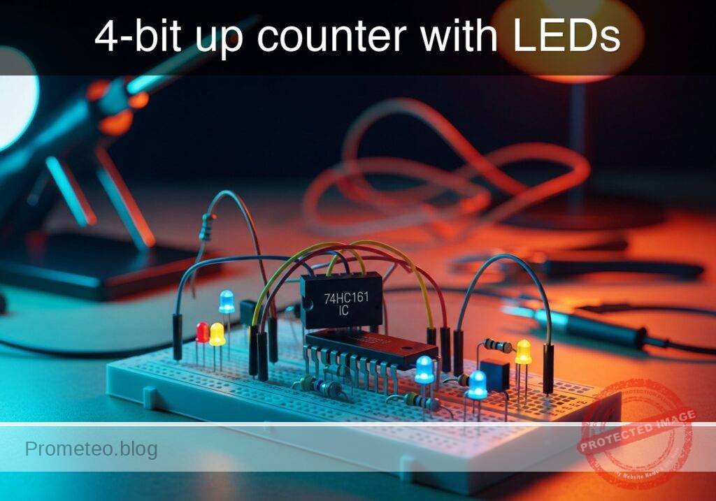
In this practical case, you will build a synchronous digital circuit using the 74HC161 integrated circuit to count clock pulses in binary from 0 (0000) to 15 (1111). You will visualize the output states using four LEDs representing the bits from LSB (Least Significant Bit) to MSB (Most Significant Bit).
Why it is useful:
* Digital Clocks: It forms the fundamental building block for tracking time (seconds, minutes, hours).
* Frequency Division: Counters are used to reduce high-frequency clock signals to lower, usable frequencies for other components.
* Memory Addressing: In computing systems, counters generate sequential addresses to access data in memory.
* Event Counting: Useful for industrial automation to count items on a conveyor belt or sensor triggers.
* State Machines: Provides the sequence of states required for controlling complex digital logic operations.
Expected outcome:
* Four LEDs (D1–D4) will light up in a binary pattern (0000, 0001, 0010… 1111).
* The sequence repeats every 16 clock pulses.
* Activating the reset switch forces all LEDs to turn OFF immediately.
* Logic High output voltage approx. 5 V; Logic Low approx. 0 V.
Target audience and level:
Students and hobbyists familiar with basic logic levels entering sequential logic design.
Materials
- U1: 74HC161, function: 4-bit synchronous binary counter IC
- V1: 5 V DC supply, function: main power source
- V2: Pulse voltage source (0 V to 5 V), function: Clock signal (1 Hz for visualization)
- R1: 330 Ω resistor, function: current limiting for LED Q0
- R2: 330 Ω resistor, function: current limiting for LED Q1
- R3: 330 Ω resistor, function: current limiting for LED Q2
- R4: 330 Ω resistor, function: current limiting for LED Q3
- R5: 10 kΩ resistor, function: pull-up for Master Reset
- D1: Red LED, function: Indicator for Q0 (LSB)
- D2: Red LED, function: Indicator for Q1
- D3: Red LED, function: Indicator for Q2
- D4: Red LED, function: Indicator for Q3 (MSB)
- S1: Momentary push button (normally open), function: Reset trigger
Pin-out of the IC used
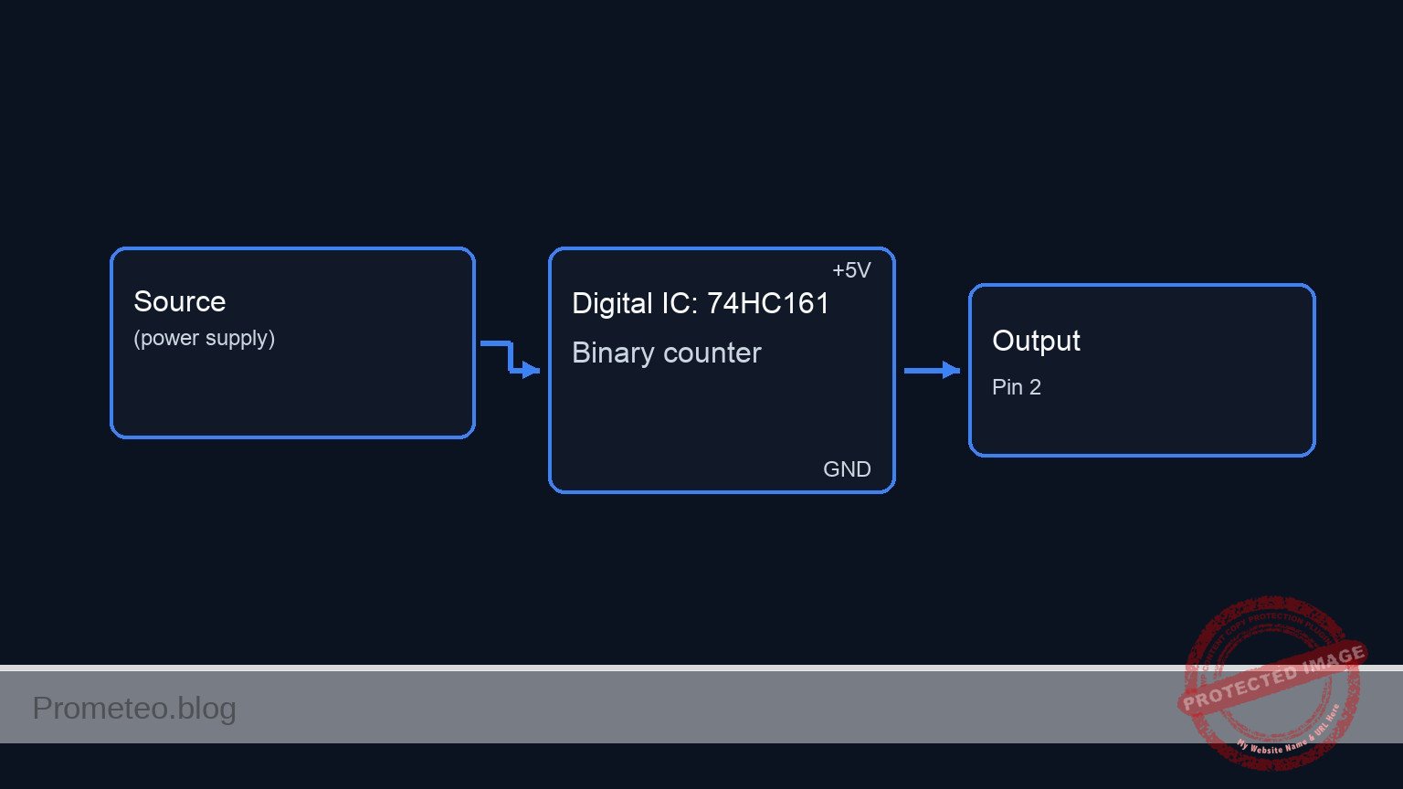
Selected Chip: 74HC161 (4-bit Synchronous Binary Counter, Asynchronous Reset)
| Pin | Name | Logic function | Connection in this case |
|---|---|---|---|
| 1 | \overlineMR | Master Reset (Active Low) | Connected to Reset node (S1/R5) |
| 2 | CP | Clock Pulse (Rising Edge) | Connected to V2 (Clock Source) |
| 7 | CEP | Count Enable Parallel | Connected to VCC (Always Enabled) |
| 8 | GND | Ground | Connected to 0 (GND) |
| 9 | \overlinePE | Parallel Enable (Load) | Connected to VCC (Disabled) |
| 10 | CET | Count Enable Trickle | Connected to VCC (Always Enabled) |
| 11 | Q3 | Output Bit 3 (MSB) | Connected to D4 via R4 |
| 12 | Q2 | Output Bit 2 | Connected to D3 via R3 |
| 13 | Q1 | Output Bit 1 | Connected to D2 via R2 |
| 14 | Q0 | Output Bit 0 (LSB) | Connected to D1 via R1 |
| 16 | VCC | Power Supply (+5 V) | Connected to VCC |
Note: Pins 3, 4, 5, 6 (Parallel Data Inputs) and 15 (Ripple Carry Output) are not used in this basic counting configuration and inputs can be tied to ground if preferred, though usually irrelevant when Load is disabled.
Wiring guide
Construct the circuit following these explicit node connections:
-
Power Nodes:
- Connect
V1positive terminal to nodeVCC. - Connect
V1negative terminal to node0(GND). - Connect
U1pin 16 toVCC. - Connect
U1pin 8 to0.
- Connect
-
Control Inputs:
- Connect
V2(Clock Source) positive to nodeCLK. ConnectV2negative to0. - Connect
U1pin 2 to nodeCLK. - Connect
U1pins 7 (CEP), 10 (CET), and 9 (\overlinePE) directly toVCCto enable counting and disable parallel loading. - Reset Circuit: Connect
R5betweenVCCand nodeRESET_N. ConnectS1between nodeRESET_Nand0. ConnectU1pin 1 toRESET_N.
- Connect
-
Outputs (LED Indicators):
- Bit 0 (LSB): Connect
U1pin 14 to nodeQ0. ConnectR1betweenQ0and nodeLED_A1. ConnectD1anode toLED_A1and cathode to0. - Bit 1: Connect
U1pin 13 to nodeQ1. ConnectR2betweenQ1and nodeLED_A2. ConnectD2anode toLED_A2and cathode to0. - Bit 2: Connect
U1pin 12 to nodeQ2. ConnectR3betweenQ2and nodeLED_A3. ConnectD3anode toLED_A3and cathode to0. - Bit 3 (MSB): Connect
U1pin 11 to nodeQ3. ConnectR4betweenQ3and nodeLED_A4. ConnectD4anode toLED_A4and cathode to0.
- Bit 0 (LSB): Connect
Conceptual block diagram
Schematic
+-------------------------------------------------------------------------------------------------------+
|                                  PRACTICAL CASE: 4-BIT UP COUNTER                                     |
+-------------------------------------------------------------------------------------------------------+

      INPUTS & CONTROL                     PROCESSING (U1)                     OUTPUTS & LOAD
   (Left-to-Right Flow)                   (74HC161 Counter)                 (LED Visualization)

                                     +-------------------------+
                                     |                         |
[ V2: Clock Source ] --(CLK 1Hz)---> | [Pin 2] CP              |
                                     |                         |
                                     |                         |          (Bit 0 - LSB)
[ Reset Logic ]                      |             [Pin 14] Q0 | --(Q0)--> [ R1: 330 ] --> [ D1: Red ] --> GND
(VCC->R5->Node->S1->GND) --(RST_N)-> | [Pin 1] ~MR             |
                                     |                         |
                                     |                         |          (Bit 1)
                                     |             [Pin 13] Q1 | --(Q1)--> [ R2: 330 ] --> [ D2: Red ] --> GND
[ VCC: 5 V Source ] --(Enable High)-> | [Pin 7]  CEP            |
                   --(Enable High)-> | [Pin 10] CET            |
                   --(Disable Load)> | [Pin 9]  ~PE            |          (Bit 2)
                                     |             [Pin 12] Q2 | --(Q2)--> [ R3: 330 ] --> [ D3: Red ] --> GND
                                     |                         |
                                     |                         |
                                     |                         |          (Bit 3 - MSB)
                                     |             [Pin 11] Q3 | --(Q3)--> [ R4: 330 ] --> [ D4: Red ] --> GND
                                     |                         |
                                     +-------------------------+
                                            |           |
                                         [Pin 16]    [Pin 8]
                                            |           |
                                           VCC         GND
Measurements and tests
- Supply Check: Before connecting the IC, measure voltage between
VCCand0to ensure it is stable at 5 V. - Clock Verification: Set
V2to a low frequency (e.g., 1 Hz). Verify the signal at nodeCLKoscillates between 0 V and 5 V. - Sequence Observation: Power on the circuit. Observe
D1throughD4. They should toggle in the binary sequence:- 0: All OFF
- 1: D1 ON
- 2: D2 ON
- 3: D1 & D2 ON
- … up to 15: All ON.
- Reset Test: While the counter is running, press
S1. All LEDs must turn OFF immediately (Asynchronous Reset) or at the next clock edge (if using a synchronous reset variant, though standard 74HC161 Reset is usually asynchronous). - Logic Levels: Use a multimeter to measure node
Q3when D4 is lit. It should read close to 5 V (Logic High).
SPICE netlist and simulation
Reference SPICE Netlist (ngspice) — excerptFull SPICE netlist (ngspice)
* Practical case: 4-bit up counter with LEDs (74HC161)
* NGSPICE Netlist
* Requires XSPICE extensions

.width out=256

* --- Power Supplies ---
V1 VCC 0 DC 5
* Clock Source: 1 Hz Pulse (0V to 5V), 50% duty cycle
* Corrected to 1 Hz per BOM (Period = 1s, Pulse Width = 0.5s)
V2 CLK 0 PULSE(0 5 0 1u 1u 0.5 1)

* --- Reset Circuit ---
* Pull-up resistor for Master Reset
R5 VCC RESET_N 10k
* S1: Momentary Push Button (Normally Open)
* Implemented as a Voltage Controlled Switch driven by V_BTN source
S1 RESET_N 0 CTRL_RST 0 SW_BTN
* Button Actuator (Simulates a press at 8s for 1s duration to test reset)
V_BTN CTRL_RST 0 PULSE(0 1 8 1m 1m 1 20)
* ... (truncated in public view) ...
Copy this content into a .cir file and run with ngspice.
* Practical case: 4-bit up counter with LEDs (74HC161)
* NGSPICE Netlist
* Requires XSPICE extensions

.width out=256

* --- Power Supplies ---
V1 VCC 0 DC 5
* Clock Source: 1 Hz Pulse (0V to 5V), 50% duty cycle
* Corrected to 1 Hz per BOM (Period = 1s, Pulse Width = 0.5s)
V2 CLK 0 PULSE(0 5 0 1u 1u 0.5 1)

* --- Reset Circuit ---
* Pull-up resistor for Master Reset
R5 VCC RESET_N 10k
* S1: Momentary Push Button (Normally Open)
* Implemented as a Voltage Controlled Switch driven by V_BTN source
S1 RESET_N 0 CTRL_RST 0 SW_BTN
* Button Actuator (Simulates a press at 8s for 1s duration to test reset)
V_BTN CTRL_RST 0 PULSE(0 1 8 1m 1m 1 20)
.model SW_BTN sw(vt=0.5 ron=1 roff=10Meg)

* --- 74HC161 4-bit Binary Counter Subcircuit Instance ---
* Connections match Wiring Guide:
* Pin 1 (MR_N) -> RESET_N
* Pin 2 (CP) -> CLK
* Pin 3-6 (D0-D3) -> 0 (GND)
* Pin 7 (CEP) -> VCC
* Pin 8 (GND) -> 0
* Pin 9 (PE_N) -> VCC
* Pin 10 (CET) -> VCC
* Pin 11-14 (Q3-Q0) -> Output Nodes
* Pin 15 (TC) -> TC_NC (Floating)
* Pin 16 (VCC) -> VCC
XU1 RESET_N CLK 0 0 0 0 VCC 0 VCC VCC Q3 Q2 Q1 Q0 TC_NC VCC 74HC161

* --- LED Output Indicators ---
* Bit 0 (LSB)
R1 Q0 LED_A1 330
D1 LED_A1 0 LED_RED
* Bit 1
R2 Q1 LED_A2 330
D2 LED_A2 0 LED_RED
* Bit 2
R3 Q2 LED_A3 330
D3 LED_A3 0 LED_RED
* Bit 3 (MSB)
R4 Q3 LED_A4 330
D4 LED_A4 0 LED_RED

* --- Models ---
.model LED_RED D(Is=1e-14 Rs=5 N=2)

* --- Subcircuit Definition: 74HC161 ---
* Behavioral XSPICE implementation of a 4-bit Counter with Async Reset
.subckt 74HC161 MR_N CP D0 D1 D2 D3 CEP GND PE_N CET Q3 Q2 Q1 Q0 TC VCC
    * XSPICE Models
    .model adc_in adc_bridge(in_low=2.0 in_high=3.0)
    .model dac_out dac_bridge(out_low=0.0 out_high=5.0)
    .model dff_mod d_dff(rise_delay=10n fall_delay=10n)
    .model inv_mod d_inverter(rise_delay=5n fall_delay=5n)

    * Input Bridges (Analog to Digital)
    A_IN [MR_N CP] [mr_dig cp_dig] adc_in

    * Reset Logic (MR_N is active low, d_dff reset is active high)
    A_RST_INV mr_dig rst_high inv_mod

    * Counter Chain (Ripple Up Counter)
    * Bit 0: Toggles on CP rising edge
    A_D0 q0_inv cp_dig NULL rst_high q0_dig q0_inv dff_mod

    * Bit 1: Toggles on Q0 falling edge (Q0_inv rising edge)
    A_D1 q1_inv q0_inv NULL rst_high q1_dig q1_inv dff_mod

    * Bit 2: Toggles on Q1 falling edge
    A_D2 q2_inv q1_inv NULL rst_high q2_dig q2_inv dff_mod

    * Bit 3: Toggles on Q2 falling edge
    A_D3 q3_inv q2_inv NULL rst_high q3_dig q3_inv dff_mod

    * Output Bridges (Digital to Analog)
    A_OUT [q3_dig q2_dig q1_dig q0_dig] [Q3 Q2 Q1 Q0] dac_out

    * Terminal Count (Unused/Dummy pull-down)
    R_TC TC 0 100k
.ends

* --- Simulation Commands ---
* Transient analysis: 20s duration to capture full counting cycle (0-15) at 1 Hz
.op
.tran 10m 20s

* Print critical signals (Inputs first)
.print tran V(CLK) V(RESET_N) V(Q0) V(Q1) V(Q2) V(Q3)

.end
Simulation Results (Transient Analysis)

Show raw data table (3020 rows)
Index   time            v(clk)          v(reset_n)      v(q0)           v(q1)           v(q2)           v(q3)
0	0.000000e+00	0.000000e+00	4.995005e+00	0.000000e+00	0.000000e+00	0.000000e+00	0.000000e+00
1	1.000000e-08	5.000000e-02	4.995005e+00	0.000000e+00	0.000000e+00	0.000000e+00	0.000000e+00
2	2.000000e-08	1.000000e-01	4.995005e+00	0.000000e+00	0.000000e+00	0.000000e+00	0.000000e+00
3	4.000000e-08	2.000000e-01	4.995005e+00	0.000000e+00	0.000000e+00	0.000000e+00	0.000000e+00
4	8.000000e-08	4.000000e-01	4.995005e+00	0.000000e+00	0.000000e+00	0.000000e+00	0.000000e+00
5	1.600000e-07	8.000000e-01	4.995005e+00	0.000000e+00	0.000000e+00	0.000000e+00	0.000000e+00
6	3.200000e-07	1.600000e+00	4.995005e+00	0.000000e+00	0.000000e+00	0.000000e+00	0.000000e+00
7	6.400000e-07	3.200000e+00	4.995005e+00	0.000000e+00	0.000000e+00	0.000000e+00	0.000000e+00
8	6.520000e-07	3.260000e+00	4.995005e+00	0.000000e+00	0.000000e+00	0.000000e+00	0.000000e+00
9	6.760000e-07	3.380000e+00	4.995005e+00	5.000000e+00	0.000000e+00	0.000000e+00	0.000000e+00
10	7.240000e-07	3.620000e+00	4.995005e+00	5.000000e+00	0.000000e+00	0.000000e+00	0.000000e+00
11	8.200000e-07	4.100000e+00	4.995005e+00	5.000000e+00	0.000000e+00	0.000000e+00	0.000000e+00
12	1.000000e-06	5.000000e+00	4.995005e+00	5.000000e+00	0.000000e+00	0.000000e+00	0.000000e+00
13	1.019200e-06	5.000000e+00	4.995005e+00	5.000000e+00	0.000000e+00	0.000000e+00	0.000000e+00
14	1.057600e-06	5.000000e+00	4.995005e+00	5.000000e+00	0.000000e+00	0.000000e+00	0.000000e+00
15	1.134400e-06	5.000000e+00	4.995005e+00	5.000000e+00	0.000000e+00	0.000000e+00	0.000000e+00
16	1.288000e-06	5.000000e+00	4.995005e+00	5.000000e+00	0.000000e+00	0.000000e+00	0.000000e+00
17	1.595200e-06	5.000000e+00	4.995005e+00	5.000000e+00	0.000000e+00	0.000000e+00	0.000000e+00
18	2.209600e-06	5.000000e+00	4.995005e+00	5.000000e+00	0.000000e+00	0.000000e+00	0.000000e+00
19	3.438400e-06	5.000000e+00	4.995005e+00	5.000000e+00	0.000000e+00	0.000000e+00	0.000000e+00
20	5.896000e-06	5.000000e+00	4.995005e+00	5.000000e+00	0.000000e+00	0.000000e+00	0.000000e+00
21	1.081120e-05	5.000000e+00	4.995005e+00	5.000000e+00	0.000000e+00	0.000000e+00	0.000000e+00
22	2.064160e-05	5.000000e+00	4.995005e+00	5.000000e+00	0.000000e+00	0.000000e+00	0.000000e+00
23	4.030240e-05	5.000000e+00	4.995005e+00	5.000000e+00	0.000000e+00	0.000000e+00	0.000000e+00
... (2996 more rows) ...
Common mistakes and how to avoid them
- Leaving Enable pins floating: The 74HC series has high impedance inputs. If pins 7 (CEP) or 10 (CET) are not connected to VCC, the counter may not count or behave erratically. Always tie unused control inputs to a defined logic level.
- Clock frequency too high: If
V2is set to 1 kHz or higher, all LEDs will appear to be dimly lit continuously due to persistence of vision. Keep the clock below 5 Hz for visual debugging. - Floating Parallel Load pin: If pin 9 (\overlinePE) is left floating or low, the chip might constantly try to load data from inputs P0-P3 instead of counting. Ensure pin 9 is tied to VCC.
Troubleshooting
- LEDs never turn on: Check power supply connections to pins 16 and 8. Ensure LEDs are inserted with the correct polarity (anode to resistor/IC, cathode to ground).
- Counter stays at zero: Verify that the Reset pin (1) is High (5 V). If
S1is stuck or the pull-upR5is missing, the chip remains in Reset state. Also, check that Enable pins (7, 10) are High. - Counter skips numbers: This is often due to «switch bounce» if you are using a mechanical switch as a manual clock. Use a clean square wave generator or a debounce circuit (capacitor + resistor) for the clock input.
- Random sequence: Check if the Parallel Enable (\overlinePE) pin is accidentally Low or floating. It must be High.
Possible improvements and extensions
- 8-bit Counter: Cascade a second 74HC161 by connecting the Carry Output (pin 15) of the first counter to the Enable Trickle (pin 10) of the second counter. This allows counting up to 255.
- Manual Clock: Replace the frequency generator
V2with a 555 timer circuit in astable mode or a debounced push-button to advance the count manually.
More Practical Cases on Prometeo.blog
Find this product and/or books on this topic on Amazon
As an Amazon Associate, I earn from qualifying purchases. If you buy through this link, you help keep this project running.
Quick Quiz

Telecommunications Electronics Engineer and Computer Engineer (official degrees in Spain).

