
Level: Basic – Design a circuit that counts from 0 to 9 and resets automatically using combinational logic.
Objective and use case
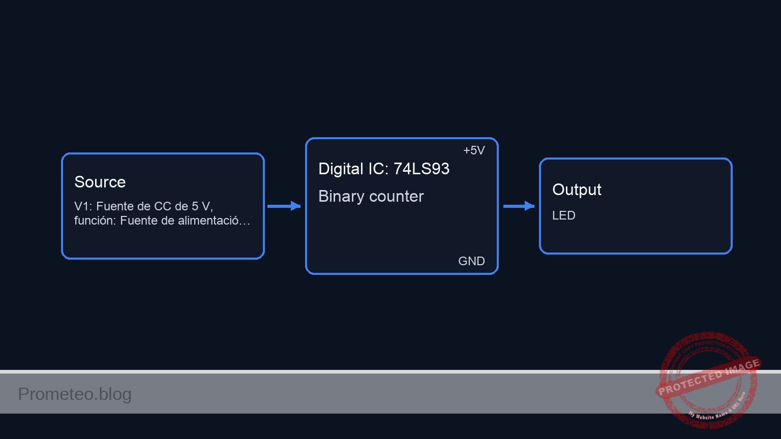
In this practical case, you will build a 4-bit asynchronous counter using the 74LS93 IC that counts from 0 to 9 (binary) and automatically resets when it reaches the decimal value 10 (binary 1010). We will use an external AND gate to detect the reset condition.
Why it is useful:
* Digital Clocks: Serves as the fundamental unit for counting seconds or minutes (0-9).
* Frequency Division: Divides an input frequency by 10 to reduce clock speeds in digital systems.
* Industrial Automation: Counts items on a conveyor belt in batches of 10.
* User Interfaces: Cycles through menu options or presets in a loop.
Expected outcome:
* Four LEDs displaying a binary sequence from 0000 (0) to 1001 (9).
* Automatic reset to 0000 immediately after the count reaches 9 (as it attempts to switch to 10).
* A logic HIGH signal generated by the AND gate when the counter momentarily hits 1010.
* Target audience: Students and hobbyists learning sequential logic and counter moduli.
Materials
- V1: 5 V DC supply, function: Main power source
- V2: 0 V to 5 V Pulse/Clock source (1 Hz), function: Clock signal
- U1: 74LS93, function: 4-bit binary counter
- U2: 74HC08, function: Quad 2-input AND gate (Reset logic)
- R1: 330 Ω resistor, function: Current limiting for QA LED
- R2: 330 Ω resistor, function: Current limiting for QB LED
- R3: 330 Ω resistor, function: Current limiting for QC LED
- R4: 330 Ω resistor, function: Current limiting for QD LED
- D1: Red LED, function: QA Output Indicator (LSB)
- D2: Red LED, function: QB Output Indicator
- D3: Red LED, function: QC Output Indicator
- D4: Red LED, function: QD Output Indicator (MSB)
Pin-out of the ICs used
U1: 74LS93 (4-Bit Binary Counter)
| Pin | Name | Logic function | Connection in this case |
|---|---|---|---|
| 5 | VCC | Power Supply | Connect to +5 V |
| 10 | GND | Ground | Connect to 0 V |
| 14 | CKA | Clock Input A | Connect to Main Clock (V2) |
| 1 | CKB | Clock Input B | Connect to QA (Pin 12) |
| 12 | QA | Output A (LSB) | Connect to LED D1 and CKB |
| 9 | QB | Output B | Connect to LED D2 and AND Input |
| 8 | QC | Output C | Connect to LED D3 |
| 11 | QD | Output D (MSB) | Connect to LED D4 and AND Input |
| 2 | R0(1) | Reset Input 1 | Connect to AND Output |
| 3 | R0(2) | Reset Input 2 | Connect to AND Output |
U2: 74HC08 (Quad 2-Input AND Gate)
| Pin | Name | Logic function | Connection in this case |
|---|---|---|---|
| 14 | VCC | Power Supply | Connect to +5 V |
| 7 | GND | Ground | Connect to 0 V |
| 1 | 1 A | Input A | Connect to QB (U1 Pin 9) |
| 2 | 1B | Input B | Connect to QD (U1 Pin 11) |
| 3 | 1Y | Output | Connect to Reset Pins (U1 Pins 2 & 3) |
Wiring guide
Use the following explicit connections to build the circuit. The nodes are named VCC, 0 (GND), CLK, QA, QB, QC, QD, and RST_SIG.
- Power Supply:
- V1 positive terminal connects to node
VCC. - V1 negative terminal connects to node
0. - U1 Pin 5 connects to
VCC. - U1 Pin 10 connects to
0. - U2 Pin 14 connects to
VCC. -
U2 Pin 7 connects to
0. -
Clock and Internal Cascading:
- V2 (Clock Source) connects between
CLKand0. - U1 Pin 14 (CKA) connects to
CLK. -
U1 Pin 12 (QA) connects to U1 Pin 1 (CKB) (This cascades the internal counters).
-
Outputs (LED Indication):
- U1 Pin 12 connects to node
QA. - U1 Pin 9 connects to node
QB. - U1 Pin 8 connects to node
QC. - U1 Pin 11 connects to node
QD. - R1 connects between
QAand D1 Anode. D1 Cathode connects to0. - R2 connects between
QBand D2 Anode. D2 Cathode connects to0. - R3 connects between
QCand D3 Anode. D3 Cathode connects to0. -
R4 connects between
QDand D4 Anode. D4 Cathode connects to0. -
Reset Logic (The Decade/Modulo-10 functionality):
- U2 Pin 1 (Input 1 A) connects to node
QB. - U2 Pin 2 (Input 1B) connects to node
QD. - U2 Pin 3 (Output 1Y) connects to node
RST_SIG. - U1 Pin 2 (R01) connects to node
RST_SIG. - U1 Pin 3 (R02) connects to node
RST_SIG.
Conceptual block diagram
Schematic
Title: Practical case: Asynchronous Decade Counter (74LS93 + 74HC08)

                                     (Cascade Connection)
                                              |
[ V2: Clock ] --(Pin 14)--> [ U1: Part A ] --(Pin 12: QA)--+----------------------> [ R1 ] --> [ D1: Red ] --> GND
                                                           |
                                                           | (Signal: QA)
                                                           v
                                                    [ U1: Pin 1 (CKB) ]
                                                           |
                                                           v
                                                  [ U1: Part B (3-Bit) ]
                                                           |
                      +------------------------------------+------------------------------------+
                      |                                    |                                    |
                (Pin 9: QB)                          (Pin 8: QC)                          (Pin 11: QD)
                      |                                    |                                    |
                      +-----> [ R2 ] --> [ D2 ] --> GND    +-----> [ R3 ] --> [ D3 ] --> GND    +-----> [ R4 ] --> [ D4 ] --> GND
                      |                                                                         |
                      |                                                                         |
                      | (Feedback Tap)                                                          | (Feedback Tap)
                      v                                                                         v
               [ U2: Pin 1 ]                                                             [ U2: Pin 2 ]
                      |                                                                         |
                      +-------------------------> [ U2: 74HC08 ] <------------------------------+
                                                  [  AND Gate  ]
                                                       |
                                                       | (Pin 3: RST_SIG)
                                                       v
                                              [ U1: Pins 2 & 3 ]
                                              [  Master Reset  ]

Legend:
-->  : Signal Flow
+    : Node/Junction
[ ]  : Component Block
GND  : Ground (0 V)
Measurements and tests
Follow these steps to validate the counting sequence:
-
Visual Sequence Check:
- Set the Clock (V2) to a low frequency (e.g., 1 Hz).
- Observe the LEDs. They should follow the binary pattern:
- 0000 (0)
- 0001 (1)
- …
- 1000 (8)
- 1001 (9)
- Verify that after 1001, the LEDs immediately return to 0000. You should never see 1010, 1011, etc. steady on the display.
-
Reset Logic Voltage Check:
- Use a multimeter or oscilloscope on node
RST_SIG(Output of 74HC08). - During counts 0 to 9, this node should be roughly 0 V (Logic LOW).
- At the transition from 9 to 0, there is a very brief voltage spike (Logic HIGH) causing the reset.
- Use a multimeter or oscilloscope on node
-
Intermediate States:
- Verify that node
QBand nodeQDare never HIGH simultaneously for more than a microsecond. If they are both HIGH and the reset doesn’t happen, the circuit is failing.
- Verify that node
Common mistakes and how to avoid them
- Counter counts 0, 1, 0, 1… only:
- Cause: Pin 12 (QA) is not connected to Pin 1 (CKB).
- Solution: Ensure the external wire connecting the output of the first stage to the input of the second stage is present.
- Counter counts 0 to 15 (Hexadecimal):
- Cause: The reset logic is disconnected or incorrect.
- Solution: Check that the 74HC08 inputs are connected specifically to QB and QD, and the output goes to the 74LS93 reset pins.
- Erratic or skipping counts:
- Cause: Noisy power supply or switch bounce if using a manual button for the clock.
- Solution: Add a 100 nF decoupling capacitor across VCC/GND of the ICs. If using a button, use a debounce circuit.
Troubleshooting
- Symptom: No LEDs light up.
- Cause: No power or LEDs reverse biased.
- Fix: Check VCC (Pin 5) and GND (Pin 10). Ensure LED anodes point toward the IC.
- Symptom: LEDs are dim.
- Cause: Resistor values too high or VCC too low.
- Fix: Ensure resistors are 330 Ω and supply is 5 V.
- Symptom: Reset happens at 3 (binary 0011) instead of 10.
- Cause: Inputs to the AND gate are connected to QA and QB instead of QB and QD.
- Fix: Rewire the 74HC08 inputs to Pin 9 (QB) and Pin 11 (QD).
Possible improvements and extensions
- Two-Digit Counter: Connect the QD output (MSB) of this circuit to the Clock Input (CKA) of a second identical circuit to count from 00 to 99.
- 7-Segment Display: Replace the discrete LEDs with a BCD-to-7-segment decoder (like the 74LS47) and a Common Anode display to show the decimal number.
More Practical Cases on Prometeo.blog
Find this product and/or books on this topic on Amazon
As an Amazon Associate, I earn from qualifying purchases. If you buy through this link, you help keep this project running.

