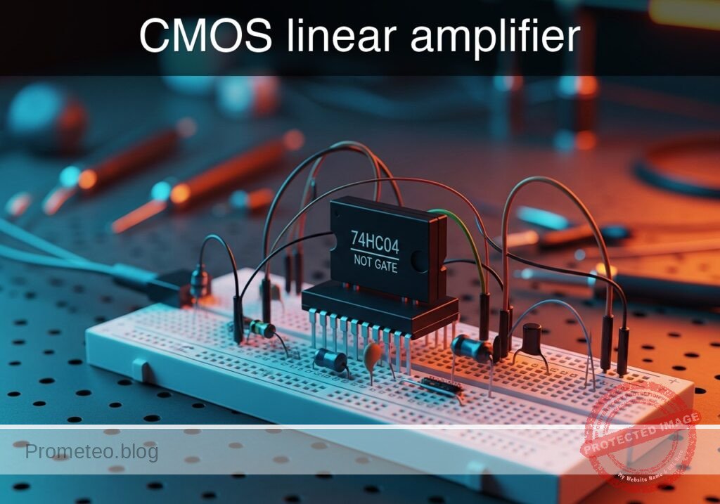
Level: Advanced. Configure a 74HC04 inverter as a Class A linear analog amplifier using negative feedback.
Objective and use case
You will construct a single-stage voltage amplifier using one inverter gate from a 74HC04 IC, biased into its linear region via a feedback resistor. This configuration forces the digital gate to act as an analog inverting amplifier for small AC signals.
Why it is useful:
* Internal structure analysis: Demonstrates that digital logic gates are constructed from analog transistors (MOSFETs) and possess an active linear region.
* Crystal oscillators: This topology is the fundamental building block for Pierce oscillators used in clock generation.
* Low-cost amplification: Provides a simple, cheap high-impedance amplifier for piezoelectric sensors or microphones without requiring a dedicated Op-Amp.
* Signal buffering: Can be used to square up «lazy» analog edges into sharp digital pulses if the feedback is adjusted.
Expected outcome:
* Self-biasing: The input and output DC voltage settles automatically at approximately VCC / 2 (e.g., ~2.5 V).
* Amplification: An input sine wave of 50 mVpp results in an amplified inverted output sine wave.
* Linearity: The output signal replicates the input shape without clipping (provided the input signal remains small).
Target audience and level:
Electronic engineering students and analog system designers (Level: Advanced).
Materials
- U1: 74HC04 (Hex Inverter), function: active amplification element.
- Rf: 1 MΩ resistor, function: negative feedback for DC biasing (Class A operation).
- Cin: 100 nF ceramic capacitor, function: AC coupling for input signal.
- Cout: 10 µF electrolytic capacitor, function: AC coupling for load.
- RL: 10 kΩ resistor, function: output load simulation.
- V1: 5 V DC supply, function: main power source.
- V_SIG: Signal generator, function: 1 kHz sine wave, 50 mVpp (with 0 V DC offset).
Pin-out of the IC used
Chip: 74HC04 (Hex Inverter)
| Pin | Name | Logic function | Connection in this case |
|---|---|---|---|
| 1 | 1 A | Inverter 1 Input | Connected to GATE_IN |
| 2 | 1Y | Inverter 1 Output | Connected to GATE_OUT |
| 7 | GND | Ground | Connected to 0 (GND) |
| 14 | VCC | Power Supply | Connected to VCC |
| 3,5,9,11,13 | Inputs | Unused Inputs | Connect to 0 (GND) to prevent oscillation |
Wiring guide
- V1: Positive terminal to
VCC, negative terminal to0. - U1: Pin 14 to
VCC, Pin 7 to0. - Unused Inputs: U1 pins 3, 5, 9, 11, 13 to
0(Essential for stability). - Rf: Connect between
GATE_IN(Pin 1) andGATE_OUT(Pin 2). - Cin: Connect between
VIN_AC(Signal Generator output) andGATE_IN. - U1 Gate: Pin 1 to
GATE_IN, Pin 2 toGATE_OUT. - Cout: Positive terminal to
GATE_OUT, negative terminal toVOUT_LOAD. - RL: Connect between
VOUT_LOADand0. - V_SIG: Output to
VIN_AC, Ground to0.
Conceptual block diagram
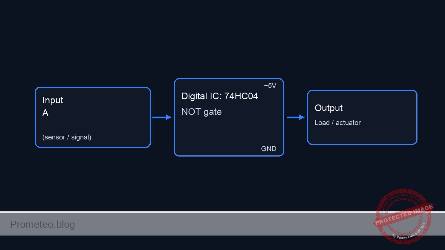
Schematic
Practical case: CMOS linear amplifier

                                            (Feedback Loop)
                                  .-----------[ Rf: 1 MΩ ]------------.
                                  |                                   |
                                  V                                   |
[ V_SIG ] --(Signal)--> [ Cin: 100nF ] --(Pin 1)--> [ U1: 74HC04 ] --(Pin 2)--> [ Cout: 10µF ] --> [ RL: 10 kΩ ] --> GND
                                                          ^
                                                          |
                                                 [ Power: 5 V / GND ]
                                                 [ Unused Pins: 0 V ]
Truth table
Although operated as an analog amplifier, the 74HC04 maintains its digital truth table logic if driven rail-to-rail.
| Input (A) | Output (Y) |
|---|---|
| L (0 V) | H (5 V) |
| H (5 V) | L (0 V) |
Measurements and tests
-
DC Bias Check:
- Disconnect
V_SIGtemporarily. - Measure the DC voltage at
GATE_INandGATE_OUT. - Validation: Both should measure approximately VCC / 2 (around 2.5 V). This confirms the feedback resistor Rf has correctly biased the inverter into the transition region.
- Disconnect
-
AC Gain Measurement:
- Reconnect
V_SIG(1 kHz, sine, 50 mVpp). - Use an oscilloscope to observe Channel 1 at
VIN_ACand Channel 2 atGATE_OUT. - Validation: Calculate Voltage Gain Av = Voutpp / Vinpp. You should observe an inverted sine wave with significant gain (typically 10x to 100x depending on the specific manufacturer of the 74HC04).
- Reconnect
-
Linearity Limit:
- Slowly increase the amplitude of
V_SIG. - Validation: Observe the point where the output sine wave flattens at the top (near 5 V) and bottom (near 0 V). This is the dynamic range limit.
- Slowly increase the amplitude of
SPICE netlist and simulation
Reference SPICE Netlist (ngspice) — excerptFull SPICE netlist (ngspice)
* Practical case: CMOS linear amplifier
* 74HC04 Hex Inverter Linear Amplifier Configuration

* --- Power Supply ---
* V1: 5V DC supply
V1 VCC 0 DC 5

* --- Signal Generator ---
* V_SIG: 1 kHz sine wave, 50 mVpp (25 mV amplitude), 0 V DC offset
V_SIG VIN_AC 0 SIN(0 25m 1k)

* --- Components ---

* Cin: 100 nF ceramic capacitor for AC coupling input
Cin VIN_AC GATE_IN 100n

* Rf: 1 MΩ resistor for negative feedback (DC biasing)
Rf GATE_IN GATE_OUT 1Meg

* U1: 74HC04 Hex Inverter
* ... (truncated in public view) ...
Copy this content into a .cir file and run with ngspice.
* Practical case: CMOS linear amplifier
* 74HC04 Hex Inverter Linear Amplifier Configuration

* --- Power Supply ---
* V1: 5V DC supply
V1 VCC 0 DC 5

* --- Signal Generator ---
* V_SIG: 1 kHz sine wave, 50 mVpp (25 mV amplitude), 0 V DC offset
V_SIG VIN_AC 0 SIN(0 25m 1k)

* --- Components ---

* Cin: 100 nF ceramic capacitor for AC coupling input
Cin VIN_AC GATE_IN 100n

* Rf: 1 MΩ resistor for negative feedback (DC biasing)
Rf GATE_IN GATE_OUT 1Meg

* U1: 74HC04 Hex Inverter
* Instantiated as a subcircuit to strictly follow pinout and wiring guide.
* Pinout: 1=1A, 2=1Y, 3=2A, 4=2Y, 5=3A, 6=3Y, 7=GND, 8=4Y, 9=4A, 10=5Y, 11=5A, 12=6Y, 13=6A, 14=VCC
* Connected: Pin 1->GATE_IN, Pin 2->GATE_OUT, Pin 7->0, Pin 14->VCC
* Unused Inputs (3, 5, 9, 11, 13) connected to 0 (Ground).
* Unused Outputs (4, 6, 8, 10, 12) left as floating nodes (NC_x).
XU1 GATE_IN GATE_OUT 0 NC_2 0 NC_3 0 NC_4 0 NC_5 0 NC_6 0 VCC 74HC04

* Cout: 10 µF electrolytic capacitor for AC coupling load
* Connected from GATE_OUT (approx 2.5V DC) to VOUT_LOAD (0V DC)
Cout GATE_OUT VOUT_LOAD 10u

* RL: 10 kΩ load resistor
RL VOUT_LOAD 0 10k

* --- Subcircuit Models ---

* Subcircuit for 74HC04 Hex Inverter
* Implements 6 inverters using robust continuous behavioral sources (tanh).
* Model assumes Vth = VCC/2.
* Gain factor 100 used to approximate open-loop gain in linear region (~250) while ensuring convergence.
.subckt 74HC04 1 2 3 4 5 6 7 8 9 10 11 12 13 14
* Pin 14 = VCC, Pin 7 = GND
* Inverter 1 (1A->1Y)
B1 2 7 V = V(14,7)/2 + (V(14,7)/2) * tanh(100 * (V(14,7)/2 - V(1,7)))
* Inverter 2 (2A->2Y)
B2 4 7 V = V(14,7)/2 + (V(14,7)/2) * tanh(100 * (V(14,7)/2 - V(3,7)))
* Inverter 3 (3A->3Y)
B3 6 7 V = V(14,7)/2 + (V(14,7)/2) * tanh(100 * (V(14,7)/2 - V(5,7)))
* Inverter 4 (4A->4Y) - Note: Pin 9 is Input, Pin 8 is Output
B4 8 7 V = V(14,7)/2 + (V(14,7)/2) * tanh(100 * (V(14,7)/2 - V(9,7)))
* Inverter 5 (5A->5Y) - Note: Pin 11 is Input, Pin 10 is Output
B5 10 7 V = V(14,7)/2 + (V(14,7)/2) * tanh(100 * (V(14,7)/2 - V(11,7)))
* Inverter 6 (6A->6Y) - Note: Pin 13 is Input, Pin 12 is Output
B6 12 7 V = V(14,7)/2 + (V(14,7)/2) * tanh(100 * (V(14,7)/2 - V(13,7)))
.ends

* --- Analysis Directives ---
* Transient analysis: 5 ms duration to capture multiple 1 kHz cycles.
.tran 10u 5m

* Output variables for batch processing
* INPUT: VIN_AC, OUTPUT: VOUT_LOAD
.print tran V(VIN_AC) V(VOUT_LOAD) V(GATE_IN) V(GATE_OUT)

.op
.end
* --- GPT review (BOM/Wiring/SPICE) ---
* circuit_ok=true
* simulation_summary: The simulation shows a functional inverting amplifier. The input signal (VIN_AC) is a ~25mV amplitude sine wave. The output (VOUT_LOAD) is an inverted sine wave with an amplitude of approximately 2.4V to 2.5V, indicating a very high gain that is causing significant clipping/saturation near the rails (approx +/- 2.5V swing). The DC bias point at GATE_IN and GATE_OUT settles near 2.5V (VCC/2) as expected for this self-biasing topology.
* bom_vs_spice equivalences ignored:
*   - U1 (74HC04) is modeled as a subcircuit using continuous behavioral voltage sources (tanh functions) to approximate the analog transfer curve of CMOS inverters.
* overall_comment: The circuit is a classic example of using a digital CMOS inverter as a linear class A amplifier. The netlist correctly implements the self-biasing scheme (Rf feedback) and AC coupling. The simulation results confirm the high open-loop gain of the HC series inverter, resulting in a heavily clipped output for a 50mVpp input. As a didactic example, it effectively demonstrates the concept, though a teacher might want to reduce the input amplitude or add an input series resistor to reduce the gain if a cleaner sine wave is desired.
* --------------------------------------
Simulation Results (Transient Analysis)

Show raw data table (508 rows)
Index   time            v(vin_ac)       v(vout_load)    v(gate_in)      v(gate_out)
0	0.000000e+00	0.000000e+00	0.000000e+00	2.500000e+00	2.500000e+00
1	1.000000e-07	1.570796e-05	-3.92600e-03	2.500016e+00	2.496074e+00
2	2.000000e-07	3.141592e-05	-7.85100e-03	2.500031e+00	2.492149e+00
3	4.000000e-07	6.283179e-05	-1.56989e-02	2.500063e+00	2.484301e+00
4	8.000000e-07	1.256632e-04	-3.13823e-02	2.500126e+00	2.468618e+00
5	1.600000e-06	2.513232e-04	-6.26967e-02	2.500251e+00	2.437303e+00
6	3.200000e-06	5.026210e-04	-1.25097e-01	2.500501e+00	2.374901e+00
7	6.400000e-06	1.005039e-03	-2.48425e-01	2.500997e+00	2.251567e+00
8	1.280000e-05	2.008453e-03	-4.87825e-01	2.501977e+00	2.012143e+00
9	2.280000e-05	3.569178e-03	-8.34430e-01	2.503471e+00	1.665472e+00
10	3.280000e-05	5.115818e-03	-1.13904e+00	2.504919e+00	1.360762e+00
11	4.280000e-05	6.642268e-03	-1.39785e+00	2.506318e+00	1.101832e+00
12	5.280000e-05	8.142504e-03	-1.61199e+00	2.507667e+00	8.875322e-01
13	6.280000e-05	9.610606e-03	-1.78571e+00	2.508964e+00	7.136492e-01
14	7.280000e-05	1.104078e-02	-1.92461e+00	2.510208e+00	5.745580e-01
15	8.280000e-05	1.242738e-02	-2.03459e+00	2.511395e+00	4.643784e-01
16	9.280000e-05	1.376493e-02	-2.12112e+00	2.512524e+00	3.776434e-01
17	1.028000e-04	1.504816e-02	-2.18894e+00	2.513590e+00	3.096072e-01
18	1.128000e-04	1.627201e-02	-2.24200e+00	2.514591e+00	2.563270e-01
19	1.228000e-04	1.743163e-02	-2.28348e+00	2.515522e+00	2.146211e-01
20	1.328000e-04	1.852246e-02	-2.31590e+00	2.516381e+00	1.819734e-01
21	1.428000e-04	1.954019e-02	-2.34122e+00	2.517164e+00	1.564217e-01
22	1.528000e-04	2.048080e-02	-2.36095e+00	2.517868e+00	1.364514e-01
23	1.628000e-04	2.134059e-02	-2.37626e+00	2.518489e+00	1.209036e-01
... (484 more rows) ...
Common mistakes and how to avoid them
- Using the wrong logic family: Students often use 74LS04 or 74HCT04. These have internal pull-ups or different input thresholds that prevent symmetrical linear biasing. Solution: Ensure you use the 74HC04 (CMOS) or CD4069UB.
- Input signal too large: Applying a standard TTL/CMOS logic signal (0-5 V) will result in a square wave output, not amplification. Solution: Keep the input signal small (under 100 mVpp) to stay within the linear region.
- Floating unused inputs: Leaving pins 3, 5, 9, etc., disconnected causes internal noise and excessive power consumption. Solution: Always tie unused inputs of CMOS chips to Ground (
0).
Troubleshooting
- Symptom: Output is stuck at 0 V or 5 V.
- Cause: Feedback resistor Rf is missing or open circuit.
- Fix: Check continuity of Rf (1 MΩ). It is required to pull the input voltage to the tipping point.
- Symptom: High frequency noise superimposed on the signal.
- Cause: Parasitic oscillation due to high gain and stray capacitance.
- Fix: Shorten wires or add a small capacitor (e.g., 10 pF) in parallel with Rf to reduce bandwidth.
- Symptom: Gain is very low ($< 2$).
- Cause: Load resistance RL is too small.
- Fix: The output impedance of a 74HC04 in linear mode is relatively high. Increase RL to 100 kΩ or remove it for testing.
Possible improvements and extensions
- Crystal Oscillator: Replace the signal generator with a quartz crystal and two load capacitors (to ground) at the input and output pins to create a stable clock source.
- Cascaded Amplifier: Connect the output of the first stage (via a capacitor) to a second identically configured 74HC04 stage to achieve much higher total voltage gain.
More Practical Cases on Prometeo.blog
Find this product and/or books on this topic on Amazon
As an Amazon Associate, I earn from qualifying purchases. If you buy through this link, you help keep this project running.
Quick Quiz

Telecommunications Electronics Engineer and Computer Engineer (official degrees in Spain).