Level: Medium. Compare voltage ripple in a basic power supply by varying filtering capacitance under load.
Objective and use case
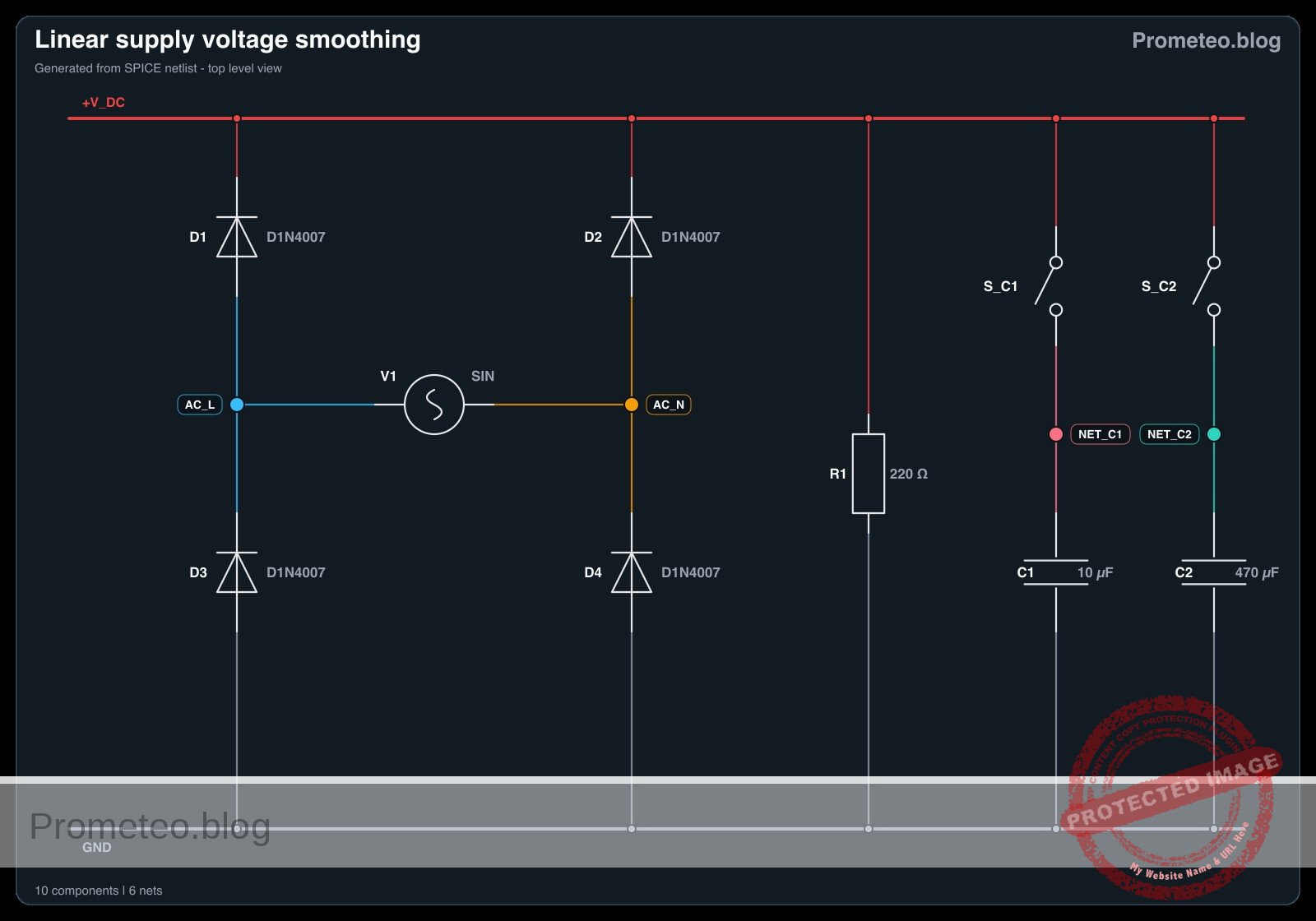
In this practical case, you will build a Full-Wave Bridge Rectifier circuit coupled with a selectable filter capacitor bank and a resistive load. You will analyze how the value of the filter capacitor affects the quality of the DC output by measuring the «ripple» voltage superimposed on the DC signal.
- Audio Power Supplies: Reducing 50/60 Hz hum in amplifiers and speakers.
- Digital Logic Power: Ensuring stable voltage levels to prevent microcontroller resets or erratic behavior.
- Sensor Conditioning: Providing clean DC power to analog sensors for accurate readings.
- Battery Charging: Smoothing the charging current to prolong battery life.
Expected outcome:
* Waveform Transformation: Visual observation of AC sine wave converting to pulsing DC, then to smooth DC.
* Ripple Voltage (Vripple): A high peak-to-peak ripple voltage (> 5 V) with a small capacitor (10 µF).
* Smoothing Effect: A significantly reduced ripple voltage (< 0.5 V) when switching to a large capacitor (470 µF).
* Target Audience: Intermediate electronics students and hobbyists familiar with AC/DC concepts.
Materials
- V1: 12 V (RMS) AC transformer secondary or AC function generator (60 Hz), function: AC power source.
- D1: 1N4007 Diode, function: Bridge rectifier top-left.
- D2: 1N4007 Diode, function: Bridge rectifier top-right.
- D3: 1N4007 Diode, function: Bridge rectifier bottom-left.
- D4: 1N4007 Diode, function: Bridge rectifier bottom-right.
- R1: 220 Ω resistor (2 Watt rating recommended), function: Static Load.
- C1: 10 µF electrolytic capacitor (25 V or higher), function: Low-value filter.
- C2: 470 µF electrolytic capacitor (25 V or higher), function: High-value filter.
- S1: SPDT Switch or jumper wire, function: Selects between C1 and C2.
- Test Equipment: Oscilloscope (preferred) or Multimeter with AC/DC measurement capabilities.
Wiring guide
Construct the circuit using the following node connections. Ensure electrolytic capacitors are connected with correct polarity (Positive terminal to V_DC, Negative terminal to 0 / GND).
- V1 (Source): Connects between node
AC_Land nodeAC_N. - D1: Anode connects to
AC_L, Cathode connects toV_DC. - D2: Anode connects to
AC_N, Cathode connects toV_DC. - D3: Anode connects to
0(GND), Cathode connects toAC_L. - D4: Anode connects to
0(GND), Cathode connects toAC_N. - R1 (Load): Connects between node
V_DCand node0(GND). - C1 (Test Case A): Positive terminal to
V_DC, Negative terminal to0(GND). - C2 (Test Case B): Positive terminal to
V_DC, Negative terminal to0(GND) (Replace C1 with C2 for second test).
Conceptual block diagram
Schematic
[ INPUT SOURCE ]              [ RECTIFICATION ]                [ FILTER STAGE ]                 [ OUTPUT LOAD ]

                                                                  +-> [ Capacitor C1 ] -+
                                                                  |     (10 uF)         |
 [ AC Source V1 ] --(12 V AC)--> [ Bridge Rectifier ] --(Raw DC)-->+                     +--(V_DC)--> [ Load Resistor R1 ]
    (12 V RMS)                   [  D1, D2, D3, D4  ]              |   [ Switch S1  ]    |            (220 Ohm)
                                                                  +-> [ Capacitor C2 ] -+                |
                                                                        (470 uF)                         |
                                                                                                         |
                                                                                                         v
                                                                                                  [ Oscilloscope ]
                                                                                                  (Measure Ripple)
Electrical diagram
Measurements and tests
Follow these steps to validate the smoothing efficiency:
- Baseline (No Capacitor): Temporarily remove any capacitor. Measure
V_DCwith an oscilloscope. You should see a full-wave rectified signal (humps going to 0 V) at 120 Hz (or 100 Hz). - Small Capacitor Test (C1 = 10 µ F):
- Insert $C1$.
- Measure the peak voltage (Vpeak) and the minimum valley voltage (Vmin).
- Calculate Ripple: Vripple = Vpeak – Vmin.
- Expectation: Significant sawtooth ripple (fast discharge).
- Large Capacitor Test (C2 = 470 µ F):
- Replace $C1$ with $C2$.
- Measure Vpeak and Vmin again.
- Expectation: The DC line is much flatter; Vmin stays close to Vpeak.
- DC Average: Switch your multimeter to DC Volts. Compare the reading of $C1$ vs $C2$. The average voltage with $C2$ will be higher because the capacitor maintains the charge longer.
SPICE netlist and simulation
Reference SPICE Netlist (ngspice) — excerptFull SPICE netlist (ngspice)
* Linear supply voltage smoothing
*
* Description:
* This netlist simulates a full-wave bridge rectifier power supply with a
* selectable smoothing capacitor.
* - 0ms to 100ms: C1 (10uF) is connected (High Ripple case).
* - 100ms to 200ms: C2 (470uF) is connected (Low Ripple case), simulating
*   switch S1 toggling.
*
* Connections:
* V1 (AC Source) -> Nodes AC_L, AC_N
* D1-D4 (Bridge) -> Nodes AC_L, AC_N, V_DC, 0 (GND)
* R1 (Load)      -> Nodes V_DC, 0
* S1 (Switch)    -> Modeled via S_C1 and S_C2 connecting V_DC to C1/C2
*
* -----------------------------------------------------------------------------

* --- AC Power Source ---
* 12V RMS AC, 60Hz.
* Peak Voltage = 12 * sqrt(2) = 16.97 V
* ... (truncated in public view) ...
Copy this content into a .cir file and run with ngspice.
* Linear supply voltage smoothing
*
* Description:
* This netlist simulates a full-wave bridge rectifier power supply with a
* selectable smoothing capacitor.
* - 0ms to 100ms: C1 (10uF) is connected (High Ripple case).
* - 100ms to 200ms: C2 (470uF) is connected (Low Ripple case), simulating
*   switch S1 toggling.
*
* Connections:
* V1 (AC Source) -> Nodes AC_L, AC_N
* D1-D4 (Bridge) -> Nodes AC_L, AC_N, V_DC, 0 (GND)
* R1 (Load)      -> Nodes V_DC, 0
* S1 (Switch)    -> Modeled via S_C1 and S_C2 connecting V_DC to C1/C2
*
* -----------------------------------------------------------------------------

* --- AC Power Source ---
* 12V RMS AC, 60Hz.
* Peak Voltage = 12 * sqrt(2) = 16.97 V
V1 AC_L AC_N SIN(0 16.97 60)

* --- Bridge Rectifier (1N4007) ---
* D1: Anode=AC_L, Cathode=V_DC
D1 AC_L V_DC D1N4007
* D2: Anode=AC_N, Cathode=V_DC
D2 AC_N V_DC D1N4007
* D3: Anode=GND, Cathode=AC_L
D3 0 AC_L D1N4007
* D4: Anode=GND, Cathode=AC_N
D4 0 AC_N D1N4007

* --- Load Resistor ---
* 220 Ohm resistor across the DC output
R1 V_DC 0 220

* --- Filter Capacitors & Switching Logic ---
* We simulate the SPDT switch S1 by using two voltage-controlled switches.
* S_C1 connects V_DC to C1. S_C2 connects V_DC to C2.
* Control signals ensure only one is active at a time (break-before-make effectively).

* Capacitor C1 (10uF) path
S_C1 V_DC NET_C1 CTRL_C1 0 SW_MODEL
C1 NET_C1 0 10u

* Capacitor C2 (470uF) path
S_C2 V_DC NET_C2 CTRL_C2 0 SW_MODEL
C2 NET_C2 0 470u

* --- Control Signals (Dynamic Stimuli) ---
* CTRL_C1: Starts High (5V), goes Low (0V) at 100ms.
* Keeps C1 connected for the first 100ms.
V_CTRL_C1 CTRL_C1 0 PULSE(5 0 100m 1u 1u 1 2)

* CTRL_C2: Starts Low (0V), goes High (5V) at 100ms.
* Connects C2 for the remainder of the simulation.
V_CTRL_C2 CTRL_C2 0 PULSE(0 5 100m 1u 1u 1 2)

* --- Component Models ---
* Generic model for 1N4007 Power Diode
.model D1N4007 D(IS=7.03n RS=0.034 N=1.8 BV=1000 IBV=5u CJO=10p TT=100n)

* Ideal Switch Model (Threshold=2.5V, On-Res=10mOhm, Off-Res=100MegOhm)
.model SW_MODEL SW(Vt=2.5 Ron=0.01 Roff=100Meg)

* --- Analysis Directives ---
* Transient analysis: 200ms total time, 50us step size.
* This captures approx 6 cycles with C1 and 6 cycles with C2.
.tran 50u 200m

* Print directives for simulation log/plotting
.print tran V(V_DC) V(AC_L) V(AC_N)

.end
Simulation Results (Transient Analysis)

Show raw data table (4050 rows)
Index   time            v(v_dc)         v(ac_l)         v(ac_n)
0	0.000000e+00	6.658603e-23	4.156609e-18	4.156609e-18
1	5.000000e-07	1.885342e-19	1.599385e-03	-1.59938e-03
2	1.000000e-06	6.893339e-12	3.198770e-03	-3.19877e-03
3	2.000000e-06	3.416858e-11	6.397539e-03	-6.39754e-03
4	4.000000e-06	1.718574e-10	1.279507e-02	-1.27951e-02
5	8.000000e-06	9.966330e-10	2.559012e-02	-2.55901e-02
6	1.325366e-05	3.861142e-09	4.239524e-02	-4.23952e-02
7	2.095388e-05	1.446061e-08	6.702595e-02	-6.70259e-02
8	3.129676e-05	5.099200e-08	1.001088e-01	-1.00109e-01
9	4.482862e-05	1.835180e-07	1.433897e-01	-1.43390e-01
10	6.128867e-05	6.888081e-07	1.960312e-01	-1.96031e-01
11	8.042390e-05	2.827323e-06	2.572195e-01	-2.57217e-01
12	1.019046e-04	1.303092e-05	3.258956e-01	-3.25883e-01
13	1.254895e-04	6.815023e-05	4.012964e-01	-4.01228e-01
14	1.509795e-04	4.024321e-04	4.828893e-01	-4.82487e-01
15	1.782228e-04	2.626479e-03	5.709779e-01	-5.68351e-01
16	2.071492e-04	1.723315e-02	6.705660e-01	-6.53333e-01
17	2.380619e-04	8.388777e-02	8.024272e-01	-7.18539e-01
18	2.734880e-04	2.529945e-01	9.997734e-01	-7.46779e-01
19	3.097680e-04	4.785526e-01	1.227902e+00	-7.49349e-01
20	3.521718e-04	7.463483e-01	1.496384e+00	-7.50036e-01
21	3.938443e-04	1.008721e+00	1.759554e+00	-7.50833e-01
22	4.438443e-04	1.322891e+00	2.074586e+00	-7.51694e-01
23	4.938443e-04	1.636032e+00	2.388601e+00	-7.52568e-01
... (4026 more rows) ...
Reference SPICE netlist (ngspice)
* Linear supply voltage smoothing
*
* Description:
* This netlist simulates a full-wave bridge rectifier power supply with a
* selectable smoothing capacitor.
* - 0ms to 100ms: C1 (10uF) is connected (High Ripple case).
* - 100ms to 200ms: C2 (470uF) is connected (Low Ripple case), simulating
*   switch S1 toggling.
*
* Connections:
* V1 (AC Source) -> Nodes AC_L, AC_N
* D1-D4 (Bridge) -> Nodes AC_L, AC_N, V_DC, 0 (GND)
* R1 (Load)      -> Nodes V_DC, 0
* S1 (Switch)    -> Modeled via S_C1 and S_C2 connecting V_DC to C1/C2
*
* -----------------------------------------------------------------------------

* --- AC Power Source ---
* 12V RMS AC, 60Hz.
* Peak Voltage = 12 * sqrt(2) = 16.97 V
V1 AC_L AC_N SIN(0 16.97 60)

* --- Bridge Rectifier (1N4007) ---
* D1: Anode=AC_L, Cathode=V_DC
D1 AC_L V_DC D1N4007
* D2: Anode=AC_N, Cathode=V_DC
D2 AC_N V_DC D1N4007
* D3: Anode=GND, Cathode=AC_L
D3 0 AC_L D1N4007
* D4: Anode=GND, Cathode=AC_N
D4 0 AC_N D1N4007

* --- Load Resistor ---
* 220 Ohm resistor across the DC output
R1 V_DC 0 220

* --- Filter Capacitors & Switching Logic ---
* We simulate the SPDT switch S1 by using two voltage-controlled switches.
* S_C1 connects V_DC to C1. S_C2 connects V_DC to C2.
* Control signals ensure only one is active at a time (break-before-make effectively).

* Capacitor C1 (10uF) path
S_C1 V_DC NET_C1 CTRL_C1 0 SW_MODEL
C1 NET_C1 0 10u

* Capacitor C2 (470uF) path
S_C2 V_DC NET_C2 CTRL_C2 0 SW_MODEL
C2 NET_C2 0 470u

* --- Control Signals (Dynamic Stimuli) ---
* CTRL_C1: Starts High (5V), goes Low (0V) at 100ms.
* Keeps C1 connected for the first 100ms.
V_CTRL_C1 CTRL_C1 0 PULSE(5 0 100m 1u 1u 1 2)

* CTRL_C2: Starts Low (0V), goes High (5V) at 100ms.
* Connects C2 for the remainder of the simulation.
V_CTRL_C2 CTRL_C2 0 PULSE(0 5 100m 1u 1u 1 2)

* --- Component Models ---
* Generic model for 1N4007 Power Diode
.model D1N4007 D(IS=7.03n RS=0.034 N=1.8 BV=1000 IBV=5u CJO=10p TT=100n)

* Ideal Switch Model (Threshold=2.5V, On-Res=10mOhm, Off-Res=100MegOhm)
.model SW_MODEL SW(Vt=2.5 Ron=0.01 Roff=100Meg)

* --- Analysis Directives ---
* Transient analysis: 200ms total time, 50us step size.
* This captures approx 6 cycles with C1 and 6 cycles with C2.
.tran 50u 200m

* Print directives for simulation log/plotting
.print tran V(V_DC) V(AC_L) V(AC_N)

.end
Simulation Results (Transient Analysis)
Common mistakes and how to avoid them
- Reversed Capacitor Polarity: Electrolytic capacitors will explode if connected backwards. Solution: Ensure the side marked with a stripe (negative) connects to the
0(GND) node and the other side to the positive rectifier output. - Under-rated Resistor Power: A 220 Ω resistor at ~15 V DC dissipates about 1 Watt (P = V^2 / R). Using a standard 1/4 W resistor will burn it. Solution: Use a power resistor (2 W+) or increase resistance to 1 kΩ (though this reduces ripple visibility).
- Measuring Ripple on DC Setting: A standard multimeter on DC mode averages the voltage, hiding the ripple. Solution: Use an oscilloscope for visual analysis, or set the multimeter to AC mode to measure the RMS value of the ripple component only.
Troubleshooting
- Symptom: No output voltage at
V_DC.- Cause: AC source not on or bridge diodes open/connected incorrectly.
- Fix: Check V1 output and verify diode orientation (ring marks on cathodes).
- Symptom: Ripple does not change when swapping capacitors.
- Cause: Load resistor $R1$ is missing or open circuit. Without a load, the capacitor has no path to discharge, so voltage stays at peak regardless of capacitance.
- Fix: Ensure $R1$ is securely connected parallel to the capacitor.
- Symptom: Fuse blows or transformer hums loudly.
- Cause: Short circuit in the bridge (e.g., D1 and D3 shorting AC mains).
- Fix: Power off immediately and check wiring. Ensure
AC_LandAC_Nare not directly connected to0or each other.
Possible improvements and extensions
- Voltage Regulator: Add an LM7812 or LM317 linear regulator after the capacitor to see how active regulation eliminates the remaining ripple.
- RC Pi Filter: Add a series resistor and a second capacitor ($C-R-C$) to create a passive low-pass filter, further reducing ripple without active components (at the cost of voltage drop).
More Practical Cases on Prometeo.blog
Find this product and/or books on this topic on Amazon
As an Amazon Associate, I earn from qualifying purchases. If you buy through this link, you help keep this project running.
Quick Quiz

Telecommunications Electronics Engineer and Computer Engineer (official degrees in Spain).