Level: Medium – Build a receiver capable of demodulating an audio signal transmitted via an LED light beam using a photodiode.
Objective and use case
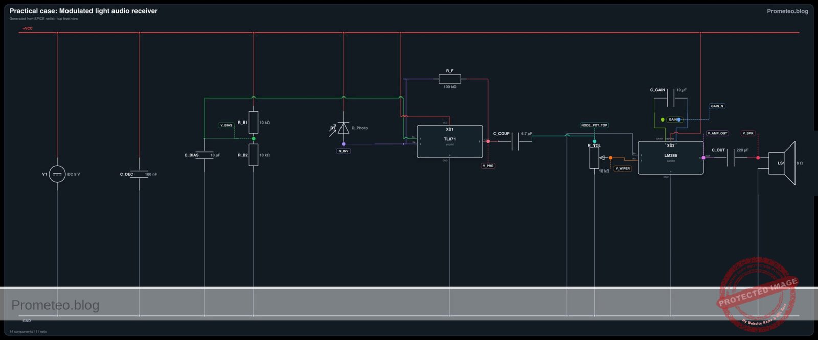
In this practical case, you will build an analog optical receiver using a high-speed photodiode configured in photoconductive mode, followed by a Transimpedance Amplifier (TIA) and an audio power amplifier. This circuit detects changes in light intensity modulated by an audio source and converts them back into electrical signals to drive a speaker.
Why it is useful:
* Optical Wireless Communication (OWC): Demonstrates the fundamental physics behind Li-Fi and infrared remote controls.
* Galvanic Isolation: Allows audio transmission between devices without a physical ground connection, preventing ground loops.
* Security: Unlike radio frequency (RF), optical signals are confined to the room and cannot pass through opaque walls.
* Interference Immunity: Immune to electromagnetic interference (EMI) that typically affects copper wire transmission.
Expected outcome:
* Signal Output: A measurable voltage waveform at the TIA output (V_PRE) that mirrors the transmitted audio waveform.
* Audio Output: Clear sound reproduction through the loudspeaker (LS1) when the photodiode receives modulated light.
* Voltage Levels: The TIA output should ride on a DC bias (approx. VCC/2) with an AC signal swing depending on light intensity.
* Volume Control: Adjustment of the audio level via the potentiometer (R_VOL).
Target audience: Electronics students and hobbyists interested in analog signal conditioning.
Materials
- V1: 9 V DC voltage source, function: Main circuit power supply.
- D1: BPW34 Photodiode, function: Optical sensor (light to current converter).
- U1: TL071 Operational Amplifier, function: Transimpedance Amplifier (TIA).
- U2: LM386N-1 Audio Amplifier IC, function: Power amplification for speaker.
- R_F: 100 kΩ resistor, function: TIA feedback resistor (sets gain).
- R_B1: 10 kΩ resistor, function: Voltage divider top for VCC/2 bias.
- R_B2: 10 kΩ resistor, function: Voltage divider bottom for VCC/2 bias.
- R_VOL: 10 kΩ potentiometer, function: Audio volume control.
- C_DEC: 100 nF ceramic capacitor, function: Power supply decoupling.
- C_BIAS: 10 µF electrolytic capacitor, function: Stabilize VCC/2 bias point.
- C_COUP: 4.7 µF electrolytic capacitor, function: DC blocking between TIA and Audio Amp.
- C_OUT: 220 µF electrolytic capacitor, function: Output coupling for speaker.
- C_GAIN: 10 µF electrolytic capacitor, function: LM386 gain setting (Pins 1-8).
- LS1: 8 Ω / 0.5W Speaker, function: Audio transducer.
Wiring guide
This guide defines the connections using specific SPICE node names: VCC, 0 (GND), V_BIAS, N_INV (Inverting input), V_PRE (Pre-amp out), V_WIPER (Potentiometer out), and V_SPK (Amp out).
Power and Bias:
* V1: Positive terminal to VCC, Negative terminal to 0.
* R_B1: Connects between VCC and V_BIAS.
* R_B2: Connects between V_BIAS and 0.
* C_BIAS: Positive lead to V_BIAS, Negative lead to 0.
* C_DEC: Connects between VCC and 0 (near U1).
Transimpedance Amplifier (Stage 1):
* U1 (Op-Amp): V+ pin to VCC, V- pin to 0. Non-inverting input (+) to V_BIAS. Inverting input (-) to N_INV. Output pin to V_PRE.
* D1 (Photodiode): Cathode to VCC, Anode to N_INV (Reverse biased).
* R_F: Connects between N_INV and V_PRE.
Signal Coupling:
* C_COUP: Positive lead to V_PRE, Negative lead to NODE_POT_TOP.
* R_VOL: Top terminal to NODE_POT_TOP, Bottom terminal to 0, Wiper to V_WIPER.
Power Amplifier (Stage 2):
* U2 (LM386): Vs (Pin 6) to VCC, GND (Pin 4) to 0. Non-inverting Input (Pin 3) to V_WIPER. Inverting Input (Pin 2) to 0.
* C_GAIN: Connects between Pin 1 and Pin 8 of U2 (Positive to Pin 1).
* C_OUT: Positive lead to U2 Output (Pin 5), Negative lead to V_SPK.
* LS1: Connects between V_SPK and 0.
Conceptual block diagram

Schematic
Title: Practical case: Modulated light audio receiver

      [ INPUT / SENSOR ]               [ STAGE 1: TIA PRE-AMP ]                  [ INTERSTAGE ]                [ STAGE 2: POWER AMP ]              [ OUTPUT ]

                                     +-----------[ R_F: 100k ]-----------+
                                     |           (Feedback)              |
                                     v                                   |
(Light) ~~~> [ D1: BPW34 ] --(I)--> [ (-) N_INV      U1: TL071      OUT ] --(V_PRE)--> [ C_COUP ] --> [ R_VOL: 10k ] --(V_WIPER)-->+
             (Photodiode)           |                                    |             (4.7uF)        (Volume Pot)                 |
                                    | (+) V_BIAS                         |                                                         |
                                    +----------------^-------------------+                                                         |
                                                     |                                                                             |
      [ POWER & BIAS ]                               |                                                                             v
                                                     |                                                                     [ IN+  U2: LM386  OUT ] --(V_SPK)--> [ C_OUT ] --> [ LS1: Speaker ]
    [ V1: 9 V DC Source ] --(VCC)--> (Powers U1, U2)  |                                                                     |                 |                (220uF)        (8 Ohm)
             |                                       |                                                                     |  Gain Pins 1-8  |                                  |
             +---> [ Bias Divider ] --(VCC/2 Ref)----+                                                                     +--------+--------+                                 GND
                   (R_B1, R_B2,                                                                                                     |
                    C_BIAS)                                                                                                    [ C_GAIN ]
                                                                                                                                (10uF)
Electrical diagram
Measurements and tests
- Bias Point Check: Use a multimeter to measure the voltage at node
V_BIAS. It should be approximately 4.5 V (half of VCC). If not, check R_B1 and R_B2. - Ambient Light Level: Measure the DC voltage at
V_PREwithout any modulated signal (just ambient light). It should be slightly lower thanV_BIASdepending on the ambient brightness hitting D1. - Signal Acquisition:
- Point a modulated light source (e.g., an LED connected to an audio output or a signal generator) at D1.
- Use an oscilloscope at
V_PRE. You should see an AC waveform superimposed on the DC level. - Measure the Vpp (Peak-to-Peak Voltage). It should be in the range of 100 mV to 1 V depending on the distance and light intensity.
- Audio Test: Turn R_VOL up slowly. You should hear the transmitted audio clearly from LS1.
SPICE netlist and simulation
Reference SPICE Netlist (ngspice) — excerptFull SPICE netlist (ngspice)
* Practical case: Modulated light audio receiver

* --- Component Models ---
* Generic Photodiode Model
.model D_BPW34 D(Is=1n Rs=5 Cjo=10p)

* --- Subcircuits ---

* TL071 Operational Amplifier Macro Model
* Pinout: 1=NonInv 2=Inv 3=V+ 4=V- 5=Out
.SUBCKT TL071 P_NI P_INV P_VCC P_VEE P_OUT
  * Input Impedance
  Rin P_NI P_INV 1T
  * Output Stage (Behavioral with Rail Limiting)
  * Models high open-loop gain and saturation at Rails +/- 1.5V
  B1 P_OUT 0 V=V(P_VEE) + 1.5 + (V(P_VCC)-V(P_VEE)-3) * (1 / (1 + exp(-100000 * (V(P_NI)-V(P_INV)))))
.ENDS TL071

* LM386 Audio Amplifier Macro Model
* Pinout: 1=Gain 2=Inv 3=NonInv 4=GND 5=Out 6=Vs 8=Gain
* ... (truncated in public view) ...
Copy this content into a .cir file and run with ngspice.
* Practical case: Modulated light audio receiver

* --- Component Models ---
* Generic Photodiode Model
.model D_BPW34 D(Is=1n Rs=5 Cjo=10p)

* --- Subcircuits ---

* TL071 Operational Amplifier Macro Model
* Pinout: 1=NonInv 2=Inv 3=V+ 4=V- 5=Out
.SUBCKT TL071 P_NI P_INV P_VCC P_VEE P_OUT
  * Input Impedance
  Rin P_NI P_INV 1T
  * Output Stage (Behavioral with Rail Limiting)
  * Models high open-loop gain and saturation at Rails +/- 1.5V
  B1 P_OUT 0 V=V(P_VEE) + 1.5 + (V(P_VCC)-V(P_VEE)-3) * (1 / (1 + exp(-100000 * (V(P_NI)-V(P_INV)))))
.ENDS TL071

* LM386 Audio Amplifier Macro Model
* Pinout: 1=Gain 2=Inv 3=NonInv 4=GND 5=Out 6=Vs 8=Gain
.SUBCKT LM386 P_G1 P_INV P_NI P_GND P_OUT P_VS P_G8
  * Internal Gain Resistor (1.35k) connecting Pins 1 and 8
  R_GAIN_INT P_G1 P_G8 1.35k
  * High resistance to GND to prevent floating node errors for the Gain capacitor
  R_C1 P_G1 0 100Meg
  R_C8 P_G8 0 100Meg

  * Audio Amplifier Behavioral Source
  * Self-biasing output to Vs/2
  * Fixed Gain approx 200 (Assuming C_GAIN is present externally)
  B_OUT P_OUT P_GND V=V(P_VS)/2 + 200*(V(P_NI)-V(P_INV))
.ENDS LM386

* --- Main Circuit ---

* Power Supply (9V)
V1 VCC 0 DC 9

* Power Supply Decoupling
C_DEC VCC 0 100n

* Bias Voltage Generator (VCC/2)
R_B1 VCC V_BIAS 10k
R_B2 V_BIAS 0 10k
C_BIAS V_BIAS 0 10u

* --- Stage 1: Transimpedance Amplifier (TIA) ---
* U1 TL071 Op-Amp
* Connections: NI=V_BIAS, INV=N_INV, V+=VCC, V-=0, OUT=V_PRE
XU1 V_BIAS N_INV VCC 0 V_PRE TL071

* Photodiode Sensor (Reverse Biased)
* Cathode to VCC, Anode to N_INV
D1 N_INV VCC D_BPW34

* Optical Signal Simulation
* Current source representing modulated light (1kHz square wave)
* Connected parallel to photodiode (Anode to Cathode current flow)
I_LIGHT N_INV VCC PULSE(0 2u 0 1u 1u 500u 1000u)

* Feedback Resistor
R_F N_INV V_PRE 100k

* --- Signal Coupling ---
* DC Blocking Capacitor
C_COUP V_PRE NODE_POT_TOP 4.7u

* Volume Potentiometer (10k)
* Modeled as voltage divider. Wiper set to 20% to manage gain.
* Top Resistor (8k)
R_VOL_TOP NODE_POT_TOP V_WIPER 8k
* Bottom Resistor (2k)
R_VOL_BOT V_WIPER 0 2k

* --- Stage 2: Power Amplifier ---
* U2 LM386 Audio Amp
* Connections: 1=GAIN_P, 2=0, 3=V_WIPER, 4=0, 5=V_AMP_OUT, 6=VCC, 8=GAIN_N
XU2 GAIN_P 0 V_WIPER 0 V_AMP_OUT VCC GAIN_N LM386

* Gain Setting Capacitor (Pins 1-8)
C_GAIN GAIN_P GAIN_N 10u

* Output Coupling Capacitor
C_OUT V_AMP_OUT V_SPK 220u

* Speaker Load (8 Ohm)
LS1 V_SPK 0 8

* --- Simulation Directives ---
* Transient analysis for 5ms to see 5 cycles of 1kHz audio
.tran 10u 5ms

* Output data for plotting
.print tran V(V_PRE) V(V_WIPER) V(V_SPK)

.end
Simulation Results (Transient Analysis)

Show raw data table (623 rows)
Index   time            v(v_pre)        v(v_wiper)      v(v_spk)
0	0.000000e+00	4.499900e+00	0.000000e+00	0.000000e+00
1	1.000000e-08	4.501899e+00	3.998838e-04	7.997676e-02
2	1.083984e-08	4.502067e+00	4.334770e-04	8.669540e-02
3	1.251953e-08	4.502403e+00	5.006638e-04	1.001328e-01
4	1.587889e-08	4.503075e+00	6.350376e-04	1.270075e-01
5	2.259763e-08	4.504418e+00	9.037850e-04	1.807570e-01
6	3.603509e-08	4.507106e+00	1.441280e-03	2.882560e-01
7	6.291003e-08	4.512481e+00	2.516269e-03	5.032538e-01
8	1.166599e-07	4.523231e+00	4.666245e-03	9.332491e-01
9	2.241596e-07	4.544731e+00	8.966191e-03	1.793238e+00
10	4.391591e-07	4.587730e+00	1.756605e-02	3.513210e+00
11	8.691581e-07	4.673729e+00	3.476566e-02	6.953131e+00
12	1.000000e-06	4.699898e+00	3.999919e-02	7.999838e+00
13	1.086000e-06	4.699898e+00	3.999923e-02	7.999847e+00
14	1.257999e-06	4.699898e+00	3.999909e-02	7.999818e+00
15	1.601999e-06	4.699898e+00	3.999879e-02	7.999759e+00
16	2.289997e-06	4.699898e+00	3.999821e-02	7.999642e+00
17	3.665994e-06	4.699898e+00	3.999704e-02	7.999408e+00
18	6.417987e-06	4.699898e+00	3.999470e-02	7.998939e+00
19	1.192197e-05	4.699898e+00	3.999001e-02	7.998002e+00
20	2.192197e-05	4.699898e+00	3.998151e-02	7.996300e+00
21	3.192197e-05	4.699898e+00	3.997300e-02	7.994598e+00
22	4.192197e-05	4.699898e+00	3.996450e-02	7.992895e+00
23	5.192197e-05	4.699898e+00	3.995599e-02	7.991193e+00
... (599 more rows) ...
Reference SPICE netlist (ngspice)
* Practical case: Modulated light audio receiver

* --- Component Models ---
* Generic Photodiode Model
.model D_BPW34 D(Is=1n Rs=5 Cjo=10p)

* --- Subcircuits ---

* TL071 Operational Amplifier Macro Model
* Pinout: 1=NonInv 2=Inv 3=V+ 4=V- 5=Out
.SUBCKT TL071 P_NI P_INV P_VCC P_VEE P_OUT
  * Input Impedance
  Rin P_NI P_INV 1T
  * Output Stage (Behavioral with Rail Limiting)
  * Models high open-loop gain and saturation at Rails +/- 1.5V
  B1 P_OUT 0 V=V(P_VEE) + 1.5 + (V(P_VCC)-V(P_VEE)-3) * (1 / (1 + exp(-100000 * (V(P_NI)-V(P_INV)))))
.ENDS TL071

* LM386 Audio Amplifier Macro Model
* Pinout: 1=Gain 2=Inv 3=NonInv 4=GND 5=Out 6=Vs 8=Gain
.SUBCKT LM386 P_G1 P_INV P_NI P_GND P_OUT P_VS P_G8
  * Internal Gain Resistor (1.35k) connecting Pins 1 and 8
  R_GAIN_INT P_G1 P_G8 1.35k
  * High resistance to GND to prevent floating node errors for the Gain capacitor
  R_C1 P_G1 0 100Meg
  R_C8 P_G8 0 100Meg

  * Audio Amplifier Behavioral Source
  * Self-biasing output to Vs/2
  * Fixed Gain approx 200 (Assuming C_GAIN is present externally)
  B_OUT P_OUT P_GND V=V(P_VS)/2 + 200*(V(P_NI)-V(P_INV))
.ENDS LM386

* --- Main Circuit ---

* Power Supply (9V)
V1 VCC 0 DC 9

* Power Supply Decoupling
C_DEC VCC 0 100n

* Bias Voltage Generator (VCC/2)
R_B1 VCC V_BIAS 10k
R_B2 V_BIAS 0 10k
C_BIAS V_BIAS 0 10u

* --- Stage 1: Transimpedance Amplifier (TIA) ---
* U1 TL071 Op-Amp
* Connections: NI=V_BIAS, INV=N_INV, V+=VCC, V-=0, OUT=V_PRE
XU1 V_BIAS N_INV VCC 0 V_PRE TL071

* Photodiode Sensor (Reverse Biased)
* Cathode to VCC, Anode to N_INV
D1 N_INV VCC D_BPW34

* Optical Signal Simulation
* Current source representing modulated light (1kHz square wave)
* Connected parallel to photodiode (Anode to Cathode current flow)
I_LIGHT N_INV VCC PULSE(0 2u 0 1u 1u 500u 1000u)

* Feedback Resistor
R_F N_INV V_PRE 100k

* --- Signal Coupling ---
* DC Blocking Capacitor
C_COUP V_PRE NODE_POT_TOP 4.7u

* Volume Potentiometer (10k)
* Modeled as voltage divider. Wiper set to 20% to manage gain.
* Top Resistor (8k)
R_VOL_TOP NODE_POT_TOP V_WIPER 8k
* Bottom Resistor (2k)
R_VOL_BOT V_WIPER 0 2k

* --- Stage 2: Power Amplifier ---
* U2 LM386 Audio Amp
* Connections: 1=GAIN_P, 2=0, 3=V_WIPER, 4=0, 5=V_AMP_OUT, 6=VCC, 8=GAIN_N
XU2 GAIN_P 0 V_WIPER 0 V_AMP_OUT VCC GAIN_N LM386

* Gain Setting Capacitor (Pins 1-8)
C_GAIN GAIN_P GAIN_N 10u

* Output Coupling Capacitor
C_OUT V_AMP_OUT V_SPK 220u

* Speaker Load (8 Ohm)
LS1 V_SPK 0 8

* --- Simulation Directives ---
* Transient analysis for 5ms to see 5 cycles of 1kHz audio
.tran 10u 5ms

* Output data for plotting
.print tran V(V_PRE) V(V_WIPER) V(V_SPK)

.end
Simulation Results (Transient Analysis)
Common mistakes and how to avoid them
- Reversed Photodiode Polarity: Connecting the anode to VCC will forward bias the diode, causing it to conduct fully and saturate the amplifier. Solution: Ensure the Cathode (usually marked with a flat side or shorter lead) goes to
VCC. - Omitting DC Blocking Capacitors: Connecting the output of the TIA directly to the LM386 volume pot can upset the biasing of the audio amp. Solution: Always use C_COUP to pass only the audio signal and block the DC offset.
- Optical Saturation: Testing under direct sunlight or very strong artificial light saturates the photodiode, flattening the signal. Solution: Use an optical shield (a black tube) around D1 to limit the field of view to the transmitter only.
Troubleshooting
- Symptom: Constant loud hum or buzzing.
- Cause: 50Hz/60Hz noise pickup from ambient room lighting (fluorescent/mains).
- Fix: Turn off room lights or use an optical filter (red/IR plastic) over D1.
- Symptom: No audio, but
V_PREshows signal.- Cause: R_VOL is at minimum or LM386 wiring is incorrect.
- Fix: Check the wiper connection of the potentiometer and ensure U2 power pins are correct.
- Symptom: Signal is clipped (squared off) at the TIA.
- Cause: Gain resistor R_F is too high for the light intensity received.
- Fix: Reduce R_F to 47 kΩ or move the transmitter further away.
Possible improvements and extensions
- Bandpass Filter: Replace R_F with a T-network or add a capacitor in parallel to create a low-pass filter, and add a high-pass filter stage to remove 50/60Hz mains hum.
- Schmitt Trigger Output: Feed the output of
V_PREinto a comparator or Schmitt trigger (like a 74HC14) to convert the analog audio receiver into a digital data receiver for UART transmission.
More Practical Cases on Prometeo.blog
Find this product and/or books on this topic on Amazon
As an Amazon Associate, I earn from qualifying purchases. If you buy through this link, you help keep this project running.
Quick Quiz

Telecommunications Electronics Engineer and Computer Engineer (official degrees in Spain).