Level: Basic – Control a high-power load using a low-voltage signal via galvanic isolation.
Objective and use case
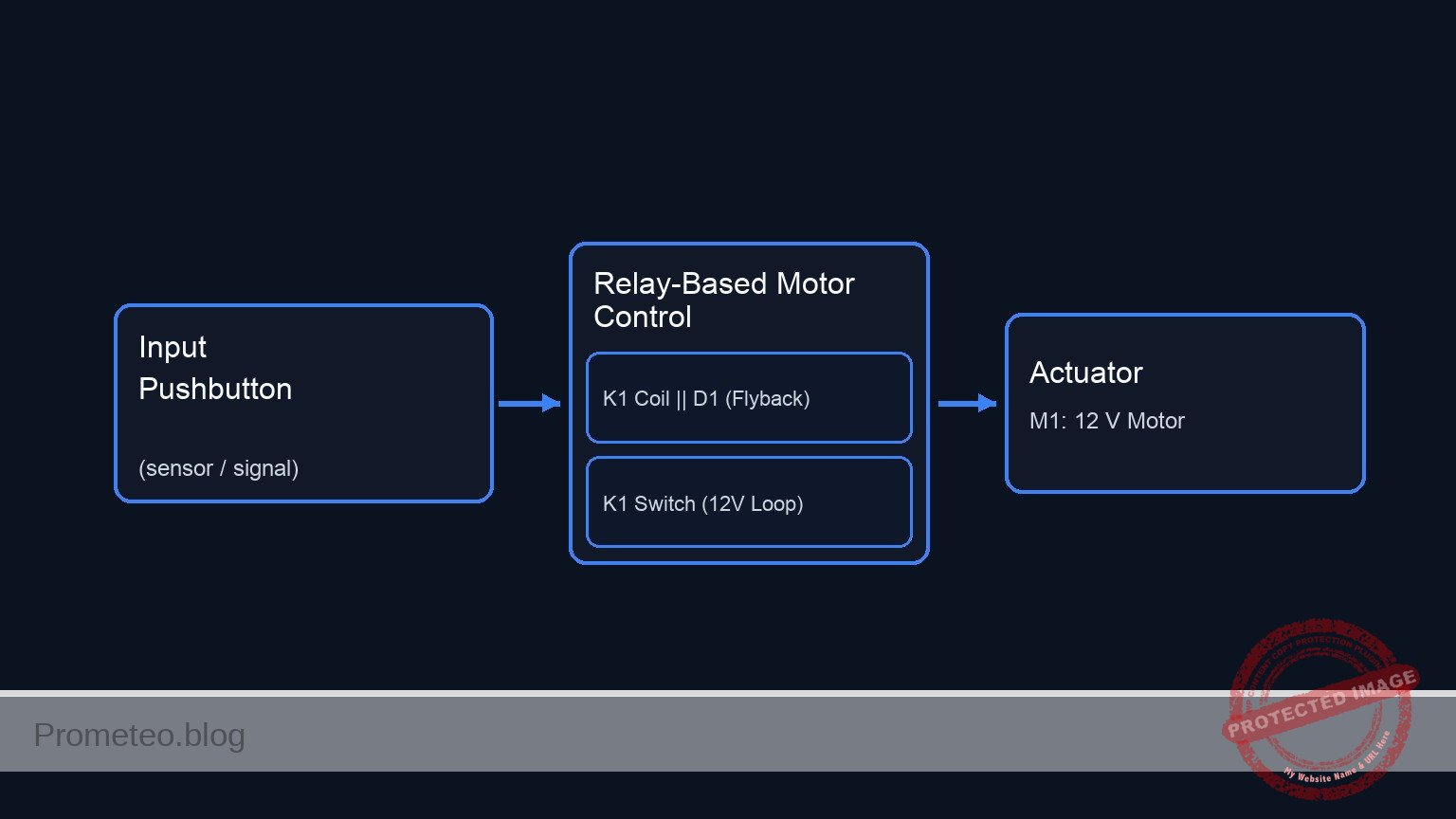
You will build a driver circuit that uses a small 5 V signal to activate an electromechanical relay, which in turn switches a separate 12 V high-power circuit powering a bulb.
-
Why it is useful:
- Automotive Systems: Allows a low-current ECU signal to switch high-current headlights.
- Safety: Keeps high voltage/current (the load side) physically separated from the sensitive control logic (the user side).
- Interface: Enables microcontrollers (like Arduino/ESP32) to control industrial equipment or AC appliances (simulated here with 12 V).
-
Expected outcome:
- The 12 V bulb turns ON only when the 5 V control switch is closed.
- An audible «click» is heard from the relay component when switching states.
- Measurements: 0 V on the load when the control signal is 0 V; ~12 V on the load when the control signal is 5 V.
-
Target audience: Students dealing with electromechanical interfaces and circuit protection.
Materials
- V1: 5 V DC voltage source, function: Control Logic Supply
- V2: 12 V DC voltage source, function: High Power Load Supply
- S1: SPST Toggle Switch, function: Control trigger
- R1: 1 kΩ resistor, function: Base current limiter for Q1
- Q1: 2N2222 NPN BJT Transistor, function: Relay coil driver
- D1: 1N4007 Diode, function: Flyback protection (snubber)
- K1: 5 V SPST Relay (coil resistance ~70 Ω), function: Galvanic isolation switch
- L1: 12 V / 10 W Incandescent Bulb, function: High power load
Wiring guide
This guide uses specific node names to ensure correct connections in simulation and assembly. The circuit has two isolated sides: the Control Side (Nodes: V_CTRL, 0) and the Load Side (Nodes: V_HV, GND_LOAD).
Control Side (Low Power):
* V1 (+): Connects to Node V_CTRL.
* V1 (-): Connects to Node 0 (Common Ground).
* S1: Connects between V_CTRL and Node V_TRIG.
* R1: Connects between V_TRIG and Node V_BASE.
* Q1 (Base): Connects to Node V_BASE.
* Q1 (Emitter): Connects to Node 0.
* Q1 (Collector): Connects to Node COIL_LOW.
* K1 (Coil pin 1): Connects to Node V_CTRL.
* K1 (Coil pin 2): Connects to Node COIL_LOW.
* D1 (Anode): Connects to Node COIL_LOW.
* D1 (Cathode): Connects to Node V_CTRL (Reverse biased across coil).
Load Side (High Power):
* V2 (+): Connects to Node V_HV.
* V2 (-): Connects to Node GND_LOAD (Isolated from Node 0).
* K1 (Common Contact): Connects to Node V_HV.
* K1 (Normally Open Contact): Connects to Node BULB_IN.
* L1: Connects between Node BULB_IN and Node GND_LOAD.
Conceptual block diagram
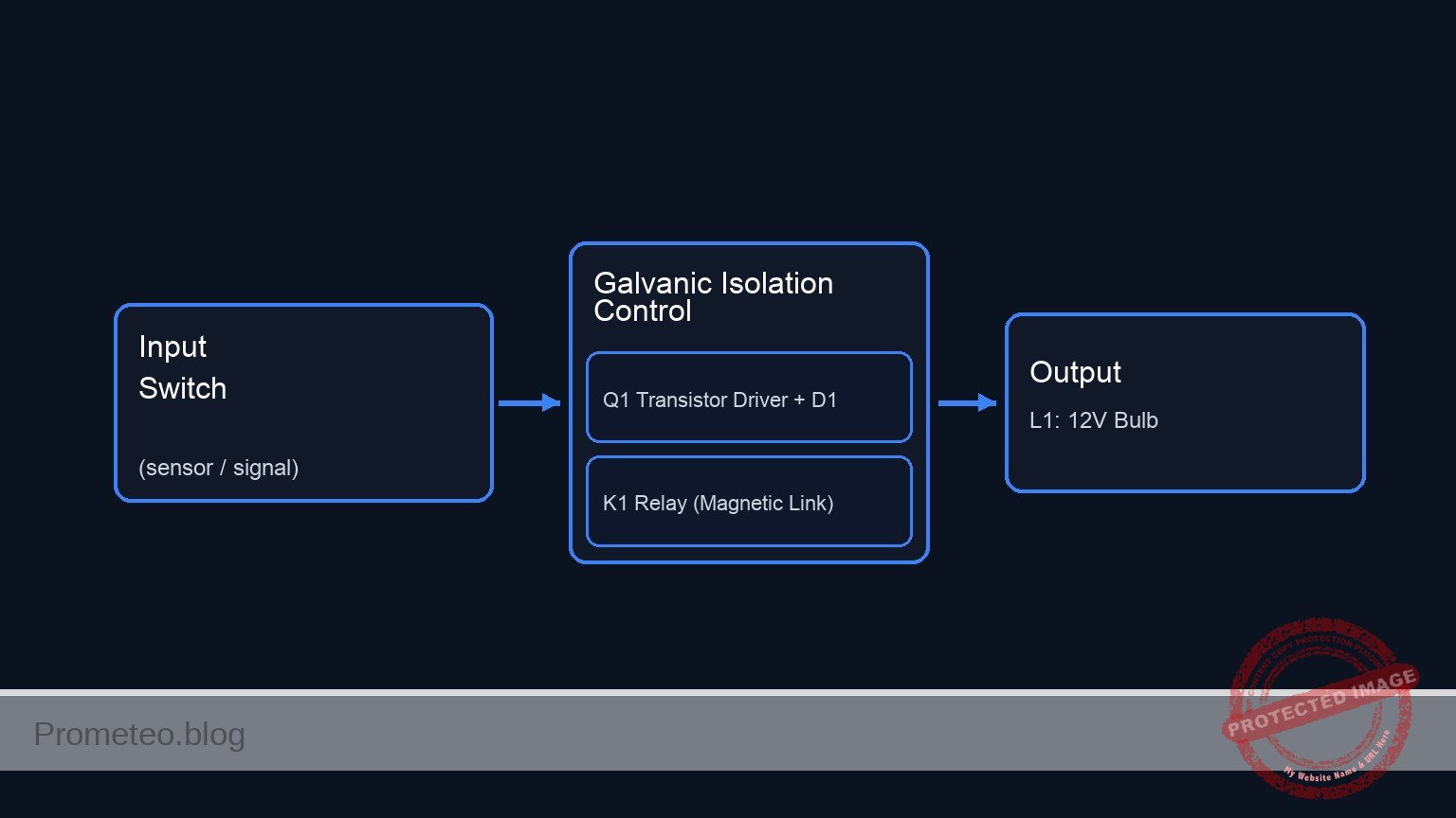
Schematic
+-------------------------------------------------------------------------+
|               PRACTICAL CASE: HIGH POWER CIRCUIT ISOLATION              |
+-------------------------------------------------------------------------+

===========================================================================
  PART 1: CONTROL SIDE (5 V Logic)
  Nodes: V_CTRL, V_TRIG, V_BASE, COIL_LOW, 0 (GND)
===========================================================================

  (Trigger Signal Path)
  [ V1: 5 V (+) ] --> [ S1: Switch ] --> [ R1: 1k Ohm ] --> [ Q1: Base ]
                                                               |
                                                               | (Controls)
                                                               v
  (Coil Power Path)                                    [ Q1: Collector ]
  [ V1: 5 V (+) ] ---------> [ K1: Relay Coil ] --------------> |
                            [ || D1 Diode    ]                 |
                            [ (Rev Biased)   ]                 | (Conducts to)
                                                               |
                                                               v
                                                       [ Q1: Emitter ]
                                                               |
                                                               v
                                                       [ Node 0 (GND) ]


             ~ ~ ~ ~ ~ ~ ~ ~ ~ ~ ~ ~ ~ ~ ~ ~ ~ ~ ~ ~ ~ ~ ~
             ~      MAGNETIC LINK (GALVANIC ISOLATION)   ~
             ~ ~ ~ ~ ~ ~ ~ ~ ~ ~ ~ ~ ~ ~ ~ ~ ~ ~ ~ ~ ~ ~ ~


===========================================================================
  PART 2: LOAD SIDE (12 V High Power)
  Nodes: V_HV, BULB_IN, GND_LOAD
===========================================================================

  (High Current Path)

  [ V2: 12 V (+) ] --> [ K1: Relay Switch ] --> [ L1: 12 V Bulb ] --> [ GND_LOAD ]
                      [   (COM -> NO)    ]
Measurements and tests
Follow these steps to validate the isolation and switching capability:
-
Coil Voltage Test:
- Close switch S1.
- Measure voltage between
V_CTRLandCOIL_LOW. - Result: It should read approximately 5 V (indicating the transistor is sinking current).
-
Load Activation:
- Keep S1 closed.
- Observe L1 (Bulb).
- Result: The bulb illuminates. Measure voltage across L1; it should be ~12 V.
-
Switch Latency (Oscilloscope required):
- Connect Channel 1 to
V_TRIGand Channel 2 toBULB_IN. - Toggle S1 from OFF to ON.
- Result: You will observe a delay (typically 5–15 ms) between the signal rising on Ch1 and power appearing on Ch2. This is the mechanical switching time of the relay armature.
- Connect Channel 1 to
SPICE netlist and simulation
Reference SPICE Netlist (ngspice) — excerptFull SPICE netlist (ngspice)
* High power circuit isolation
*
* This netlist simulates a relay driver circuit with a high-power load.
* It includes a low-voltage control side (5V) and an isolated high-voltage load side (12V).
*

* --- Analysis Setup ---
.tran 10u 10m
.print tran V(V_TRIG) V(BULB_IN) V(COIL_LOW) I(L_K1_COIL)

* --- Control Side (Low Power) ---

* Supply V1: 5V DC
V1 V_CTRL 0 DC 5

* Switch S1: Modeled as a Pulse Voltage Source to simulate user actuation
* Connects to V_TRIG to drive the base resistor.
* Timing: Off for 1ms, On for 4ms, then Off.
V_S1 V_TRIG 0 PULSE(0 5 1m 10u 10u 4m 10m)

* ... (truncated in public view) ...
Copy this content into a .cir file and run with ngspice.
* High power circuit isolation
*
* This netlist simulates a relay driver circuit with a high-power load.
* It includes a low-voltage control side (5V) and an isolated high-voltage load side (12V).
*

* --- Analysis Setup ---
.tran 10u 10m
.print tran V(V_TRIG) V(BULB_IN) V(COIL_LOW) I(L_K1_COIL)

* --- Control Side (Low Power) ---

* Supply V1: 5V DC
V1 V_CTRL 0 DC 5

* Switch S1: Modeled as a Pulse Voltage Source to simulate user actuation
* Connects to V_TRIG to drive the base resistor.
* Timing: Off for 1ms, On for 4ms, then Off.
V_S1 V_TRIG 0 PULSE(0 5 1m 10u 10u 4m 10m)

* Resistor R1: 1k Base Current Limiter
R1 V_TRIG V_BASE 1k

* Transistor Q1: 2N2222 NPN Relay Driver
* Connections: Collector=COIL_LOW, Base=V_BASE, Emitter=0
Q1 COIL_LOW V_BASE 0 2N2222MOD

* Relay Coil K1 (Coil Side)
* Modeled as Inductance + Resistance in series between V_CTRL and COIL_LOW
R_K1_COIL V_CTRL INT_COIL 70
L_K1_COIL INT_COIL COIL_LOW 50m

* Diode D1: Flyback protection (Snubber)
* Anode=COIL_LOW, Cathode=V_CTRL
D1 COIL_LOW V_CTRL 1N4007MOD

* --- Load Side (High Power) ---

* Ground Isolation: High resistance path to global ground 0 to prevent singular matrix
R_ISO GND_LOAD 0 100Meg

* Supply V2: 12V DC
V2 V_HV GND_LOAD DC 12

* Relay Contact K1 (Switch Side)
* Modeled as a Voltage Controlled Switch
* Controlled by the voltage across the coil: V(V_CTRL) - V(COIL_LOW)
* Connects V_HV to BULB_IN when coil is energized
S_K1 V_HV BULB_IN V_CTRL COIL_LOW RELAY_SW_MOD

* Load L1: 12V / 10W Bulb
* Resistance ~ 14.4 Ohms (R = V^2 / P = 144 / 10)
R_L1 BULB_IN GND_LOAD 14.4

* --- Component Models ---

* NPN Transistor Model
.model 2N2222MOD NPN(IS=1E-14 VAF=100 BF=200 IKF=0.3 XTB=1.5 BR=3 CJC=8E-12 CJE=25E-12 TR=46.91E-9 TF=411.1E-12 ITF=0.6 VTF=1.7 XTF=3 RB=10 RC=0.3 RE=0.2)

* Diode Model
.model 1N4007MOD D(IS=7.02767n RS=0.0341512 N=1.80803 EG=1.11 XTI=3 BV=1000 IBV=5u CJO=10p VJ=0.7 M=0.5 FC=0.5 TT=100n)

* Relay Switch Model
* Threshold Vt=2.5V (Coil is 5V), Hysteresis Vh=0.5V
.model RELAY_SW_MOD SW(Vt=2.5 Vh=0.5 Ron=0.1 Roff=100Meg)

.op
.end
Simulation Results (Transient Analysis)

Show raw data table (4100 rows)
Index   time            v(v_trig)       v(bulb_in)      v(coil_low)     l_k1_coil#branc
0	0.000000e+00	0.000000e+00	1.722670e-06	5.000000e+00	1.002664e-11
1	1.000000e-07	0.000000e+00	1.722670e-06	5.000000e+00	1.002626e-11
2	2.000000e-07	0.000000e+00	1.722670e-06	5.000000e+00	1.002547e-11
3	4.000000e-07	0.000000e+00	1.722670e-06	5.000000e+00	1.002342e-11
4	8.000000e-07	0.000000e+00	1.722670e-06	5.000000e+00	1.001814e-11
5	1.600000e-06	0.000000e+00	1.722670e-06	5.000000e+00	1.000316e-11
6	3.200000e-06	0.000000e+00	1.722670e-06	5.000000e+00	9.969744e-12
7	6.400000e-06	0.000000e+00	1.722670e-06	5.000000e+00	1.000801e-11
8	1.280000e-05	0.000000e+00	1.722670e-06	5.000000e+00	1.002921e-11
9	2.280000e-05	0.000000e+00	1.722670e-06	5.000000e+00	9.970357e-12
10	3.280000e-05	0.000000e+00	1.722670e-06	5.000000e+00	1.004993e-11
11	4.280000e-05	0.000000e+00	1.722670e-06	5.000000e+00	9.955463e-12
12	5.280000e-05	0.000000e+00	1.722670e-06	5.000000e+00	1.004077e-11
13	6.280000e-05	0.000000e+00	1.722670e-06	5.000000e+00	9.984500e-12
14	7.280000e-05	0.000000e+00	1.722670e-06	5.000000e+00	1.001134e-11
15	8.280000e-05	0.000000e+00	1.722670e-06	5.000000e+00	1.001578e-11
16	9.280000e-05	0.000000e+00	1.722670e-06	5.000000e+00	1.000519e-11
17	1.028000e-04	0.000000e+00	1.722670e-06	5.000000e+00	1.003686e-11
18	1.128000e-04	0.000000e+00	1.722670e-06	5.000000e+00	9.961732e-12
19	1.228000e-04	0.000000e+00	1.722670e-06	5.000000e+00	1.005266e-11
20	1.328000e-04	0.000000e+00	1.722670e-06	5.000000e+00	9.963169e-12
21	1.428000e-04	0.000000e+00	1.722670e-06	5.000000e+00	1.003205e-11
22	1.528000e-04	0.000000e+00	1.722670e-06	5.000000e+00	9.984436e-12
23	1.628000e-04	0.000000e+00	1.722670e-06	5.000000e+00	1.001919e-11
... (4076 more rows) ...
Common mistakes and how to avoid them
-
Omitting the flyback diode (D1):
- Error: The transistor Q1 fails permanently after a few switches.
- Solution: Always place a diode in reverse bias parallel to the relay coil to absorb the high-voltage spike generated when the magnetic field collapses.
-
Sharing Grounds unintentionally:
- Error: Connecting
GND_LOADto Node0on the breadboard. - Solution: While the circuit will work, you lose galvanic isolation. Keep the high-power return path physically separate from the logic ground.
- Error: Connecting
-
Insufficient Base Current:
- Error: Using a resistor R1 that is too high (e.g., 100 kΩ). The relay does not click or clicks weakly.
- Solution: Ensure the transistor is in saturation. For a 2N2222 driving a standard relay, 1 kΩ is usually sufficient.
Troubleshooting
-
Symptom: Relay clicks, but the bulb does not light up.
- Cause: Issue on the Load Side (Secondary circuit).
- Fix: Check V2 supply, verify the bulb L1 is not burnt, and ensure connections to the Relay COM/NO pins are tight.
-
Symptom: No sound from relay, Bulb OFF.
- Cause: The coil is not energizing.
- Fix: Check voltage at Node
V_BASE. If 0 V, check S1. If ~0.7 V, check if Q1 is installed correctly (E-B-C pinout).
-
Symptom: Transistor gets extremely hot.
- Cause: Coil current is too high for the selected transistor.
- Fix: Verify the relay coil resistance. If it draws >600 mA, the 2N2222 might be underpowered; use a power transistor (e.g., TIP31) or a MOSFET.
Possible improvements and extensions
- Status Indicator: Add a small LED and a 330 Ω resistor in parallel with the Relay Coil to visually indicate when the control signal is active.
- Solid State Upgrade: Replace the mechanical relay (K1) and transistor driver with an Optocoupler and a MOSFET (or Triac for AC) to eliminate mechanical wear and reduce switching latency.
More Practical Cases on Prometeo.blog
Find this product and/or books on this topic on Amazon
As an Amazon Associate, I earn from qualifying purchases. If you buy through this link, you help keep this project running.
Quick Quiz

Telecommunications Electronics Engineer and Computer Engineer (official degrees in Spain).