Level: Basic. Build a circuit to amplify a weak audio signal using an NPN transistor in common-emitter configuration.
Objective and use case
In this case, you will build a classic single-stage Class A amplifier using an NPN transistor with voltage divider biasing. You will input a small AC signal (representing audio) and observe a larger voltage swing at the output.
-
Why it is useful:
- Pre-amplification: Boosts weak signals from microphones before they reach a power amplifier.
- Signal conditioning: Raises sensor output levels to be readable by microcontrollers.
- Analog processing: Fundamental building block for filters, oscillators, and mixers.
- Impedance matching: Buffers high-impedance sources to drive lower-impedance loads (depending on specific configuration).
-
Expected outcome:
- DC Operating Point: VCE stabilizes around half the supply voltage (VCC / 2) for maximum swing.
- Amplification: The AC output voltage (Vout) is significantly larger than the input (Vin), indicating Voltage Gain (Av > 1).
- Phase Inversion: The output signal waveform is inverted (180^\circ) relative to the input.
- Current Flow: IC is controlled by IB according to the transistor’s beta (\beta).
-
Target audience and level: Students with basic knowledge of Ohm’s Law and component identification.
Materials
- V1: 9 V DC battery or bench supply, function: main circuit power.
- V2: Signal Generator (Sine wave, 1 kHz, 20 mV peak-to-peak), function: simulates weak audio input.
- Q1: 2N3904 (or 2N2222) NPN BJT, function: active amplifying element.
- R1: 22 kΩ resistor, function: upper base bias divider.
- R2: 6.8 kΩ resistor, function: lower base bias divider.
- R3: 4.7 kΩ resistor, function: collector load (sets gain and output impedance).
- R4: 1 kΩ resistor, function: emitter degeneration (sets DC stability).
- C1: 10 µF electrolytic capacitor, function: input DC blocking.
- C2: 10 µF electrolytic capacitor, function: output DC blocking.
- C3: 100 µF electrolytic capacitor, function: emitter bypass (increases AC gain).
Wiring guide
Use the following nodes to wire your circuit: VCC (9 V), 0 (GND), BASE, COLL, EMIT, VIN, VOUT.
- V1: Positive terminal connects to
VCC, Negative terminal connects to0. - V2: Signal output connects to
VIN, Ground connects to0. - R1: Connects between
VCCandBASE. - R2: Connects between
BASEand0. - R3: Connects between
VCCandCOLL. - R4: Connects between
EMITand0. - Q1: Collector pin to
COLL, Base pin toBASE, Emitter pin toEMIT. - C1: Positive leg to
BASE, Negative leg toVIN. - C2: Positive leg to
COLL, Negative leg toVOUT(Load/Scope probe connects here). - C3: Positive leg to
EMIT, Negative leg to0(Place in parallel with R4).
Conceptual block diagram
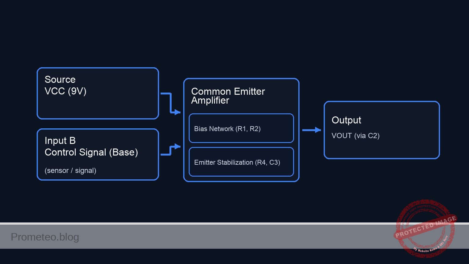
Schematic
Title: Practical case: Simple audio amplifier

      (BIAS & INPUT NETWORK)                               (POWER & OUTPUT NETWORK)
      ======================                               ========================

                                                           VCC (9 V)
      VCC (9 V)                                                |
         |                                                    |
         v                                                    v
    [ R1: 22k ]                                          [ R3: 4.7k ]
         |                                                    |
         v                                                    v
      (BASE) --------(Control Signal)----------------> [ Q1: Collector ] <--(COLL)--+
         ^                                                    |                     |
         |                                                    | (Amplified Current) |
    [ C1: 10uF ] <--(VIN)-- [ V2: Source ]                    v                     |
         |                                             [ Q1: Emitter ]              +--> [ C2: 10uF ] --> VOUT
         v                                                    |
    [ R2: 6.8k ]                                              v
         |                                                  (EMIT)
         v                                                    |
        GND                                       +-----------+-----------+
                                                  |                       |
                                                  v                       v
                                             [ R4: 1k ]             [ C3: 100uF ]
                                                  |                       |
                                                  v                       v
                                                 GND                     GND
Measurements and tests
Perform these tests using a Multimeter (DMM) and an Oscilloscope (if available).
-
DC Bias Check (Quiescent Point):
- Ensure V2 (AC source) is OFF or disconnected.
- Measure voltage from
COLLto0. It should be approximately 4 V to 5 V (roughly half ofVCC). - Measure voltage from
EMITto0. It should be approximately 1 V (VE). - Measure voltage from
BASEtoEMIT(VBE). It must be ~0.65 V to 0.7 V for the transistor to be active.
-
Current Calculation:
- Calculate Collector Current (IC): IC ≈ VEMIT / R4. Expect approx 1 mA.
- Calculate Base Current (IB): IC / \beta (assuming \beta ≈ 100, IB ≈ 10 µ A).
-
AC Gain Verification:
- Connect V2 (
VIN) with a 20 mV peak-to-peak sine wave at 1 kHz. - Measure the Peak-to-Peak voltage at
VOUT. - Calculate Voltage Gain (Av): Av = Voutpp / Vinpp.
- Observation: Without C3, gain is low (≈ R3 / R4). With C3 connected, gain should increase significantly.
- Connect V2 (
SPICE netlist and simulation
Reference SPICE Netlist (ngspice) — excerptFull SPICE netlist (ngspice)
* Practical case: Simple audio amplifier

* --- Power Supply ---
* V1: 9 V DC battery
V1 VCC 0 DC 9

* --- Input Signal ---
* V2: Signal Generator (Sine wave, 1 kHz, 20 mV peak-to-peak -> 10mV Amplitude)
V2 VIN 0 SIN(0 10m 1k)

* --- Components ---
* Q1: 2N3904 NPN BJT
Q1 COLL BASE EMIT 2N3904

* R1: Upper base bias divider
R1 VCC BASE 22k

* R2: Lower base bias divider
R2 BASE 0 6.8k

* ... (truncated in public view) ...
Copy this content into a .cir file and run with ngspice.
* Practical case: Simple audio amplifier

* --- Power Supply ---
* V1: 9 V DC battery
V1 VCC 0 DC 9

* --- Input Signal ---
* V2: Signal Generator (Sine wave, 1 kHz, 20 mV peak-to-peak -> 10mV Amplitude)
V2 VIN 0 SIN(0 10m 1k)

* --- Components ---
* Q1: 2N3904 NPN BJT
Q1 COLL BASE EMIT 2N3904

* R1: Upper base bias divider
R1 VCC BASE 22k

* R2: Lower base bias divider
R2 BASE 0 6.8k

* R3: Collector load
R3 VCC COLL 4.7k

* R4: Emitter degeneration
R4 EMIT 0 1k

* C1: Input DC blocking (Positive leg to BASE, Negative leg to VIN)
C1 BASE VIN 10u

* C2: Output DC blocking (Positive leg to COLL, Negative leg to VOUT)
C2 COLL VOUT 10u

* C3: Emitter bypass (Positive leg to EMIT, Negative leg to 0)
C3 EMIT 0 100u

* --- Load Simulation ---
* High impedance load to simulate scope probe and prevent floating node error at VOUT
R_SCOPE VOUT 0 1Meg

* --- Models ---
.model 2N3904 NPN(IS=1E-14 VAF=100 BF=300 IKF=0.4 XTB=1.5 BR=4 CJC=4E-12 CJE=8E-12 RB=20 RC=0.1 RE=0.1 TR=250n TF=350p ITF=1 VTF=2 XTF=3)

* --- Analysis Directives ---
.op
.tran 10u 5ms

* --- Output ---
* Prints Input and Output voltages, plus internal transistor nodes
.print tran V(VIN) V(VOUT) V(BASE) V(COLL) V(EMIT)

.end
Simulation Results (Transient Analysis)

Show raw data table (511 rows)
Index   time            v(vin)          v(vout)         v(base)         v(coll)         v(emit)
0	0.000000e+00	0.000000e+00	0.000000e+00	2.100182e+00	2.275541e+00	1.435514e+00
1	1.000000e-07	6.283185e-06	-1.11372e-03	2.100188e+00	2.274427e+00	1.435514e+00
2	2.000000e-07	1.256637e-05	-2.51792e-03	2.100195e+00	2.273023e+00	1.435514e+00
3	4.000000e-07	2.513271e-05	-5.47602e-03	2.100207e+00	2.270065e+00	1.435514e+00
4	8.000000e-07	5.026527e-05	-1.15278e-02	2.100232e+00	2.264013e+00	1.435514e+00
5	1.600000e-06	1.005293e-04	-2.35622e-02	2.100283e+00	2.251979e+00	1.435514e+00
6	3.200000e-06	2.010484e-04	-4.77358e-02	2.100383e+00	2.227805e+00	1.435514e+00
7	6.400000e-06	4.020155e-04	-9.61836e-02	2.100584e+00	2.179357e+00	1.435514e+00
8	1.280000e-05	8.033810e-04	-1.93689e-01	2.100985e+00	2.081852e+00	1.435516e+00
9	2.280000e-05	1.427671e-03	-3.47124e-01	2.101609e+00	1.928416e+00	1.435522e+00
10	3.280000e-05	2.046327e-03	-5.01331e-01	2.102227e+00	1.774210e+00	1.435531e+00
11	4.280000e-05	2.656907e-03	-6.48595e-01	2.102836e+00	1.626945e+00	1.435544e+00
12	5.280000e-05	3.257002e-03	-7.15494e-01	2.103433e+00	1.560045e+00	1.435558e+00
13	6.280000e-05	3.844242e-03	-7.38189e-01	2.104013e+00	1.537349e+00	1.435575e+00
14	7.280000e-05	4.416311e-03	-7.50146e-01	2.104572e+00	1.525391e+00	1.435592e+00
15	8.280000e-05	4.970951e-03	-7.58389e-01	2.105109e+00	1.517147e+00	1.435610e+00
16	9.280000e-05	5.505973e-03	-7.63991e-01	2.105621e+00	1.511545e+00	1.435628e+00
17	1.028000e-04	6.019265e-03	-7.68326e-01	2.106106e+00	1.507209e+00	1.435647e+00
18	1.128000e-04	6.508802e-03	-7.71816e-01	2.106563e+00	1.503719e+00	1.435667e+00
19	1.228000e-04	6.972652e-03	-7.74681e-01	2.106990e+00	1.500853e+00	1.435687e+00
20	1.328000e-04	7.408984e-03	-7.77018e-01	2.107384e+00	1.498515e+00	1.435707e+00
21	1.428000e-04	7.816076e-03	-7.78966e-01	2.107746e+00	1.496566e+00	1.435728e+00
22	1.528000e-04	8.192321e-03	-7.80567e-01	2.108073e+00	1.494964e+00	1.435750e+00
23	1.628000e-04	8.536235e-03	-7.81896e-01	2.108365e+00	1.493635e+00	1.435772e+00
... (487 more rows) ...
Common mistakes and how to avoid them
- Transistor Pinout Reversal: Swapping the Collector and Emitter prevents amplification and acts like a reverse-biased diode.
- Solution: Double-check the datasheet for the 2N3904 (E-B-C flat side facing you) before inserting.
- Capacitor Polarity: Electrolytic capacitors (C1, C2, C3) explode or fail if biased backwards.
- Solution: Ensure the positive lead (longer leg) faces the more positive DC potential (towards the transistor base/collector).
- Saturation or Cutoff: Using wrong resistor values shifts the Q-point, causing the signal to clip (flatten) immediately.
- Solution: Verify DC voltages at the Collector before applying an AC signal. If VC is near 9 V or 0 V, check R1 and R2.
Troubleshooting
- Symptom: No Output Signal.
- Cause: Loose connection, blown transistor, or V1 is off.
- Fix: Check continuity on the breadboard rails; verify V1 is 9 V.
- Symptom: Output is Clipped (Flat tops or bottoms).
- Cause: The amplifier is driven into saturation (flat bottom) or cutoff (flat top), or input signal is too large.
- Fix: Reduce input amplitude (V2); check bias resistors (R1, R2) to center the Q-point.
- Symptom: Low Gain (Output ≈ Input).
- Cause: Bypass capacitor C3 is missing, loose, or too small.
- Fix: Ensure C3 is connected solidly in parallel with R4. This shorts the emitter resistor for AC signals, maximizing gain.
Possible improvements and extensions
- Volume Control: Replace R2 (or add a pot before C1) with a 10 kΩ potentiometer to attenuate the input signal.
- Increased Power: Add a second transistor stage (Emitter Follower / Class B push-pull) after
VOUTto drive a small 8 Ω speaker instead of just observing voltage on a scope.
More Practical Cases on Prometeo.blog
Find this product and/or books on this topic on Amazon
As an Amazon Associate, I earn from qualifying purchases. If you buy through this link, you help keep this project running.
Quick Quiz

Telecommunications Electronics Engineer and Computer Engineer (official degrees in Spain).