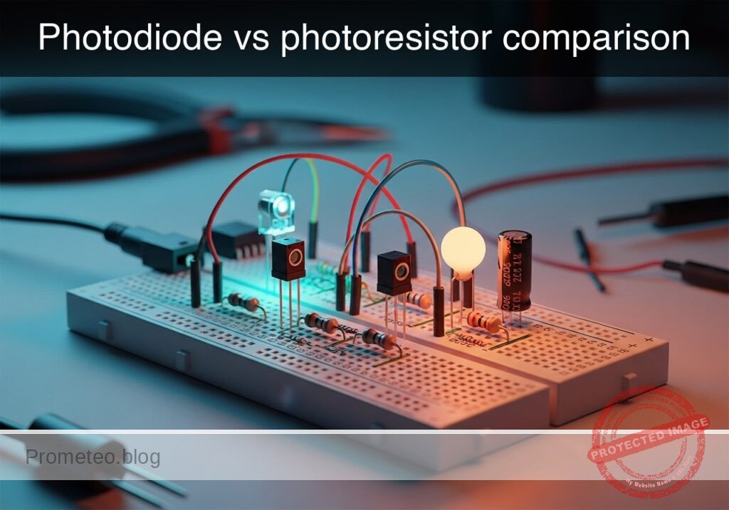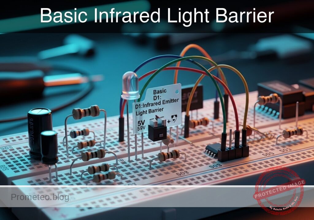
Level: Basic. Build a simple alarm system that detects the interruption of a light beam.
Objective and use case
In this project, you will build an optical detector system consisting of a transmitter (IR LED) and a receiver (Photodiode) that controls a transistor switch. When the invisible infrared beam is interrupted by an object, an alarm LED will light up.
- Security systems: Used in door or window frames to detect unauthorized entry.
- Automation: detecting objects on a conveyor belt for counting or sorting.
- Safety: Emergency stop mechanisms when a hand crosses a dangerous boundary.
- Touchless switching: Activating devices without physical contact.
Expected outcome:
* Beam Intact (Clear path): The Red Alarm LED is OFF.
* Beam Interrupted (Object present): The Red Alarm LED turns ON.
* Signal: The voltage at the sensing node will transition from Logic Low (approx. 0.1 V – 0.5 V) to Logic High (> 0.7 V) when the beam is broken.
* Target audience: Beginners familiar with breadboarding and basic discrete components.
Materials
- V1: 5 V DC supply
- D1: IR LED (Infrared Emitter), function: Beam transmitter (Tx)
- R1: 220 Ω resistor, function: Current limiting for D1
- D2: Photodiode, function: Beam receiver (Rx)
- R2: 100 kΩ resistor, function: Pull-up resistor for the sensing node
- Q1: 2N2222 (or 2N3904) NPN Transistor, function: Electronic switch
- R3: 1 kΩ resistor, function: Base current limiter for Q1
- D3: Red LED, function: Alarm indicator
- R4: 330 Ω resistor, function: Current limiting for D3
Wiring guide
This circuit is divided into two parts: the Transmitter (Tx) and the Receiver (Rx). Construct them facing each other.
Transmitter (Tx):
* VCC connects to R1.
* R1 connects to the Anode of D1 (Node: TX_ANODE).
* D1 (Cathode) connects to 0 (GND).
Receiver (Rx) – Dark Detector Configuration:
* VCC connects to R2.
* R2 connects to the Cathode of D2 (Node: V_SENSE). Note: Photodiodes are used in reverse bias.
* D2 (Anode) connects to 0 (GND).
* VCC connects to R4.
* R4 connects to the Anode of D3.
* D3 (Cathode) connects to the Collector of Q1 (Node: V_ALARM).
* Q1 (Emitter) connects to 0 (GND).
* Node V_SENSE connects to R3.
* R3 connects to the Base of Q1.
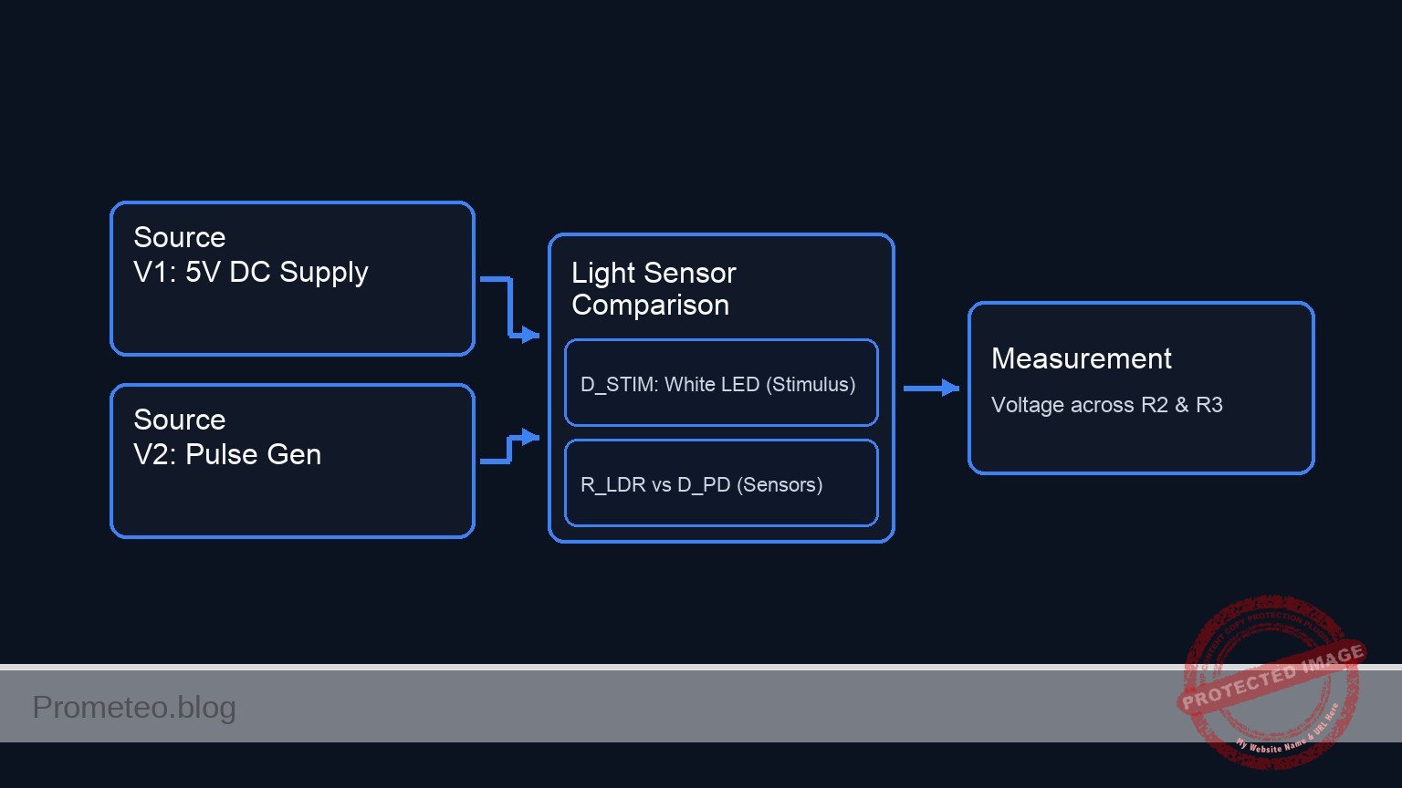
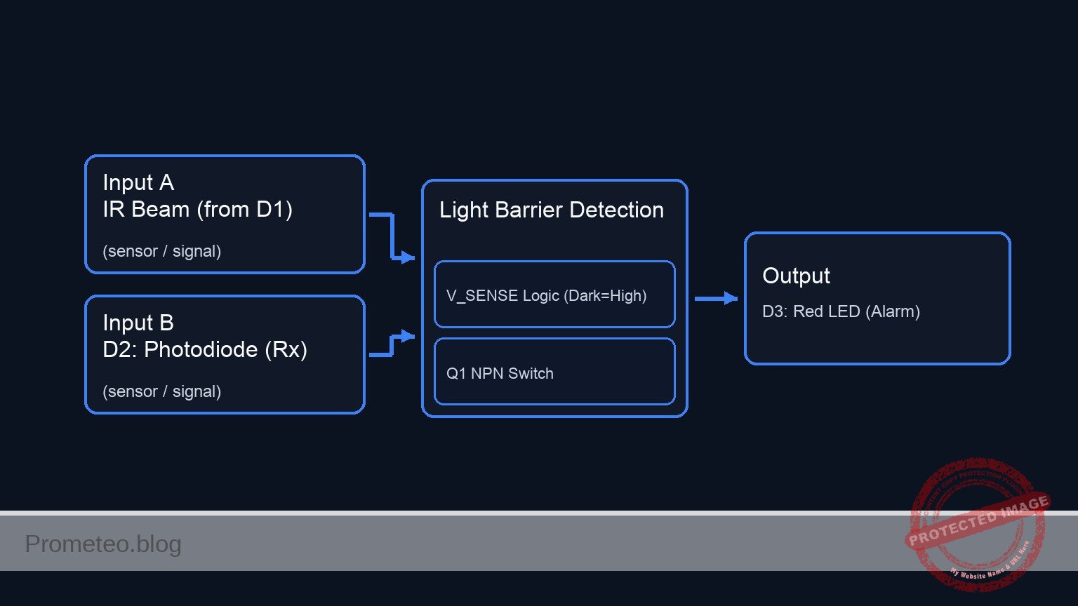
Conceptual block diagram
Schematic
+------------------------------------------------------------------------------+
|                   PRACTICAL CASE: BASIC INFRARED LIGHT BARRIER               |
+------------------------------------------------------------------------------+

      [ INPUTS / SENSORS ]              [ LOGIC / CONTROL ]               [ OUTPUT / LOAD ]

      (Transmitter)
      [ VCC ]
         |
         v
      [ R1: 220 ]
         |
         v
      [ D1: IR LED ] ~~~~~(IR Beam)~~~~~> [ D2: Photodiode ]
         |                                (Rx Sensor)
         v                                      |
      [ GND ]                                   |
                                                |
      (Receiver Bias)                           |
      [ VCC ]                                   |
         |                                      |
         v                                      |
      [ R2: 100k ]                              |
         |                                      |
         +-----------(Node: V_SENSE)------------+
         |
         |
         v
      [ R3: 1k ]
         |
         v
      [ Q1: NPN Base ] ----------------> [ Q1: Collector ] <--(Switched Path)-- [ D3: Red LED ]
      (Transistor Switch)                (Sinks Current)                              ^
                                                |                                     |
                                                v                                [ R4: 330 ]
                                         [ Q1: Emitter ]                              ^
                                                |                                     |
                                                v                                  [ VCC ]
                                             [ GND ]

+------------------------------------------------------------------------------+
| SIGNAL FLOW ANALYSIS:                                                        |
| 1. Tx generates IR Beam.                                                     |
| 2. If Beam hits D2 (Clear) -> D2 conducts -> V_SENSE is LOW -> Q1 OFF.       |
| 3. If Beam blocked (Dark)  -> D2 blocks   -> V_SENSE is HIGH -> Q1 ON.       |
| 4. Q1 ON connects D3 to GND -> ALARM ACTIVATED.                              |
+------------------------------------------------------------------------------+
System Logic Table
| Physical State | IR Beam Status | Photodiode (D2) Mode | V_SENSE Voltage | Transistor (Q1) | Alarm LED (D3) |
|---|---|---|---|---|---|
| Normal | Reaching Rx | Conducting (Low Resistance) | Low (< 0.6 V) | OFF (Cut-off) | OFF |
| Intrusion | Blocked/Broken | Blocking (High Impedance) | High (~VCC) | ON (Saturation) | ON |
Measurements and tests
- Tx Verification: Connect power. Use a smartphone camera to look at the IR LED (D1). You should see a faint purple/pink glow on the screen (human eyes cannot see IR).
- Rx Voltage Test (Beam Intact): Align D1 and D2 perfectly. Measure voltage at
V_SENSErelative to GND. It should be low (typically < 0.6 V) because the light causes the photodiode to conduct current to the ground. - Rx Voltage Test (Beam Broken): Place a card or your hand between D1 and D2. Measure voltage at
V_SENSE. It should rise significantly (close to 4 V–5 V) as the photodiode stops conducting and R2 pulls the node high. - Functional Test: Ensure the Red LED (D3) turns ON immediately when the beam is blocked and turns OFF when the path is clear.
SPICE netlist and simulation
Reference SPICE Netlist (ngspice) — excerptFull SPICE netlist (ngspice)
* Practical case: Basic Infrared Light Barrier

* --- Component Models ---
* Standard NPN Transistor
.model 2N2222 NPN (IS=1E-14 BF=200 VAF=100)
* Infrared LED (Tx) - Approx Vf=1.2V
.model IR_LED D (IS=1p N=1.5 RS=5)
* Red LED (Alarm) - Approx Vf=1.8-2.0V
.model RED_LED D (IS=1u N=2 RS=10)
* Photodiode (Rx) - Modeled as diode with low capacitance
.model PD_DIODE D (IS=10p N=1 RS=10 CJO=10p)

* --- Power Supply ---
V1 VCC 0 DC 5

* --- Transmitter (Tx) Circuit ---
* Connectivity: VCC -> R1 -> D1(Anode). D1(Cathode) -> GND.
R1 VCC TX_ANODE 220
D1 TX_ANODE 0 IR_LED

* ... (truncated in public view) ...
Copy this content into a .cir file and run with ngspice.
* Practical case: Basic Infrared Light Barrier

* --- Component Models ---
* Standard NPN Transistor
.model 2N2222 NPN (IS=1E-14 BF=200 VAF=100)
* Infrared LED (Tx) - Approx Vf=1.2V
.model IR_LED D (IS=1p N=1.5 RS=5)
* Red LED (Alarm) - Approx Vf=1.8-2.0V
.model RED_LED D (IS=1u N=2 RS=10)
* Photodiode (Rx) - Modeled as diode with low capacitance
.model PD_DIODE D (IS=10p N=1 RS=10 CJO=10p)

* --- Power Supply ---
V1 VCC 0 DC 5

* --- Transmitter (Tx) Circuit ---
* Connectivity: VCC -> R1 -> D1(Anode). D1(Cathode) -> GND.
R1 VCC TX_ANODE 220
D1 TX_ANODE 0 IR_LED

* --- Receiver (Rx) Circuit ---
* Sensor Stage: VCC -> R2 -> D2(Cathode). D2(Anode) -> GND.
* Node V_SENSE is the junction of R2 and D2.
R2 VCC V_SENSE 100k
D2 0 V_SENSE PD_DIODE

* PHYSICAL STIMULUS: IR Beam Simulation
* In a real circuit, D1 emits light which D2 receives.
* We model this optical coupling with a Current Source (Photocurrent) in parallel with D2.
* Direction: Photocurrent flows Cathode to Anode (V_SENSE to GND).
* Logic:
*   - 50uA = Light Detected (Beam Intact) -> V_SENSE pulled Low -> Alarm OFF.
*   - 0A   = Dark (Beam Broken) -> V_SENSE pulled High by R2 -> Alarm ON.
* Timing: Start with Light (50uA), break beam at 1ms (0A), restore at 3ms.
I_Beam V_SENSE 0 PULSE(50u 0 1m 10u 10u 2m 5m)

* Switch Stage: V_SENSE -> R3 -> Q1(Base)
R3 V_SENSE Q1_BASE 1k
* Q1: Collector=V_ALARM, Base=Q1_BASE, Emitter=GND
Q1 V_ALARM Q1_BASE 0 2N2222

* Alarm Indicator Stage: VCC -> R4 -> D3(Anode). D3(Cathode) -> Q1(Collector).
R4 VCC LED_ANODE 330
D3 LED_ANODE V_ALARM RED_LED

* --- Analysis Directives ---
* Transient analysis for 5ms to capture the beam break event
.tran 10u 5m

* Print required voltages for verification
.print tran V(V_SENSE) V(Q1_BASE) V(V_ALARM) V(TX_ANODE)

.op
.end
Simulation Results (Transient Analysis)

Show raw data table (1072 rows)
Index   time            v(v_sense)      v(q1_base)      v(v_alarm)
0	0.000000e+00	5.009804e-07	5.059904e-07	4.999999e+00
1	1.000000e-07	5.009804e-07	5.059904e-07	4.999999e+00
2	2.000000e-07	5.009804e-07	5.059904e-07	4.999999e+00
3	4.000000e-07	5.009804e-07	5.059904e-07	4.999999e+00
4	8.000000e-07	5.009804e-07	5.059904e-07	4.999999e+00
5	1.600000e-06	5.009804e-07	5.059904e-07	4.999999e+00
6	3.200000e-06	5.009804e-07	5.059904e-07	4.999999e+00
7	6.400000e-06	5.009804e-07	5.059904e-07	4.999999e+00
8	1.280000e-05	5.009804e-07	5.059904e-07	4.999999e+00
9	2.280000e-05	5.009804e-07	5.059904e-07	4.999999e+00
10	3.280000e-05	5.009804e-07	5.059904e-07	4.999999e+00
11	4.280000e-05	5.009804e-07	5.059904e-07	4.999999e+00
12	5.280000e-05	5.009804e-07	5.059904e-07	4.999999e+00
13	6.280000e-05	5.009804e-07	5.059904e-07	4.999999e+00
14	7.280000e-05	5.009804e-07	5.059904e-07	4.999999e+00
15	8.280000e-05	5.009804e-07	5.059904e-07	4.999999e+00
16	9.280000e-05	5.009804e-07	5.059904e-07	4.999999e+00
17	1.028000e-04	5.009804e-07	5.059904e-07	4.999999e+00
18	1.128000e-04	5.009804e-07	5.059904e-07	4.999999e+00
19	1.228000e-04	5.009804e-07	5.059904e-07	4.999999e+00
20	1.328000e-04	5.009804e-07	5.059904e-07	4.999999e+00
21	1.428000e-04	5.009804e-07	5.059904e-07	4.999999e+00
22	1.528000e-04	5.009804e-07	5.059904e-07	4.999999e+00
23	1.628000e-04	5.009804e-07	5.059904e-07	4.999999e+00
... (1048 more rows) ...
Common mistakes and how to avoid them
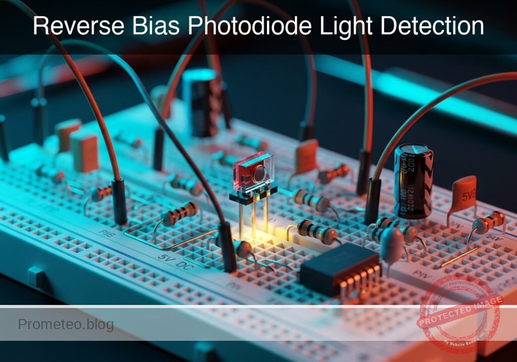
- Reversed Photodiode: Unlike regular LEDs, photodiodes must be connected in reverse bias (Cathode to positive side, Anode to negative side) to detect light. If connected forward, it acts like a normal diode and clamps the voltage, disabling the sensor.
- Misalignment: IR light is highly directional. If the Tx LED and Rx Photodiode are not pointing directly at each other, the alarm will stay ON permanently.
- Ambient Light Interference: Strong sunlight or overhead lamps can flood the photodiode, keeping the voltage low even when you block the IR beam. Use a small tube or black tape around the photodiode to shield it from side light.
Troubleshooting
- Alarm never turns ON:
- Cause: Transistor base not receiving enough voltage.
- Fix: Check if the object is truly blocking the light. Increase R2 (e.g., to 220 kΩ) to make the pull-up stronger against leakage.
- Alarm never turns OFF:
- Cause: Photodiode not receiving enough IR light to pull the base voltage down.
- Fix: Re-align the LEDs. Decrease R1 to make the IR LED brighter (do not go below 100 Ω). Ensure the photodiode is inserted with the correct polarity.
- System flickers:
- Cause: Edge detection or unstable light source.
- Fix: Ensure the power supply is stable. Add a small capacitor (e.g., 100 nF) between
V_SENSEand GND to filter noise (note: this slows response slightly).
Possible improvements and extensions
- Schmitt Trigger: Replace the simple transistor driver with a Schmitt Trigger (or 555 timer) to prevent the LED from fading in/out effectively creating a «snap» action switch.
- Modulation: Use a 38 kHz receiver module (like a TSOP sensor) and pulse the IR LED at 38 kHz. This makes the system completely immune to sunlight and room lighting.
More Practical Cases on Prometeo.blog
Find this product and/or books on this topic on Amazon
As an Amazon Associate, I earn from qualifying purchases. If you buy through this link, you help keep this project running.
Quick Quiz

Telecommunications Electronics Engineer and Computer Engineer (official degrees in Spain).