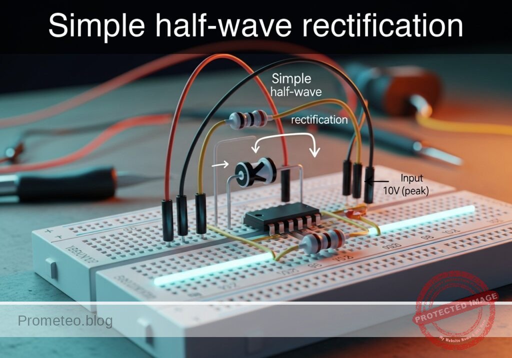
Level: Basic. Visualizing how a diode converts AC to pulsating DC by removing the negative half-cycle.
Objective and use case
You will build a fundamental analog circuit that uses a single semiconductor diode to block the negative portion of an alternating current (AC) signal, passing only the positive portion to a resistive load.
Why it is useful:
* Power conversion: It represents the first stage in converting AC mains power to DC for electronic devices.
* Signal demodulation: Used in AM radios to extract audio signals from radio frequency carriers (envelope detector).
* Polarity protection: Similar logic prevents damage to DC circuits if batteries are inserted backward.
Expected outcome:
* Input Signal: A complete sine wave swinging between positive and negative voltages (e.g., +10 V to -10 V).
* Output Signal: A pulsating waveform showing only the positive «humps» of the sine wave; the voltage sits at 0 V during the negative cycle.
* Voltage Drop: The peak output voltage will be approximately 0.7 V lower than the input peak due to the silicon diode forward voltage drop.
* Frequency: The output frequency remains identical to the input frequency.
Target audience and level: Students and hobbyists learning basic analog components.
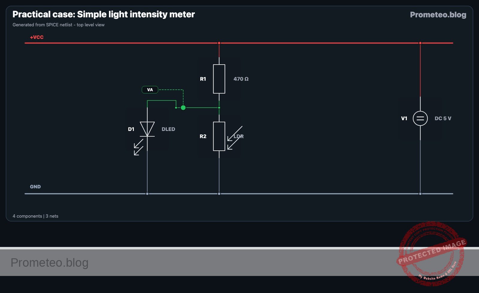
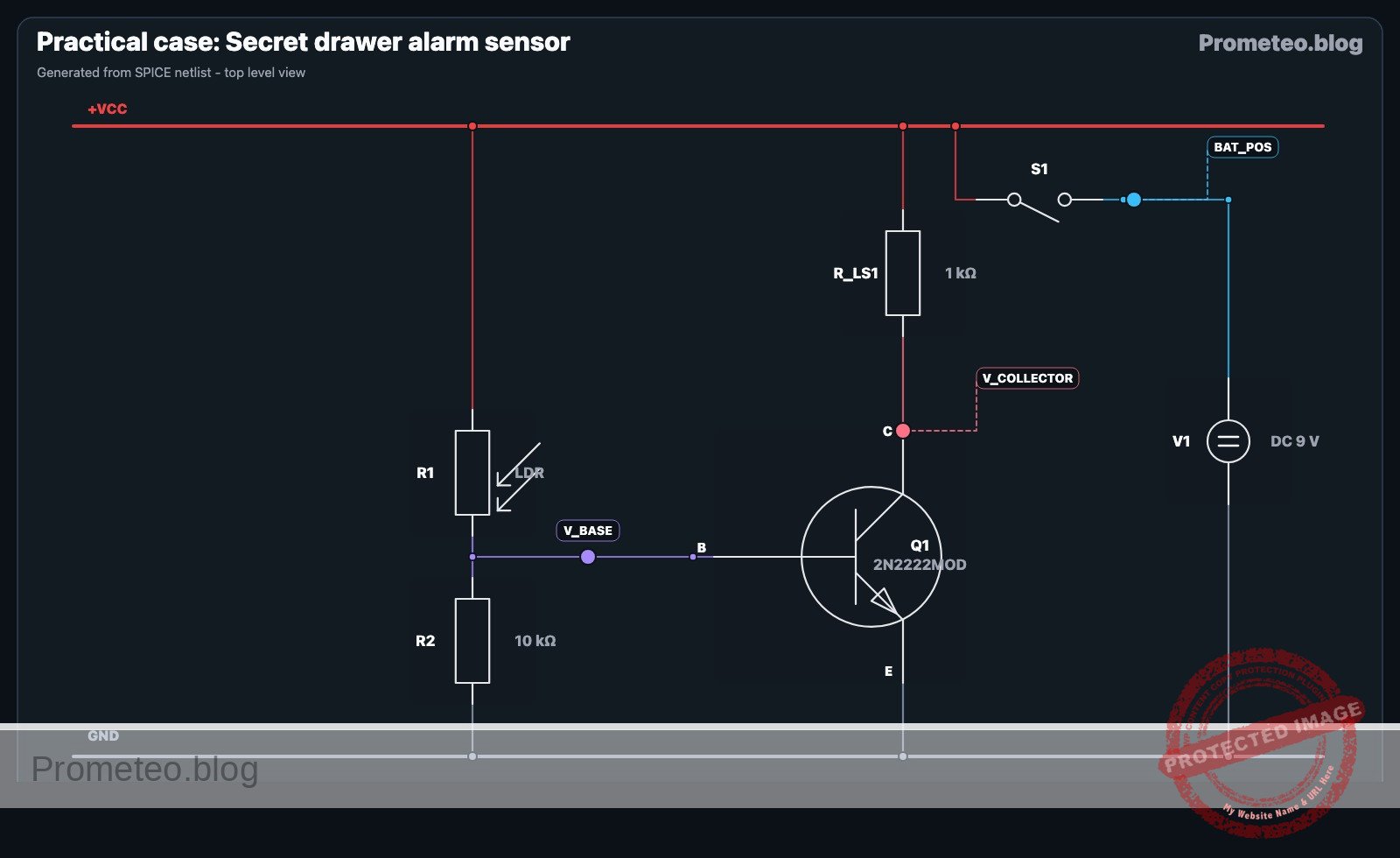
Materials
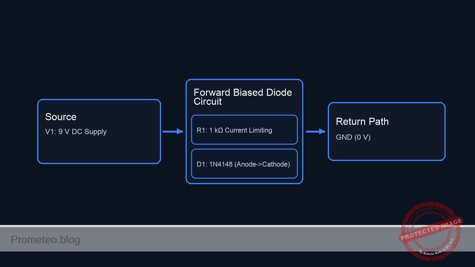
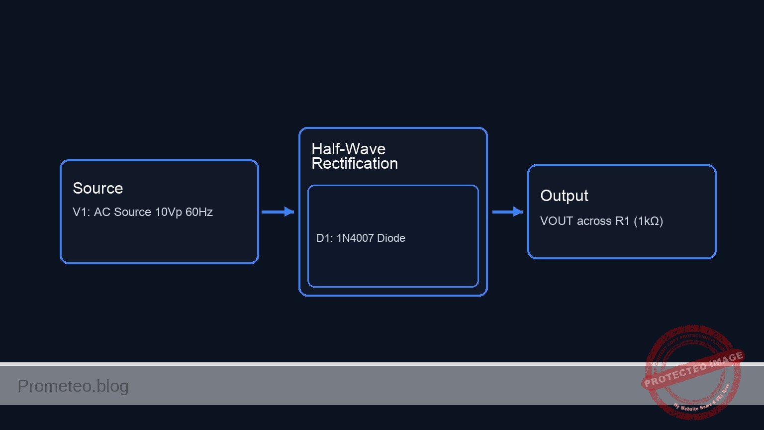
- V1: 10 V (peak), 60 Hz AC voltage source (sine wave), function: main power input.
- D1: 1N4007 (or 1N4148), function: rectifier diode.
- R1: 1 kΩ resistor, function: resistive load.
Wiring guide
This guide defines the connections between components using specific node names (VIN, VOUT, 0).
- V1 (Source): Connect the positive terminal to node
VINand the negative terminal to node0(GND). - D1 (Diode): Connect the Anode to node
VINand the Cathode (marked with a stripe) to nodeVOUT. - R1 (Load): Connect one terminal to node
VOUTand the other terminal to node0(GND).
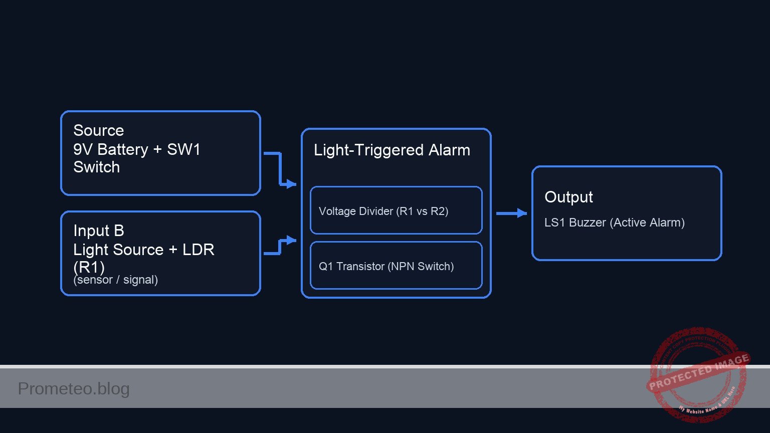
Conceptual block diagram
Schematic
[ SOURCE / INPUT ]             [ RECTIFICATION ]               [ LOAD / OUTPUT ]

[ V1: AC Source    ]           +----------------------+           [ R1: Resistor   ]
[ 10 V Peak, 60Hz   ] --(VIN)-->| Anode (A) -> Cathode | --(VOUT)--> [ 1 kΩ         ] --> GND
                               | D1: 1N4007           |
                               +----------------------+
Measurements and tests
To validate the circuit, you will need a dual-channel oscilloscope or a simulation tool.
- Setup Probes:
- Connect Channel A (Yellow) to
VINto monitor the source. - Connect Channel B (Blue) to
VOUTto monitor the voltage across the resistor. - Ensure the ground clips of both probes are connected to node
0(GND).
- Connect Channel A (Yellow) to
- Visual Inspection:
- Observe that
VINis a full sine wave centered at 0 V. - Observe that
VOUTfollowsVINduring the positive cycle but stays flat at 0 V during the negative cycle.
- Observe that
- Cursor Measurement:
- Measure the peak voltage of
VIN(e.g., 10.0 V). - Measure the peak voltage of
VOUT. It should be approximately 9.3 V. - Calculate the difference (Vin – Vout). This confirms the roughly 0.7 V forward voltage drop of the silicon diode.
- Measure the peak voltage of
SPICE netlist and simulation
Reference SPICE Netlist (ngspice) — excerptFull SPICE netlist (ngspice)
* Practical case: Simple half-wave rectification

* --- Circuit Description ---
* V1 (Source): 10V Peak, 60Hz Sine Wave
* D1 (Diode): 1N4007 Rectifier
* R1 (Load): 1k Ohm Resistor

* --- Components ---

* V1: Main power input
* Connected: Positive -> VIN, Negative -> 0 (GND)
* Syntax: SIN(Voffset Vamp Freq)
V1 VIN 0 SIN(0 10 60)

* D1: Rectifier diode (1N4007)
* Connected: Anode -> VIN, Cathode -> VOUT
D1 VIN VOUT 1N4007

* R1: Resistive load
* Connected: VOUT -> 0 (GND)
* ... (truncated in public view) ...
Copy this content into a .cir file and run with ngspice.
* Practical case: Simple half-wave rectification

* --- Circuit Description ---
* V1 (Source): 10V Peak, 60Hz Sine Wave
* D1 (Diode): 1N4007 Rectifier
* R1 (Load): 1k Ohm Resistor

* --- Components ---

* V1: Main power input
* Connected: Positive -> VIN, Negative -> 0 (GND)
* Syntax: SIN(Voffset Vamp Freq)
V1 VIN 0 SIN(0 10 60)

* D1: Rectifier diode (1N4007)
* Connected: Anode -> VIN, Cathode -> VOUT
D1 VIN VOUT 1N4007

* R1: Resistive load
* Connected: VOUT -> 0 (GND)
R1 VOUT 0 1k

* --- Models ---
* Standard model for 1N4007 Diode
.model 1N4007 D (IS=7.69n RS=0.042 N=1.45 BV=1000 IBV=5u CJO=14.2p VJ=0.5 M=0.333 TT=4.32u)

* --- Analysis Commands ---
* Transient analysis
* Frequency is 60Hz (Period ~16.67ms).
* Simulate for 50ms to capture approximately 3 full cycles.
.tran 0.1ms 50ms

* Operating Point for initial check
.op

* --- Output Directives ---
* Print input voltage and rectified output voltage
.print tran V(VIN) V(VOUT)

.end
Simulation Results (Transient Analysis)

Show raw data table (515 rows)
Index   time            v(vin)          v(vout)
0	0.000000e+00	0.000000e+00	-2.01593e-21
1	1.000000e-06	3.769911e-03	5.704546e-05
2	2.000000e-06	7.539822e-03	5.927562e-05
3	4.000000e-06	1.507964e-02	6.305993e-05
4	8.000000e-06	3.015924e-02	7.111847e-05
5	1.600000e-05	6.031821e-02	1.021853e-04
6	3.200000e-05	1.206342e-01	3.070797e-04
7	5.378437e-05	2.027484e-01	2.167324e-03
8	7.424258e-05	2.798514e-01	1.250260e-02
9	9.741093e-05	3.671480e-01	4.715921e-02
10	1.262516e-04	4.757778e-01	1.182339e-01
11	1.839330e-04	6.928557e-01	2.983890e-01
12	2.467131e-04	9.287461e-01	5.130162e-01
13	3.467131e-04	1.303359e+00	8.676123e-01
14	4.467131e-04	1.676120e+00	1.226655e+00
15	5.467131e-04	2.046499e+00	1.587509e+00
16	6.467131e-04	2.413969e+00	1.947514e+00
17	7.467131e-04	2.778010e+00	2.305173e+00
18	8.467131e-04	3.138102e+00	2.659882e+00
19	9.467131e-04	3.493735e+00	3.010809e+00
20	1.046713e-03	3.844404e+00	3.357375e+00
21	1.146713e-03	4.189609e+00	3.698904e+00
22	1.246713e-03	4.528861e+00	4.034877e+00
23	1.346713e-03	4.861677e+00	4.364712e+00
... (491 more rows) ...
Common mistakes and how to avoid them
- Reversing the diode:
- Error: The diode is installed with the cathode pointing toward the source.
- Result: The circuit produces negative voltage pulses instead of positive ones.
- Solution: Verify the stripe (cathode) points toward the load resistor.
- Ignoring power ratings:
- Error: Using a very small resistor (e.g., 10 Ω) with a standard 1/4W resistor.
- Result: The resistor overheats and burns.
- Solution: Calculate power (P = V^2 / R) or use a resistor value like 1 kΩ or higher for demonstration purposes.
- Floating Ground:
- Error: Measuring
VOUTwithout a common ground reference between the source and the oscilloscope. - Result: Noisy or floating signals on the screen.
- Solution: Ensure all grounds (Source, Resistor, Oscilloscope) are tied to node
0.
- Error: Measuring
Troubleshooting
- Symptom: No output voltage (0 V flatline).
- Cause: Diode is open (blown) or disconnected.
- Fix: Check continuity with a multimeter; replace the diode.
- Symptom: Output is identical to Input (full sine wave).
- Cause: Diode is shorted internally.
- Fix: Replace the diode; a shorted diode acts like a wire.
- Symptom: Output peak is significantly lower than expected (e.g., 5 V drop).
- Cause: High internal resistance of the source or an incorrect component (e.g., using a Zener diode in reverse breakdown).
- Fix: Verify the diode part number is a standard rectifier (1N400x series).
Possible improvements and extensions
- Filter Capacitor: Connect a capacitor (e.g., 10 µF) in parallel with R1 to observe how the capacitor fills in the gaps between pulses, smoothing the DC output.
- Full-Wave Bridge: Replace the single diode with four diodes (bridge configuration) to utilize both the positive and negative halves of the AC cycle, improving efficiency.
More Practical Cases on Prometeo.blog
Find this product and/or books on this topic on Amazon
As an Amazon Associate, I earn from qualifying purchases. If you buy through this link, you help keep this project running.
Quick Quiz

Telecommunications Electronics Engineer and Computer Engineer (official degrees in Spain).