Level: Basic. Objective: Understand how output voltage varies when modifying resistance in a potentiometer connected as a voltage divider.
Objective and use case
You will build a variable voltage divider circuit using a linear potentiometer to generate an adjustable analog voltage signal ranging from 0 V to the supply voltage.
-
Why it is useful:
- Used in volume knobs for audio equipment.
- Provides reference voltages for comparators and operational amplifiers.
- Simulates analog sensor data (like temperature or light) during testing.
- Acts as a control signal for dimmers and motor speed controllers.
- Essential for calibrating sensitivity in sensor circuits.
-
Expected outcome:
- The output voltage (VOUT) varies smoothly from 0 V to 5 V.
- At the mechanical midpoint of a linear potentiometer, VOUT reads approximately 2.5 V.
- The sum of voltage across the upper section and voltage across the lower section equals the source voltage (VIN).
-
Target audience and level: Students and electronics hobbyists (Level: Basic).
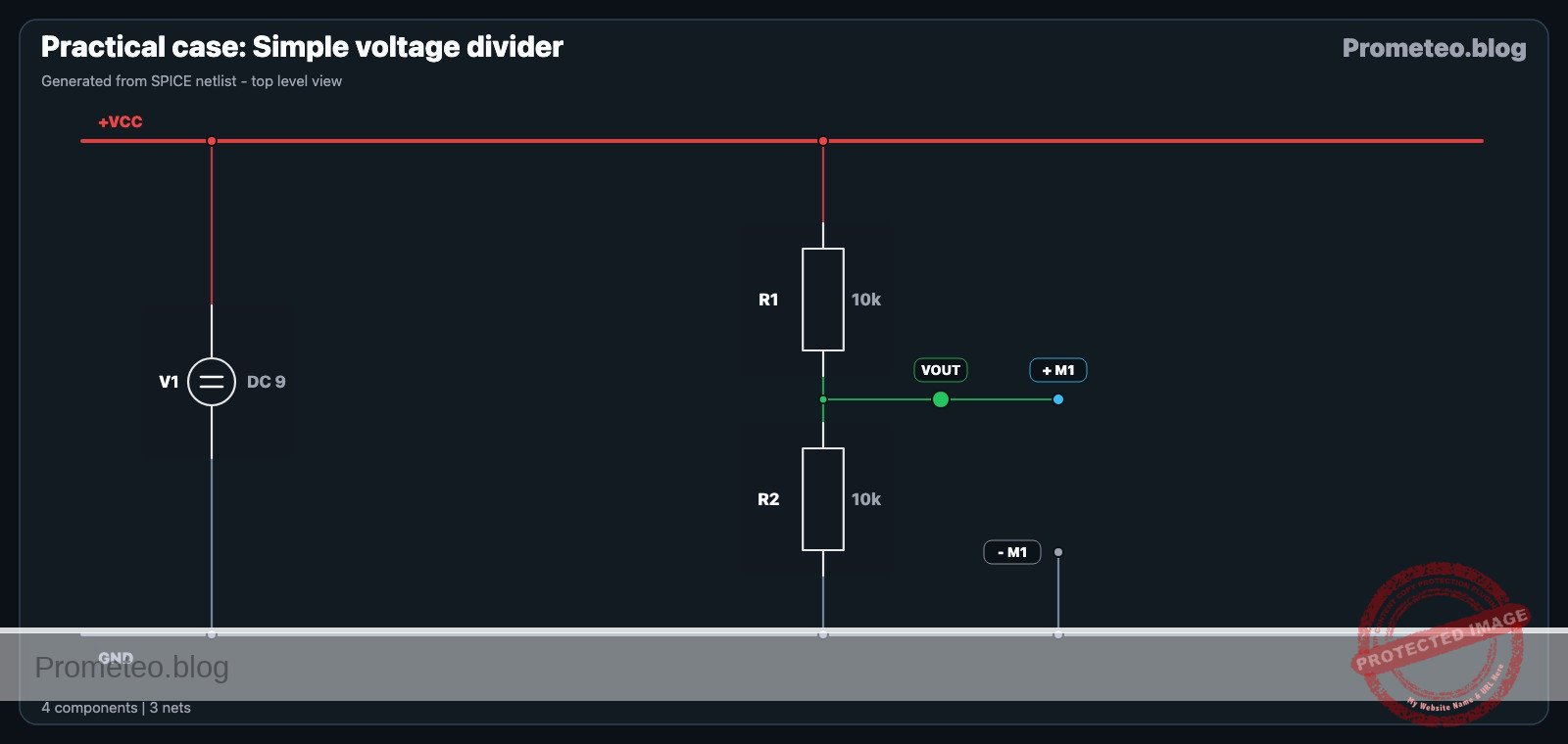
Materials
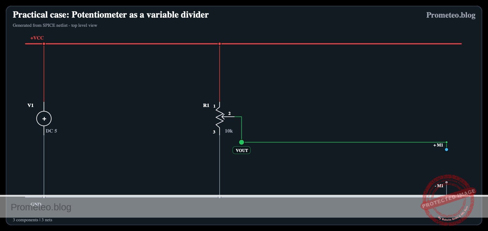
- V1: 5 V DC supply, function: main power source.
- R1: 10 kΩ linear potentiometer, function: variable voltage divider.
- M1: Digital Multimeter (set to DC Volts), function: measure V_OUT.
- W1: Jumper wires, function: interconnections.
Wiring guide
This circuit uses standard SPICE node naming conventions (VCC, 0 for GND, VOUT).
- V1 (Positive Terminal): Connects to node
VCC. - V1 (Negative Terminal): Connects to node
0(GND). - R1 (Pin 1 – Top/Fixed): Connects to node
VCC. - R1 (Pin 3 – Bottom/Fixed): Connects to node
0(GND). - R1 (Pin 2 – Wiper/Variable): Connects to node
VOUT. - M1 (Positive Probe): Connects to node
VOUT. - M1 (Negative Probe): Connects to node
0(GND).
Conceptual block diagram

Schematic
[ SOURCE ]                       [ COMPONENT ]                     [ MEASUREMENT ]

[ V1: 5 V Supply (+) ] --(Node VCC)--> [ R1: Pin 1 (Top)    ]
                                      |                    |
                                      |  Potentiometer     |
                                      |  (Voltage Divider) |
                                      |                    |
                                      |  R1: Pin 2 (Wiper) ] --(Node VOUT)--> [ M1: Multimeter (+) ]
                                      |                    |
[ V1: 5 V Supply (-) ] --(Node 0)----> [ R1: Pin 3 (Bottom) ] --(Node 0)-----> [ M1: Multimeter (-) ]
Electrical diagram
Measurements and tests
Follow these steps to validate the voltage divider behavior:
- Setup: Configure the multimeter to measure DC Voltage (20 V range). Connect the black probe to Ground (
0) and the red probe to the potentiometer wiper (VOUT). - Minimum Check: Rotate the potentiometer knob fully counter-clockwise.
- Observation: The multimeter should read roughly 0 V.
- Maximum Check: Rotate the potentiometer knob fully clockwise.
- Observation: The multimeter should read roughly 5 V (or equal to your specific V1 voltage).
- Midpoint Check: Rotate the knob to the approximate physical center.
- Observation: The multimeter should read approximately 2.5 V.
- Linearity Test: Turn the knob slowly from one end to the other.
- Observation: The voltage reading should change smoothly without jumps.
SPICE netlist and simulation
Reference SPICE Netlist (ngspice) — excerptFull SPICE netlist (ngspice)
* Practical case: Potentiometer as a variable divider

* --- Power Supply ---
* V1: 5V Main power source
* Connected to VCC (+) and 0 (GND)
V1 VCC 0 DC 5

* --- Simulation Control Source ---
* Vknob simulates the mechanical action of the potentiometer.
* Sweeps from 0 (0%) to 1 (100%) over 500us.
Vknob knob 0 PWL(0 0 500u 1)

* --- R1: 10k Potentiometer ---
* Implemented as two behavioral voltage sources (B-sources) acting as variable resistors.
* This allows the "Variable Divider" behavior to be simulated in Transient analysis.
* Total Resistance ~ 10k.

* R1 Top Part (Pin 1 to Pin 2): Connects VCC to VOUT
* Resistance = 10k * (1 - Knob) + 1 ohm (offset to avoid divide-by-zero/shorts)
B_R1_top VCC VOUT V = I(B_R1_top) * (10000 * (1 - V(knob)) + 1)
* ... (truncated in public view) ...
Copy this content into a .cir file and run with ngspice.
* Practical case: Potentiometer as a variable divider

* --- Power Supply ---
* V1: 5V Main power source
* Connected to VCC (+) and 0 (GND)
V1 VCC 0 DC 5

* --- Simulation Control Source ---
* Vknob simulates the mechanical action of the potentiometer.
* Sweeps from 0 (0%) to 1 (100%) over 500us.
Vknob knob 0 PWL(0 0 500u 1)

* --- R1: 10k Potentiometer ---
* Implemented as two behavioral voltage sources (B-sources) acting as variable resistors.
* This allows the "Variable Divider" behavior to be simulated in Transient analysis.
* Total Resistance ~ 10k.

* R1 Top Part (Pin 1 to Pin 2): Connects VCC to VOUT
* Resistance = 10k * (1 - Knob) + 1 ohm (offset to avoid divide-by-zero/shorts)
B_R1_top VCC VOUT V = I(B_R1_top) * (10000 * (1 - V(knob)) + 1)

* R1 Bottom Part (Pin 2 to Pin 3): Connects VOUT to GND
* Resistance = 10k * Knob + 1 ohm
B_R1_bot VOUT 0 V = I(B_R1_bot) * (10000 * V(knob) + 1)

* --- M1: Digital Multimeter ---
* Function: Measure V_OUT.
* Modeled as a high input impedance load (10 Megohm) connected to VOUT and GND.
R_M1 VOUT 0 10Meg

* --- Analysis Commands ---
* Transient analysis to capture the full sweep of the potentiometer (500us)
.tran 1u 500u

* Print the Output Voltage and the Control Signal (Knob position)
.print tran V(VOUT) V(knob)

* Calculate DC operating point
.op

.end
Simulation Results (Transient Analysis)

Show raw data table (508 rows)
Index   time            v(vout)         v(knob)
0	0.000000e+00	4.999000e-04	0.000000e+00
1	1.000000e-08	5.998800e-04	2.000000e-05
2	2.000000e-08	6.998599e-04	4.000000e-05
3	4.000000e-08	8.998199e-04	8.000000e-05
4	8.000000e-08	1.299740e-03	1.600000e-04
5	1.600000e-07	2.099579e-03	3.200000e-04
6	3.200000e-07	3.699258e-03	6.400000e-04
7	6.400000e-07	6.898613e-03	1.280000e-03
8	1.280000e-06	1.329731e-02	2.560000e-03
9	2.280000e-06	2.329525e-02	4.560000e-03
10	3.280000e-06	3.329314e-02	6.560000e-03
11	4.280000e-06	4.329099e-02	8.560000e-03
12	5.280000e-06	5.328880e-02	1.056000e-02
13	6.280000e-06	6.328657e-02	1.256000e-02
14	7.280000e-06	7.328430e-02	1.456000e-02
15	8.280000e-06	8.328200e-02	1.656000e-02
16	9.280000e-06	9.327965e-02	1.856000e-02
17	1.028000e-05	1.032773e-01	2.056000e-02
18	1.128000e-05	1.132749e-01	2.256000e-02
19	1.228000e-05	1.232724e-01	2.456000e-02
20	1.328000e-05	1.332699e-01	2.656000e-02
21	1.428000e-05	1.432674e-01	2.856000e-02
22	1.528000e-05	1.532648e-01	3.056000e-02
23	1.628000e-05	1.632622e-01	3.256000e-02
... (484 more rows) ...
Common mistakes and how to avoid them
- Floating the wiper: Connecting only the two fixed legs of the potentiometer makes it act as a fixed resistor. Always connect the middle pin (wiper) to your output node.
- Shorting the supply: Connecting the wiper to
VCCand one fixed leg to0, then turning the knob fully to the grounded side creates a short circuit. Ensure fixed legs go to Power and Ground, and the Wiper is the Output. - Using a Logarithmic Potentiometer: Audio taper (Log) pots change resistance non-linearly. For a predictable voltage divider test, ensure you use a Linear taper (usually marked ‘B’).
Troubleshooting
- Symptom: Voltage is constant at 2.5 V regardless of knob position.
- Cause: The wiper is disconnected, or you are measuring across the fixed terminals.
- Fix: Verify the multimeter probe is connected specifically to the center pin (wiper).
- Symptom: Smoke or heat coming from the potentiometer.
- Cause: Short circuit created by wiring the wiper to a rail and turning it to the opposite rail.
- Fix: Immediately disconnect power. Re-wire so that the fixed outer pins connect to VCC and GND, and the wiper connects only to the high-impedance meter.
- Symptom: Voltage jumps erratically (e.g., 1 V -> 4 V -> 2 V).
- Cause: Dirty or defective internal track (wiper losing contact).
- Fix: Replace the potentiometer or clean it with contact cleaner.
Possible improvements and extensions
- Loading Effect: Connect a 1 kΩ fixed resistor between
VOUTand0. Observe how the output voltage drops significantly compared to the unloaded state, demonstrating impedance mismatch. - Safe Limits: Add a 330 Ω fixed resistor in series with the top leg and another with the bottom leg. This restricts the output range (e.g., 0.5 V to 4.5 V) and protects the potentiometer from short circuits if the output is accidentally grounded.
More Practical Cases on Prometeo.blog
Find this product and/or books on this topic on Amazon
As an Amazon Associate, I earn from qualifying purchases. If you buy through this link, you help keep this project running.
Quick Quiz

Telecommunications Electronics Engineer and Computer Engineer (official degrees in Spain).