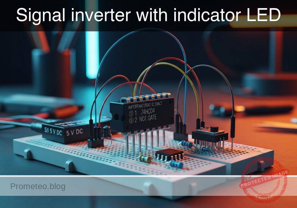
Level: Basic. Objective: Build a logic circuit using a NOT gate that activates an LED when a switch contact is opened.
Objective and use use case
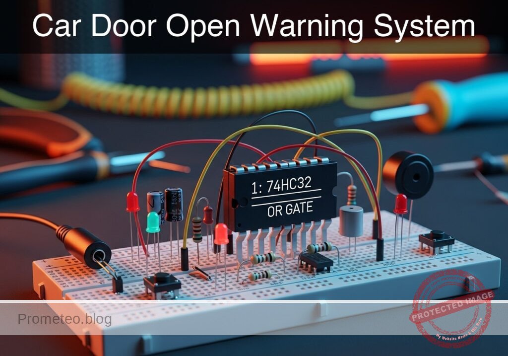
You will build a digital monitoring circuit that illuminates an LED indicator whenever a switch (representing a door sensor) breaks contact. This demonstrates the fundamental operation of the NOT gate (Inverter) in security logic.
-
Why it is useful:
- Home Security: Basic principle behind magnetic reed switches used on windows and doors.
- Appliance Safety: Ensures devices like microwaves or washing machines do not run if the door is open.
- Industrial Interlocks: Visual warning systems for machine guards.
-
Expected outcome:
- Door Closed (Switch Closed): Input logic High (5V), Output logic Low (0V), LED OFF.
- Door Open (Switch Open): Input logic Low (0V), Output logic High (5V), LED ON.
- Target audience and level: Introductory Electronics Students (Basic).
Materials
- V1: 5 V DC supply, function: Main power source
- U1: 74HC04, function: Hex Inverter (NOT gate logic)
- SW1: SPST Switch, function: Simulates door sensor (Closed = Door Closed)
- R1: 10 kΩ resistor, function: Pull-down for U1 input
- R2: 330 Ω resistor, function: LED current limiting
- D1: Red LED, function: Visual alarm indicator
Pin-out of the IC used
Chip: 74HC04 (Hex Inverter)
| Pin | Name | Logic function | Connection in this case |
|---|---|---|---|
| 1 | 1A | Input | Connected to SW1 and R1 |
| 2 | 1Y | Output | Connected to LED resistor R2 |
| 7 | GND | Ground | Connected to 0V (Power Supply Ground) |
| 14 | VCC | Power | Connected to 5V (Power Supply Positive) |
Wiring guide
- VCC connects to V1 positive terminal, U1 pin 14, and one side of SW1.
- 0 (GND) connects to V1 negative terminal, U1 pin 7, R1, and cathode of D1.
- DOOR_STATUS (Node A) connects to the other side of SW1, the other side of R1, and U1 pin 1.
- ALARM_OUT (Node Y) connects to U1 pin 2 and one side of R2.
- LED_ANODE connects to the other side of R2 and the anode of D1.
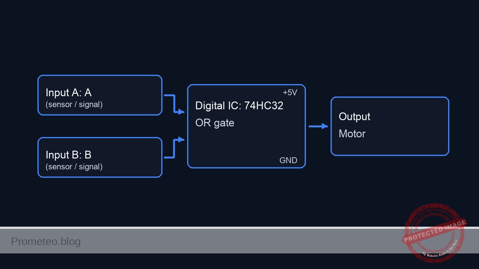
Conceptual block diagram

Schematic
[ INPUT / SENSOR ]                 [ LOGIC PROCESSING ]               [ OUTPUT / ALARM ]

    [ VCC (5V Source) ]
             |
             v
    [ SW1 (Door Switch) ]
             |
             v
          (Node A) -------------------->+------------------+
             |                          |    U1: 74HC04    |
             v                          |    (NOT Gate)    | --(Pin 2)--> [ R2: 330Ω ] --> [ D1: LED ] --> GND
    [ R1 (10k Pull-down) ]              |  Input: Pin 1    |
             |                          +------------------+
             v
            GND
Truth table
| Door Status | Switch (SW1) | Input Voltage (Pin 1) | Logic Input | Logic Output (Pin 2) | LED Status |
|---|---|---|---|---|---|
| Closed | Closed | 5 V (High) | 1 | 0 | OFF |
| Open | Open | 0 V (Low) | 0 | 1 | ON |
Measurements and tests
- Supply Check: Before inserting the IC, verify V1 provides exactly 5 V.
- State 1 (Secure): Close SW1. Measure voltage at Pin 1 (Input). It should be ~5 V. Measure Pin 2 (Output). It should be ~0 V. Verify LED is OFF.
- State 2 (Alarm): Open SW1. Measure voltage at Pin 1 (Input). It should drop to 0 V (pulled down by R1). Measure Pin 2 (Output). It should rise to ~5 V. Verify LED is ON.
SPICE netlist and simulation
Reference SPICE Netlist (ngspice) — excerptFull SPICE netlist (ngspice)
* Practical case: Open door alarm
*
* BILL OF MATERIALS:
* V1: 5V DC Supply
* U1: 74HC04 Hex Inverter (Behavioral Model)
* SW1: SPST Switch (Modeled as Voltage-Controlled Switch)
* R1: 10k Pull-down Resistor
* R2: 330 Ohm Current Limiting Resistor
* D1: Red LED
*
* WIRING CONNECTIONS:
* VCC: V1(+), U1(14), SW1(1)
* GND: V1(-), U1(7), R1(2), D1(Cathode)
* DOOR_STATUS: SW1(2), R1(1), U1(1)
* ALARM_OUT: U1(2), R2(1)
* LED_ANODE: R2(2), D1(Anode)

* --- Main Power Supply ---
V1 VCC 0 DC 5

* ... (truncated in public view) ...
Copy this content into a .cir file and run with ngspice.
* Practical case: Open door alarm
*
* BILL OF MATERIALS:
* V1: 5V DC Supply
* U1: 74HC04 Hex Inverter (Behavioral Model)
* SW1: SPST Switch (Modeled as Voltage-Controlled Switch)
* R1: 10k Pull-down Resistor
* R2: 330 Ohm Current Limiting Resistor
* D1: Red LED
*
* WIRING CONNECTIONS:
* VCC: V1(+), U1(14), SW1(1)
* GND: V1(-), U1(7), R1(2), D1(Cathode)
* DOOR_STATUS: SW1(2), R1(1), U1(1)
* ALARM_OUT: U1(2), R2(1)
* LED_ANODE: R2(2), D1(Anode)

* --- Main Power Supply ---
V1 VCC 0 DC 5

* --- User Interaction (Door Sensor) ---
* Model SW1 as a voltage-controlled switch S1 driven by a pulse source.
* Logic: Control High = Switch Closed (Door Closed). Control Low = Switch Open (Door Open).
* Pulse: Starts 0V (Open/Alarm ON), goes to 5V (Closed/Alarm OFF) at 1ms, stays for 2ms.
V_SW_CTRL SW_CTRL 0 PULSE(0 5 1m 10u 10u 2m 5m)

* S1 connects VCC to DOOR_STATUS when SW_CTRL is High.
S1 VCC DOOR_STATUS SW_CTRL 0 SW_DOOR
.model SW_DOOR SW(Vt=2.5 Ron=0.1 Roff=100Meg)

* --- Pull-down Resistor ---
R1 DOOR_STATUS 0 10k

* --- 74HC04 Hex Inverter (U1) ---
* Implements NOT gate logic: ALARM_OUT = NOT(DOOR_STATUS)
* Pin mapping: 1=In, 2=Out, 7=GND, 14=VCC
XU1 DOOR_STATUS ALARM_OUT 0 VCC 74HC04_GATE

* --- Output Stage ---
R2 ALARM_OUT LED_ANODE 330
D1 LED_ANODE 0 D_RED

* --- Models and Subcircuits ---

* LED Model
.model D_RED D(IS=1e-22 RS=6 N=1.5 CJO=50p BV=5 IBV=10u)

* 74HC04 Single Gate Behavioral Model
* Pins: In Out GND VCC
.subckt 74HC04_GATE 1 2 7 14
* Continuous sigmoid function for robust NOT logic
* Vout goes Low when Vin > 2.5V, High when Vin < 2.5V
B_INV 2 7 V = V(14,7) * (1 / (1 + exp(50 * (V(1,7) - 2.5))))
.ends

* --- Simulation Directives ---
.tran 10u 5ms
.op

* --- Output Printing ---
.print tran V(DOOR_STATUS) V(ALARM_OUT) V(LED_ANODE) V(SW_CTRL)

.end
Simulation Results (Transient Analysis)

Show raw data table (1126 rows)
Index   time            v(door_status)  v(alarm_out)    v(led_anode)
0	0.000000e+00	4.999500e-04	5.000000e+00	1.842385e+00
1	1.000000e-07	4.999500e-04	5.000000e+00	1.842385e+00
2	2.000000e-07	4.999500e-04	5.000000e+00	1.842385e+00
3	4.000000e-07	4.999500e-04	5.000000e+00	1.842385e+00
4	8.000000e-07	4.999500e-04	5.000000e+00	1.842385e+00
5	1.600000e-06	4.999500e-04	5.000000e+00	1.842385e+00
6	3.200000e-06	4.999500e-04	5.000000e+00	1.842385e+00
7	6.400000e-06	4.999500e-04	5.000000e+00	1.842385e+00
8	1.280000e-05	4.999500e-04	5.000000e+00	1.842385e+00
9	2.280000e-05	4.999500e-04	5.000000e+00	1.842385e+00
10	3.280000e-05	4.999500e-04	5.000000e+00	1.842385e+00
11	4.280000e-05	4.999500e-04	5.000000e+00	1.842385e+00
12	5.280000e-05	4.999500e-04	5.000000e+00	1.842385e+00
13	6.280000e-05	4.999500e-04	5.000000e+00	1.842385e+00
14	7.280000e-05	4.999500e-04	5.000000e+00	1.842385e+00
15	8.280000e-05	4.999500e-04	5.000000e+00	1.842385e+00
16	9.280000e-05	4.999500e-04	5.000000e+00	1.842385e+00
17	1.028000e-04	4.999500e-04	5.000000e+00	1.842385e+00
18	1.128000e-04	4.999500e-04	5.000000e+00	1.842385e+00
19	1.228000e-04	4.999500e-04	5.000000e+00	1.842385e+00
20	1.328000e-04	4.999500e-04	5.000000e+00	1.842385e+00
21	1.428000e-04	4.999500e-04	5.000000e+00	1.842385e+00
22	1.528000e-04	4.999500e-04	5.000000e+00	1.842385e+00
23	1.628000e-04	4.999500e-04	5.000000e+00	1.842385e+00
... (1102 more rows) ...
Common mistakes and how to avoid them
- Floating Input: Forgetting the pull-down resistor (R1). Without R1, when the switch opens, the input pin floats and the LED may flicker or remain in an unpredictable state. Always tie CMOS inputs to a defined logic level.
- No LED Resistor: Connecting the LED directly to the 74HC04 output without R2. This can burn out the LED or damage the IC output stage due to excessive current.
- Wrong Polarity: Inserting the LED backwards (anode to ground). The LED will never light up. Ensure the longer leg (anode) faces the resistor coming from the IC.
Troubleshooting
- LED always ON: Check if SW1 is actually closing. If using a push-button, ensure it is connected to VCC. Verify R1 is connected to Ground.
- LED always OFF: Check if the 74HC04 has power (Pin 14) and Ground (Pin 7). Check LED polarity. Ensure SW1 is actually disconnecting VCC when «Open».
- LED is dim: The value of R2 might be too high (e.g., 10kΩ instead of 330Ω) or the 5V supply is sagging.
- IC gets hot: Immediate disconnect power. Check for short circuits between Output (Pin 2) and Ground, or if the chip is inserted backwards.
Possible improvements and extensions
- Audible Alarm: Connect an NPN transistor and a buzzer to the output to generate sound alongside the light when the door opens.
- Latch Circuit: Add a feedback loop or a Flip-Flop so that once the alarm triggers, it stays ON even if the door is closed again, requiring a manual reset button.
More Practical Cases on Prometeo.blog
Find this product and/or books on this topic on Amazon
As an Amazon Associate, I earn from qualifying purchases. If you buy through this link, you help keep this project running.
Quick Quiz

Telecommunications Electronics Engineer and Computer Engineer (official degrees in Spain).