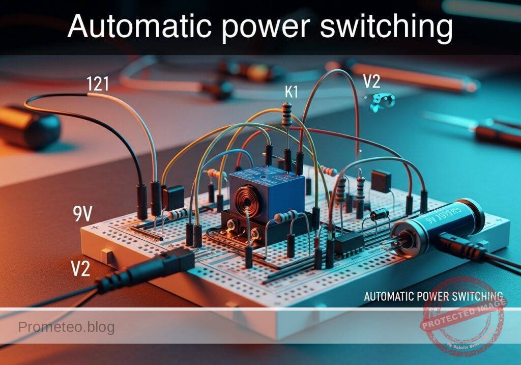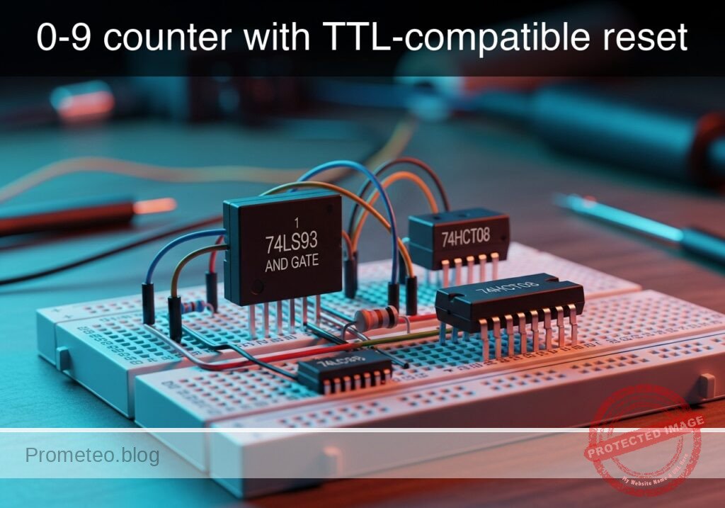
Level: Medium — Build a decimal counter that advances from 0 to 9 and resets automatically using a TTL-compatible AND gate.
Objective and use case
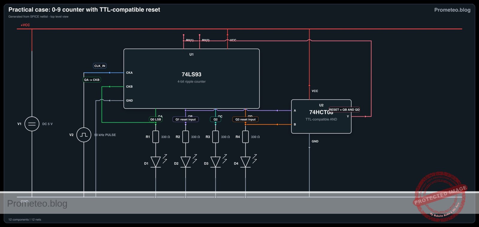
You will build a decimal counter based on a 74LS93 ripple counter and a 74HCT08 AND gate. The circuit counts from 0000 to 1001 and automatically resets when 1010 appears.
This is useful for:
– Simple event counters with a decimal display interface
– Clock divider stages for timing experiments
– Learning how asynchronous reset works in ripple counters
– Testing TTL-to-CMOS/HCT logic compatibility in mixed logic designs
Expected outcome:
– QA, QB, QC, and QD show a binary count sequence from 0 to 9
– RESET_NODE goes HIGH only when QB = 1 and QD = 1
– The counter clears immediately when state 1010 is reached
– LEDs on the four outputs visibly repeat the decimal cycle
– Logic supply remains at +5 V, with TTL-compatible levels between the 74LS93 and 74HCT08
Target audience and level: Students and technicians with basic digital electronics experience.
Materials
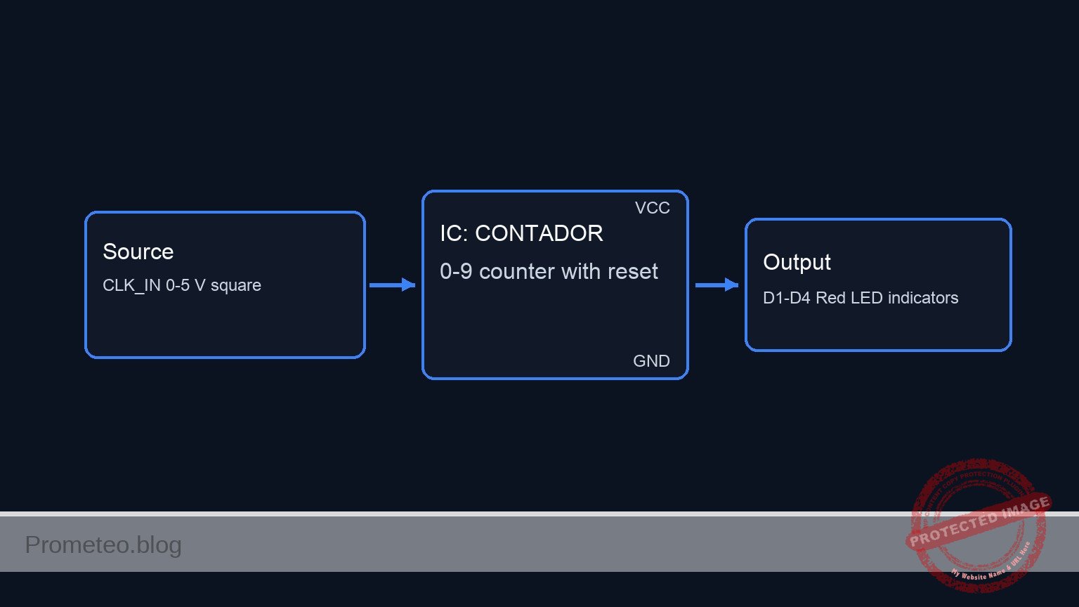
U1: 74LS93 4-bit ripple counter, function: binary count generationU2: 74HCT08 quad 2-input AND gate, function: TTL-compatible reset detectionV1: 5 V DC supply, function: power for the logic circuitX1: clock source 0-5 V square wave, function: CLK_IN signalD1: red LED, function: QA indicatorD2: red LED, function: QB indicatorD3: red LED, function: QC indicatorD4: red LED, function: QD indicatorR1: 330 Ω resistor, function: current limiting for D1R2: 330 Ω resistor, function: current limiting for D2R3: 330 Ω resistor, function: current limiting for D3R4: 330 Ω resistor, function: current limiting for D4C1: 100 nF capacitor, function: local decoupling for U1C2: 100 nF capacitor, function: local decoupling for U2
Pin-out of the IC used
74LS93
| Pin | Name | Logic function | Connection in this case |
|---|---|---|---|
| 5 | VCC | +5 V supply | VCC |
| 10 | GND | Ground | 0 |
| 14 | CP0 | Clock input A | CLK_IN |
| 1 | CP1 | Clock input B | Connected to QA for cascade |
| 2 | R0(1) | Asynchronous reset input | RESET_NODE |
| 3 | R0(2) | Asynchronous reset input | RESET_NODE |
| 12 | QA | LSB output | QA, LED D1, and feedback to CP1 |
| 9 | QB | Counter output | QB, LED D2, and reset detect input |
| 8 | QC | Counter output | QC, LED D3 |
| 11 | QD | MSB output | QD, LED D4, and reset detect input |
74HCT08
| Pin | Name | Logic function | Connection in this case |
|---|---|---|---|
| 14 | VCC | +5 V supply | VCC |
| 7 | GND | Ground | 0 |
| 1 | 1 A | AND input A | QB |
| 2 | 1B | AND input B | QD |
| 3 | 1Y | AND output | RESET_NODE |
Wiring guide
V1connects betweenVCCand0.C1connects betweenVCCand0, placed close toU1.-
C2connects betweenVCCand0, placed close toU2. -
U1pin 5 connects toVCC. U1pin 10 connects to0.U1pin 14 connects toCLK_IN.U1pin 1 connects to nodeQA.U1pin 2 connects toRESET_NODE.U1pin 3 connects toRESET_NODE.U1pin 12 connects to nodeQA.U1pin 9 connects to nodeQB.U1pin 8 connects to nodeQC.-
U1pin 11 connects to nodeQD. -
U2pin 14 connects toVCC. U2pin 7 connects to0.U2pin 1 connects to nodeQB.U2pin 2 connects to nodeQD.-
U2pin 3 connects to nodeRESET_NODE. -
R1connects betweenQAand nodeLED1_A. D1connects betweenLED1_Aand0.R2connects betweenQBand nodeLED2_A.D2connects betweenLED2_Aand0.R3connects betweenQCand nodeLED3_A.D3connects betweenLED3_Aand0.R4connects betweenQDand nodeLED4_A.D4connects betweenLED4_Aand0.
Use the 74HCT08, not the 74HC08, because the reset gate is driven by 74LS93 TTL outputs and must accept TTL-compatible HIGH levels reliably.
Conceptual block diagram
Schematic
Practical case: 0-9 counter with TTL-compatible reset (74LS93 + 74HCT08)

[ X1: CLK_IN 0-5 V square ] --> [ U1: 74LS93 4-bit Ripple Counter (CP0 pin14) ]
(Internal to U1: QA (pin12) --> CP1 (pin1) for divide-by-10 configuration)

U1 Q outputs to indicators (loads on the right):
[ U1: QA (pin12) ] --> [ R1: 330 Ω ] --> [ D1: Red LED ] --> GND
[ U1: QB (pin9)  ] --> [ R2: 330 Ω ] --> [ D2: Red LED ] --> GND
[ U1: QC (pin8)  ] --> [ R3: 330 Ω ] --> [ D3: Red LED ] --> GND
[ U1: QD (pin11) ] --> [ R4: 330 Ω ] --> [ D4: Red LED ] --> GND

Reset detection (separate branches; TTL-compatible gate):
[ Tap: U1.QB (pin9) ] -->
[ Tap: U1.QD (pin11) ] --> [ U2: 74HCT08 AND (pins 1,2→3) ] --(RESET_NODE)--> (to U1 Async Reset R0(1),R0(2) pins 2 & 3)

Power and decoupling (for completeness):
[ V1: +5 V ] --> [ U1: VCC pin5 ]          ; return GND --> (U1 GND pin10)
[ V1: +5 V ] --> [ U2: VCC pin14 ]         ; return GND --> (U2 GND pin7)
[ C1: 100 nF ] between U1 VCC and GND (place close to U1)
[ C2: 100 nF ] between U2 VCC and GND (place close to U2)
Electrical diagram
Truth table
This table corresponds to the AND gate used for reset detection.
| QB | QD | RESET_NODE |
|---|---|---|
| 0 | 0 | 0 |
| 0 | 1 | 0 |
| 1 | 0 | 0 |
| 1 | 1 | 1 |
Measurements and tests
- Power-off continuity check
- Verify
VCCis not shorted to0. - Confirm
U1reset pins 2 and 3 are tied together atRESET_NODE. -
Confirm
U1pin 1 is connected toQA. -
Power-on static check
- Apply +5 V.
- Check that
U1andU2both receive correct supply voltage. -
With no clock applied, outputs may start in an unknown state; a brief manual reset to
RESET_NODE = HIGHshould forceQA QB QC QD = 0000. -
Clock verification
- Measure
CLK_INwith an oscilloscope. - Use a slow frequency such as 1 Hz to 10 Hz for visual LED observation.
-
Confirm the clock swings approximately from 0 V to 5 V.
-
Counter sequence check
- Measure
QA,QB,QC, andQD. - Verify the sequence:
0000000100100011010001010110011110001001
-
The next attempted state is
1010, but it must reset immediately to0000. -
Reset-node validation
- Measure
RESET_NODE. - It should remain LOW for counts
0000through1001. -
It should pulse HIGH when
QB = 1andQD = 1, which corresponds to detection of1010. -
LED observation
D1must toggle at the highest visible rate.D2toggles at half theQArate.D3andD4toggle progressively slower.- The visible pattern must repeat every 10 clock pulses.
SPICE netlist and simulation
Reference SPICE Netlist (ngspice) — excerptFull SPICE netlist (ngspice)
* Practical case: Decade counter 0-9 with reset (Corrected)
.width out=256
* Fixed Impedance and Timing issues for 74LS93 ripple counter
* Ngspice compliant netlist

* --- COMPONENT MODELS ---
* Generic Red LED Model
.model DLED D(IS=1e-14 N=1.7 RS=10 BV=5 IBV=10u CJO=10p)

* --- LOGIC GATE SUBCIRCUITS (Behavioral with Low Impedance Output) ---
* IMPORTANT: Output Impedance reduced to 50 ohms to drive LEDs and avoid loading effects.
* Delays (C1=10p) maintained for convergence and latch feedback.

* Inverter (Standard Delay ~500ps)
.subckt INV A Y VCC GND
B1 Y_int 0 V = V(VCC) * (1 / (1 + exp(20 * (V(A) - 2.5))))
R1 Y_int Y 50
C1 Y 0 10p
.ends

* ... (truncated in public view) ...
Copy this content into a .cir file and run with ngspice.
* Practical case: Decade counter 0-9 with reset (Corrected)
.width out=256
* Fixed Impedance and Timing issues for 74LS93 ripple counter
* Ngspice compliant netlist

* --- COMPONENT MODELS ---
* Generic Red LED Model
.model DLED D(IS=1e-14 N=1.7 RS=10 BV=5 IBV=10u CJO=10p)

* --- LOGIC GATE SUBCIRCUITS (Behavioral with Low Impedance Output) ---
* IMPORTANT: Output Impedance reduced to 50 ohms to drive LEDs and avoid loading effects.
* Delays (C1=10p) maintained for convergence and latch feedback.

* Inverter (Standard Delay ~500ps)
.subckt INV A Y VCC GND
B1 Y_int 0 V = V(VCC) * (1 / (1 + exp(20 * (V(A) - 2.5))))
R1 Y_int Y 50
C1 Y 0 10p
.ends

* Fast Inverter (Minimal Delay ~5ps) - Used for Clock Edge logic to prevent races
.subckt INV_FAST A Y VCC GND
B1 Y_int 0 V = V(VCC) * (1 / (1 + exp(20 * (V(A) - 2.5))))
R1 Y_int Y 50
C1 Y 0 0.1p
.ends

* 2-Input NAND
.subckt NAND2 A B Y VCC GND
B1 Y_int 0 V = V(VCC) * (1 - ( (1/(1+exp(-20*(V(A)-2.5)))) * (1/(1+exp(-20*(V(B)-2.5)))) ))
R1 Y_int Y 50
C1 Y 0 10p
.ends

* 3-Input NAND
.subckt NAND3 A B C Y VCC GND
B1 Y_int 0 V = V(VCC) * (1 - ( (1/(1+exp(-20*(V(A)-2.5)))) * (1/(1+exp(-20*(V(B)-2.5)))) * (1/(1+exp(-20*(V(C)-2.5)))) ))
R1 Y_int Y 50
C1 Y 0 10p
.ends

* 2-Input AND
.subckt AND2 A B Y VCC GND
B1 Y_int 0 V = V(VCC) * ( (1/(1+exp(-20*(V(A)-2.5)))) * (1/(1+exp(-20*(V(B)-2.5)))) )
R1 Y_int Y 50
C1 Y 0 10p
.ends

* --- FLIP-FLOP SUBCIRCUIT ---
* T-FlipFlop: Negative Edge Triggered with Active High Clear
* Uses INV_FAST for clock inversion to ensure Master-Slave non-overlap (Race Fix).
.subckt TFF_NEG_CLR CLK CLR Q QBAR VCC GND
* Invert Clear
XINV_CLR CLR CLR_BAR VCC GND INV

* Invert Clock FAST (Avoids race where both Master and Slave are transparent)
XINV_CLK CLK CLK_BAR VCC GND INV_FAST

* -- Master Latch (Tracks D=QBAR when CLK=1) --
XG1 QBAR CLK M_SET_BAR VCC GND NAND2
XG2 Q CLK CLR_BAR M_RST_BAR VCC GND NAND3
XL1 M_SET_BAR M_QBAR M_Q VCC GND NAND2
XL2 M_RST_BAR M_Q CLR_BAR M_QBAR VCC GND NAND3

* -- Slave Latch (Tracks Master when CLK=0 -> CLK_BAR=1) --
* Uses CLK_BAR which is delayed only slightly less than gates, ensuring clean handover.
XG3 M_Q CLK_BAR S_SET_BAR VCC GND NAND2
XG4 M_QBAR CLK_BAR S_RST_BAR VCC GND NAND2
XL3 S_SET_BAR QBAR Q VCC GND NAND2
XL4 S_RST_BAR Q CLR_BAR QBAR VCC GND NAND3
.ends

* --- IC SUBCIRCUITS ---

* U1: 74LS93 4-Bit Binary Counter
* Pinout mapping adjusted to match standard 14-pin DIP in netlist order:
* 1=IN_B, 2=R0(1), 3=R0(2), 5=VCC, 8=QC, 9=QB, 10=GND, 11=QD, 12=QA, 14=IN_A
.subckt 74LS93 IN_B R0_1 R0_2 VCC QC QB GND QD QA IN_A
* Internal Reset Logic: Reset if R0_1 AND R0_2 are High
XAND_RST R0_1 R0_2 RESET VCC GND AND2

* Section 1: 1-bit counter (Input A -> QA)
XFFA IN_A RESET QA QA_BAR VCC GND TFF_NEG_CLR

* Section 2: 3-bit ripple counter (Input B -> QB -> QC -> QD)
XFFB IN_B RESET QB QB_BAR VCC GND TFF_NEG_CLR
XFFC QB RESET QC QC_BAR VCC GND TFF_NEG_CLR
XFFD QC RESET QD QD_BAR VCC GND TFF_NEG_CLR
.ends

* U2: 74HCT08 Quad 2-Input AND Gate
* HCT input thresholds are TTL-compatible, so 74LS93 HIGH outputs
* reliably drive the reset-detect gate in a real classroom build.
* Pins: 1=1A, 2=1B, 3=1Y, 7=GND, 14=VCC
.subckt 74HCT08 1A 1B 1Y GND VCC
XG1 1A 1B 1Y VCC GND AND2
.ends

* --- MAIN CIRCUIT ---

* 1. Power Supply
V1 VCC 0 DC 5

* 2. Clock Signal (50kHz)
V2 CLK_IN 0 PULSE(0 5 1u 100n 100n 10u 20u)

* 3. U1: 74LS93 Counter
* Wiring Guide connections:
* Pin 1 (CKB) connects to QA_NODE (Cascade)
* Pin 12 (QA) connects to QA_NODE
* Pin 14 (CKA) connects to CLK_IN
* Pin 2, 3 connect to RESET_NODE
* Outputs to LEDs
XU1 QA_NODE RESET_NODE RESET_NODE VCC QC_NODE QB_NODE 0 QD_NODE QA_NODE CLK_IN 74LS93

* 4. U2: 74HCT08 Reset Logic
* Reset when Count=10 (Binary 1010 -> QD=1, QB=1)
* Inputs: QB_NODE, QD_NODE -> Output: RESET_NODE
XU2 QB_NODE QD_NODE RESET_NODE 0 VCC 74HCT08

* 5. LED Indicators (with Current Limiting Resistors)
* Bit 0 (QA)
R1 QA_NODE N_D1 330
D1 N_D1 0 DLED

* Bit 1 (QB)
R2 QB_NODE N_D2 330
D2 N_D2 0 DLED

* Bit 2 (QC)
R3 QC_NODE N_D3 330
D3 N_D3 0 DLED

* Bit 3 (QD)
R4 QD_NODE N_D4 330
D4 N_D4 0 DLED

* --- SIMULATION COMMANDS ---
.op
* Transient analysis: 500us to see counts 0-9 and reset
.tran 100n 500u

* Print essential nodes. CLK_IN first.
.print tran V(CLK_IN) V(QA_NODE) V(QB_NODE) V(QC_NODE) V(QD_NODE) V(RESET_NODE)

.end
* --- GPT review (BOM/Wiring/SPICE) ---
* circuit_ok=true
* simulation_summary: The simulation successfully demonstrates a 4-bit counting sequence. The counter increments on the falling edge of the clock. The reset logic triggers correctly when the count reaches 10 (Binary 1010: QD=High, QB=High), forcing the outputs back to 0 immediately, effectively creating a 0-9 decade counter.
* bom_vs_spice equivalences ignored:
*   - Clock source V2 modeled as a PULSE voltage source.
*   - LEDs (D1-D4) modeled as generic diodes with specific parameters (DLED).
*   - U1 (74LS93) modeled as a behavioral subcircuit using flip-flops and logic gates.
*   - U2 (74HCT08) modeled as a behavioral subcircuit using AND gates.
* overall_comment: The circuit is well-designed and the SPICE netlist accurately reflects the intended decade counter logic. The behavioral models for the 74LS93 and 74HCT08 are robust, including necessary delays to prevent race conditions. The simulation logs confirm the modulo-10 reset operation works as expected. This is a solid didactic example.
* --------------------------------------
Simulation Results (Transient Analysis)

Show raw data table (6785 rows)
Index   time            v(clk_in)       v(qa_node)      v(qb_node)      v(qc_node)      v(qd_node)      v(reset_node)
0	0.000000e+00	0.000000e+00	-7.27413e-30	4.514570e+00	-7.27413e-30	-7.27411e-30	9.643749e-22
1	1.000000e-09	0.000000e+00	-6.24961e-30	4.514570e+00	-6.24960e-30	-6.24960e-30	9.643749e-22
2	2.000000e-09	0.000000e+00	-4.31599e-30	4.514570e+00	-4.31599e-30	-4.31599e-30	9.643749e-22
3	4.000000e-09	0.000000e+00	-8.63940e-32	4.514570e+00	-8.63867e-32	-8.63940e-32	9.643749e-22
4	8.000000e-09	0.000000e+00	6.051302e-30	4.514570e+00	6.051309e-30	6.051302e-30	9.643749e-22
5	1.600000e-08	0.000000e+00	8.619372e-30	4.514570e+00	8.619381e-30	8.619372e-30	9.643749e-22
6	3.200000e-08	0.000000e+00	4.420001e-30	4.514570e+00	4.420001e-30	4.419984e-30	9.643749e-22
7	6.400000e-08	0.000000e+00	-8.88725e-31	4.514570e+00	-8.88725e-31	-8.88708e-31	9.643749e-22
8	1.280000e-07	0.000000e+00	-1.16882e-30	4.514570e+00	-1.16881e-30	-1.16884e-30	9.643749e-22
9	2.280000e-07	0.000000e+00	-1.70113e-31	4.514570e+00	-1.70131e-31	-1.70113e-31	9.643749e-22
10	3.280000e-07	0.000000e+00	1.102262e-31	4.514570e+00	1.101893e-31	1.102078e-31	9.643749e-22
11	4.280000e-07	0.000000e+00	-2.09740e-32	4.514570e+00	-2.09440e-32	-2.09556e-32	9.643749e-22
12	5.280000e-07	0.000000e+00	3.730926e-32	4.514570e+00	3.729081e-32	3.729081e-32	9.643749e-22
13	6.280000e-07	0.000000e+00	-4.04764e-32	4.514570e+00	-4.04464e-32	-4.04395e-32	9.643749e-22
14	7.280000e-07	0.000000e+00	3.793658e-32	4.514570e+00	3.789968e-32	3.791813e-32	9.643749e-22
15	8.280000e-07	0.000000e+00	-3.71737e-32	4.514570e+00	-3.71437e-32	-3.71552e-32	9.643749e-22
16	9.280000e-07	0.000000e+00	3.658968e-32	4.514570e+00	3.657123e-32	3.658968e-32	9.643749e-22
17	1.000000e-06	0.000000e+00	-3.53679e-32	4.514570e+00	-3.53610e-32	-3.53496e-32	9.643749e-22
18	1.010000e-06	5.000000e-01	-2.79091e-33	4.514570e+00	-2.80820e-33	-2.79091e-33	9.643749e-22
19	1.030000e-06	1.500000e+00	1.602683e-33	4.514570e+00	1.585385e-33	1.602683e-33	9.643749e-22
20	1.048757e-06	2.437856e+00	4.312441e+00	4.514570e+00	-1.25584e-33	-1.27306e-33	9.643749e-22
21	1.062135e-06	3.106726e+00	4.691659e+00	4.514570e+00	1.096887e-33	1.103161e-33	9.643749e-22
22	1.071814e-06	3.590675e+00	4.366639e+00	4.514570e+00	-8.23695e-34	-8.33794e-34	9.643749e-22
23	1.080871e-06	4.043525e+00	4.636207e+00	4.514570e+00	6.872047e-34	7.032322e-34	9.643749e-22
... (6761 more rows) ...
Common mistakes and how to avoid them
- Using 74HC08 instead of 74HCT08
- Problem: the 74LS93 HIGH level may not meet standard HC input thresholds reliably.
-
Solution: use 74HCT08 for TTL-compatible input levels.
-
Forgetting the
QAtoCP1connection - Problem: the 74LS93 will not count correctly through the intended 4-bit sequence.
-
Solution: connect
U1pin 12 (QA) directly toU1pin 1 (CP1). -
Reset inputs not tied together
- Problem: the counter may not clear when
1010occurs. - Solution: connect both
R0(1)andR0(2)to the sameRESET_NODE.
Troubleshooting
- Symptom: The count goes beyond 9.
- Cause:
QBorQDis not correctly connected to the AND gate. -
Fix: verify
U2pin 1 =QB,U2pin 2 =QD, andU2pin 3 =RESET_NODE. -
Symptom: The circuit never counts.
- Cause:
RESET_NODEis stuck HIGH. -
Fix: check for miswiring, shorts, or swapped AND gate pins.
-
Symptom: LEDs behave randomly at power-up.
- Cause: ripple counters can power up in an undefined state.
-
Fix: apply a short reset pulse at startup.
-
Symptom: Reset is unreliable.
- Cause: wrong logic family used for the reset gate.
-
Fix: replace any 74HC08 with 74HCT08.
-
Symptom: Only the first stage toggles.
- Cause: missing cascade connection from
QAtoCP1. - Fix: reconnect
U1pin 12 toU1pin 1.
Possible improvements and extensions
- Add a BCD-to-7-segment decoder and display so the count is shown directly as digits 0 to 9.
- Replace the clock source with a debounced push-button for manual stepping and observation of each state.
More Practical Cases on Prometeo.blog
Find this product and/or books on this topic on Amazon
As an Amazon Associate, I earn from qualifying purchases. If you buy through this link, you help keep this project running.
Quick Quiz

Telecommunications Electronics Engineer and Computer Engineer (official degrees in Spain).