Level: Medium — Build a stable shadow detector with visual indication and low false triggering.
Objective and use case
You will build a photoresistor-based circuit that detects a sudden drop in light caused by a shadow and turns on an LED in a stable way. The design uses an LDR voltage divider, an RC filter, and a comparator with hysteresis to reduce false activations.
Why it is useful:
- Detect when a hand or object passes in front of a lighted opening.
- Create a simple visual warning for access points, boxes, or cabinets.
- Monitor brief shadow events in classroom experiments on light sensing.
- Add a reliable light-change trigger to small automation prototypes.
Expected outcome:
- Sensor voltage at
VAchanges with light level, typically from about 0.8 V to 4.2 V depending on illumination. - Filtered voltage at
VBchanges more slowly thanVA, reducing short spikes and flicker. - Comparator output at
VOUTswitches cleanly between low and high states. - LED
D1turns on when light drops below the adjusted threshold and remains stable near the switching point. - Hysteresis of about 0.2 V to 0.5 V avoids repeated on/off oscillation.
Target audience and level: Students with basic knowledge of resistors, capacitors, and voltage measurement.
Materials
V1: 5 V DC supplyR1: LDR photoresistor, function: light-dependent upper arm of sensor dividerR2: 10 kΩ potentiometer, function: adjustable lower arm of sensor divider and threshold tuning aidR3: 22 kΩ resistor, function: series resistor from sensor node to RC filterC1: 10 µF capacitor, function: low-pass filter for shadow event stabilizationU1: LM393 comparator, function: compare filtered sensor voltage against adjustable referenceR4: 10 kΩ potentiometer, function: reference voltage adjustment for comparatorR5: 220 kΩ resistor, function: positive feedback to add hysteresisR6: 10 kΩ resistor, function: pull-up for LM393 open-collector outputD1: red LED, function: visual alert outputR7: 330 Ω resistor, function: LED current limiting
Wiring guide
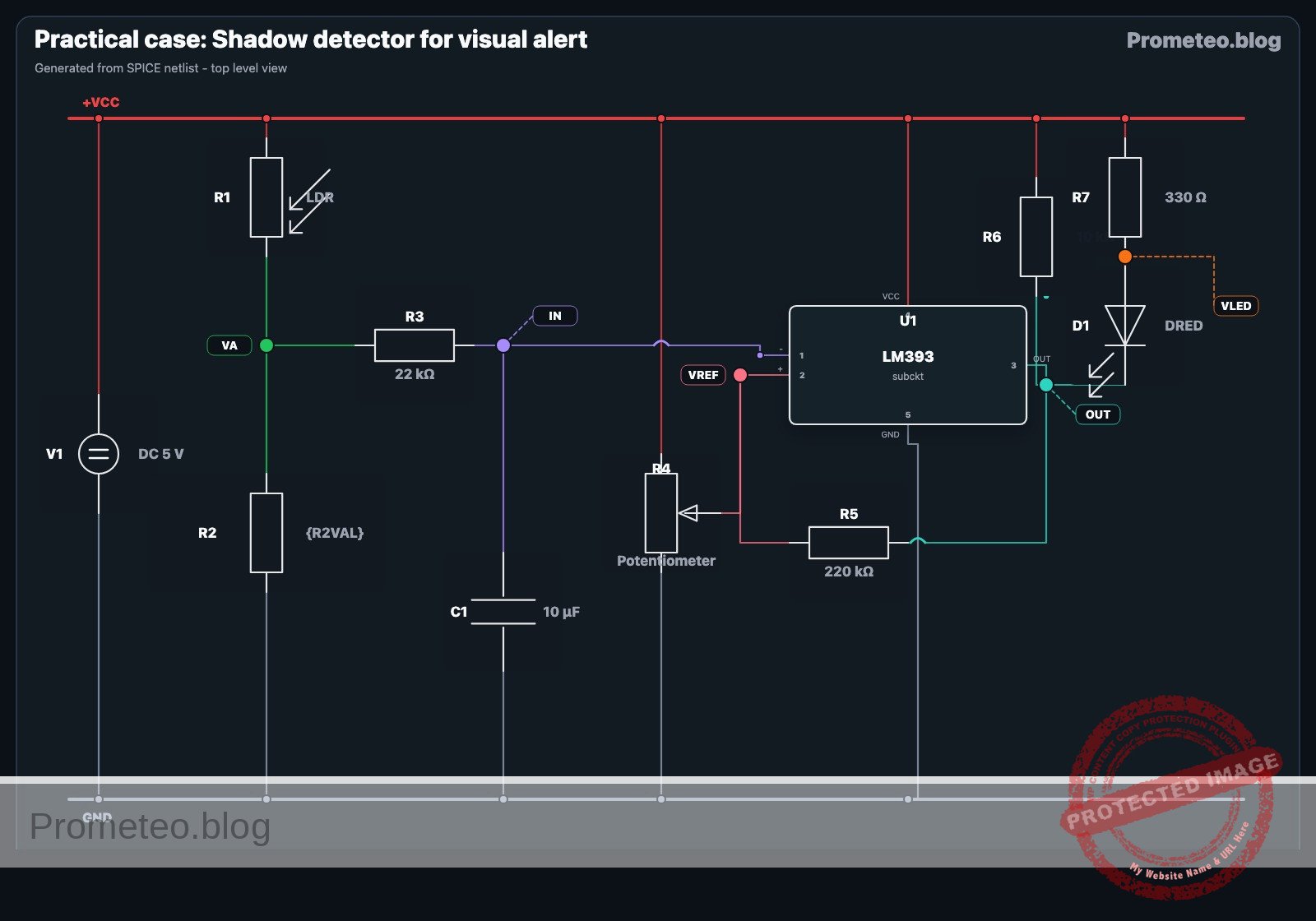
V1connects between nodesVCCand0.R1connects between nodesVCCandVA.R2connects between nodesVAand0; use the potentiometer as a variable resistor to adjust the divider sensitivity.R3connects between nodesVAandVB.C1connects between nodesVBand0.R4connects between nodesVCCand0; connect the wiper ofR4to nodeVREF.U1LM393 power pins connect as follows: supply pin toVCC, ground pin to0.U1comparator non-inverting input connects to nodeVREF.U1comparator inverting input connects to nodeVB.R5connects between nodesVOUTandVREF.R6connects between nodesVCCandVOUT.R7connects between nodesVCCandVLED.D1connects between nodesVLEDandVOUT; orient the LED so it turns on whenVOUTis pulled low byU1.
Conceptual block diagram
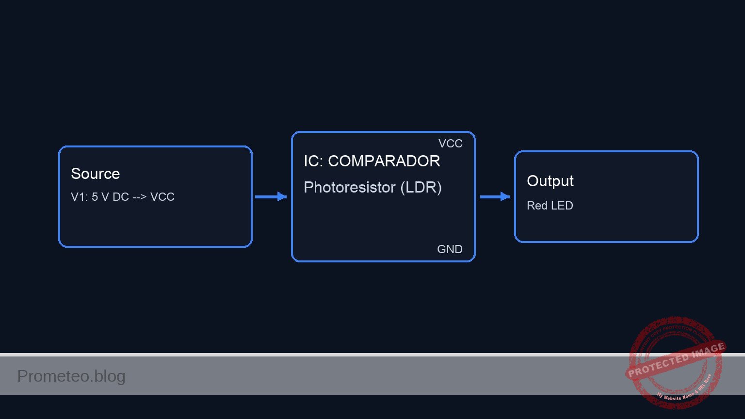
Schematic
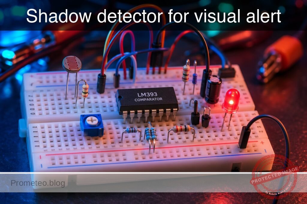
Practical case: Shadow detector for visual alert

Light / Shadow
      --> [ R1: LDR ]
      --> (VA: sensor divider node)
      --> [ R3: 22 kΩ ]
      --> (VB: filtered sensor signal)
      --> [ U1: LM393 Comparator (-) ]

VCC --> [ R2: 10 kΩ Pot, sensitivity adjust ] --> GND
                  \
                   --> (VA)

VCC --> [ R4: 10 kΩ Pot, reference adjust ] --> GND
                  \
                   --> (VREF)
                   --> [ U1: LM393 Comparator (+) ]

[ U1: LM393 Comparator Output VOUT ]
      --> [ R5: 220 kΩ Positive Feedback ] --> (VREF)
      --> [ D1: Red LED ] --> [ R7: 330 Ω ] --> VCC
      --> [ Alert Output: LED ON when VOUT goes LOW ]

VCC --> [ R6: 10 kΩ Pull-up ] --> (VOUT)

(VB) --> [ C1: 10 µF Low-Pass Filter ] --> GND

V1: 5 V DC --> VCC
V1: 0 V    --> GND
U1 power: VCC, GND
Electrical diagram
Measurements and tests
- Power-off inspection
- Check that
VCCand0are not shorted. - Confirm LED polarity.
-
Verify that the LM393 output has a pull-up resistor
R6. -
Supply check
- Power the circuit with
V1 = 5 V. -
Measure between
VCCand0; expected value:4.9 Vto5.1 V. -
Sensor voltage measurement
- Measure
VAin bright light and then under a shadow. - Expected result:
VAshould change clearly, often by more than1 V. -
If the change is too small, adjust
R2or change the light angle on the LDR. -
Filtered response measurement
- Measure
VBwhile suddenly covering the LDR. VBshould not jump instantly; it should move with a short delay set byR3 × C1.-
With
R3 = 22 kΩandC1 = 10 µF, the time constant is about0.22 s. -
Threshold adjustment
- Adjust
R4untilD1is off in normal light and turns on when a clear shadow is applied. -
Measure
VREF; typical useful range is1 Vto4 V. -
Hysteresis verification
- Slowly move a hand to create a partial shadow and then slowly remove it.
- Measure the switching voltage at
VBwhen the LED turns on and when it turns off. -
The two values should differ slightly because of
R5; a difference of0.2 Vto0.5 Vis a good target. -
Response time test
- Repeatedly create a sudden shadow and observe LED behavior.
- The LED should react within a fraction of a second, without flickering from very brief light variations.
- If the response is too slow, reduce
C1to4.7 µF. -
If false triggering remains, increase
C1to22 µFor increaseR5slightly for more hysteresis. -
False activation test
- Illuminate the LDR with room light and introduce small disturbances such as hand motion nearby but not fully covering it.
- The LED should remain stable unless the light drop is large enough to cross the threshold.
SPICE netlist and simulation
Reference SPICE Netlist (ngspice) — excerptFull SPICE netlist (ngspice)
* Practical case: Shadow detector for visual alert
.width out=256

.param R2VAL=5k
.param R4POS=0.5
.param R4TOP={10000*(1-R4POS)+1m}
.param R4BOT={10000*(R4POS)+1m}
.param RLIGHT=2k
.param RDARK=50k

V1 VCC 0 DC 5

* Dynamic light/shadow stimulus: 0 = light, 1 = shadow
VLUX LUX 0 PULSE(0 1 50m 1m 1m 200m 400m)

* R1 LDR photoresistor: upper arm of divider
R1 VCC VA r='{RLIGHT + (RDARK-RLIGHT)*V(LUX)}'

* R2 10k potentiometer used as variable resistor
R2 VA 0 {R2VAL}
* ... (truncated in public view) ...
Copy this content into a .cir file and run with ngspice.
* Practical case: Shadow detector for visual alert
.width out=256

.param R2VAL=5k
.param R4POS=0.5
.param R4TOP={10000*(1-R4POS)+1m}
.param R4BOT={10000*(R4POS)+1m}
.param RLIGHT=2k
.param RDARK=50k

V1 VCC 0 DC 5

* Dynamic light/shadow stimulus: 0 = light, 1 = shadow
VLUX LUX 0 PULSE(0 1 50m 1m 1m 200m 400m)

* R1 LDR photoresistor: upper arm of divider
R1 VCC VA r='{RLIGHT + (RDARK-RLIGHT)*V(LUX)}'

* R2 10k potentiometer used as variable resistor
R2 VA 0 {R2VAL}

R3 VA VB 22k
C1 VB 0 10u

* R4 10k potentiometer with wiper at VREF
R4A VCC VREF {R4TOP}
R4B VREF 0 {R4BOT}

* U1 LM393 approximation
* Non-inverting input: VREF
* Inverting input: VB
* Open-collector output: VOUT
B_U1DRV NBASE 0 V='0.95*(1+tanh(80*(V(VREF)-V(VB))))/2'
R_U1B NBASE 0 100k
Q_U1 VOUT NBASE 0 QLM393OC

R5 VOUT VREF 220k
R6 VCC VOUT 10k

R7 VCC VLED 330
D1 VLED VOUT DRED

* Probe aliases so .print can include V(IN) and V(OUT) first
V_INMON IN VB DC 0
V_OUTMON OUT VOUT DC 0

.model QLM393OC NPN(IS=1e-14 BF=100 VAF=100 CJE=5p CJC=3p TF=1n TR=10n)
.model DRED D(IS=1e-18 N=2.0 RS=10 CJO=5p VJ=0.75 M=0.33 TT=50n BV=5 IBV=10u)

.print tran V(IN) V(OUT) V(VB) V(VOUT) V(VREF) V(VA) V(VLED) V(LUX)
.op
.tran 100u 500m
.end
* --- GPT review (BOM/Wiring/SPICE) ---
* circuit_ok=true
* simulation_summary: The simulation is consistent with a shadow detector. In bright condition, VA and VB are high, VB is above VREF, the LM393 output transistor is off, and VOUT stays high at about 4.89 V so the LED is off. After the light-to-shadow transition, VA drops, VB falls slowly because of the R3-C1 filter, and when VB crosses below VREF at about 0.168 s, VOUT is pulled low to about 18 mV and the LED turns on. When light returns, VB rises slowly again, so the alert remains on for a while before resetting, consistent with RC filtering and hysteresis.
* bom/wiring vs SPICE issues (modelo):
*   - The LM393 is not a specific manufacturer macro-model; it is only an approximation of open-collector comparator behavior. This is acceptable for logic/function teaching, but not for accurate device-level output saturation or input common-mode behavior.
* bom_vs_spice equivalences ignored:
*   - R2 is described in the wiring guide as a 10 kΩ potentiometer used as a variable resistor, but the netlist fixes it with .param R2VAL=5k. This is acceptable for one simulation run, but the adjustable setting is not exposed unless the parameter is changed manually.
*   - The 10 kΩ potentiometer R4 is validly modeled as two resistors R4A and R4B with the wiper at node VREF.
*   - The LDR R1 is validly modeled as a resistor whose value changes with a control stimulus (behavioral resistance driven by VLUX).
*   - The LED D1 is validly modeled as a diode, with R7 providing the series current limit.
*   - The LM393 comparator is validly modeled with behavioral circuitry plus an NPN open-collector output stage.
*   - The changing light/shadow condition is validly modeled by the PULSE source VLUX.
* overall_comment: This SPICE netlist is broadly faithful to the BOM and wiring and is usable as a didactic example of a shadow-triggered visual alarm. The divider, RC filter, adjustable reference, hysteresis, open-collector pull-up, and active-low LED wiring all match the intended circuit. The main caveat is pedagogical: the LM393 is only behaviorally approximated, and R2 is represented by a fixed chosen value rather than an interactively adjustable potentiometer position. Before classroom use, I would explain the active-low output, the delayed switching caused by R3-C1, and the role of positive feedback R5 in shifting VREF slightly between output states.
* --------------------------------------
Simulation Results (Transient Analysis)

Show raw data table (5027 rows)
Index   time            v(in)           v(out)          v(vb)           v(vout)         v(vref)         v(va)           v(vled)         v(lux)
0	0.000000e+00	3.571429e+00	4.892473e+00	3.571429e+00	4.892473e+00	2.526882e+00	3.571429e+00	5.000000e+00	0.000000e+00
1	1.000000e-06	3.571429e+00	4.892473e+00	3.571429e+00	4.892473e+00	2.526882e+00	3.571429e+00	5.000000e+00	0.000000e+00
2	2.000000e-06	3.571429e+00	4.892473e+00	3.571429e+00	4.892473e+00	2.526882e+00	3.571429e+00	5.000000e+00	0.000000e+00
3	4.000000e-06	3.571429e+00	4.892473e+00	3.571429e+00	4.892473e+00	2.526882e+00	3.571429e+00	5.000000e+00	0.000000e+00
4	8.000000e-06	3.571429e+00	4.892473e+00	3.571429e+00	4.892473e+00	2.526882e+00	3.571429e+00	5.000000e+00	0.000000e+00
5	1.600000e-05	3.571429e+00	4.892473e+00	3.571429e+00	4.892473e+00	2.526882e+00	3.571429e+00	5.000000e+00	0.000000e+00
6	3.200000e-05	3.571429e+00	4.892473e+00	3.571429e+00	4.892473e+00	2.526882e+00	3.571429e+00	5.000000e+00	0.000000e+00
7	6.400000e-05	3.571429e+00	4.892473e+00	3.571429e+00	4.892473e+00	2.526882e+00	3.571429e+00	5.000000e+00	0.000000e+00
8	1.280000e-04	3.571429e+00	4.892473e+00	3.571429e+00	4.892473e+00	2.526882e+00	3.571429e+00	5.000000e+00	0.000000e+00
9	2.280000e-04	3.571429e+00	4.892473e+00	3.571429e+00	4.892473e+00	2.526882e+00	3.571429e+00	5.000000e+00	0.000000e+00
10	3.280000e-04	3.571429e+00	4.892473e+00	3.571429e+00	4.892473e+00	2.526882e+00	3.571429e+00	5.000000e+00	0.000000e+00
11	4.280000e-04	3.571429e+00	4.892473e+00	3.571429e+00	4.892473e+00	2.526882e+00	3.571429e+00	5.000000e+00	0.000000e+00
12	5.280000e-04	3.571429e+00	4.892473e+00	3.571429e+00	4.892473e+00	2.526882e+00	3.571429e+00	5.000000e+00	0.000000e+00
13	6.280000e-04	3.571429e+00	4.892473e+00	3.571429e+00	4.892473e+00	2.526882e+00	3.571429e+00	5.000000e+00	0.000000e+00
14	7.280000e-04	3.571429e+00	4.892473e+00	3.571429e+00	4.892473e+00	2.526882e+00	3.571429e+00	5.000000e+00	0.000000e+00
15	8.280000e-04	3.571429e+00	4.892473e+00	3.571429e+00	4.892473e+00	2.526882e+00	3.571429e+00	5.000000e+00	0.000000e+00
16	9.280000e-04	3.571429e+00	4.892473e+00	3.571429e+00	4.892473e+00	2.526882e+00	3.571429e+00	5.000000e+00	0.000000e+00
17	1.028000e-03	3.571429e+00	4.892473e+00	3.571429e+00	4.892473e+00	2.526882e+00	3.571429e+00	5.000000e+00	0.000000e+00
18	1.128000e-03	3.571429e+00	4.892473e+00	3.571429e+00	4.892473e+00	2.526882e+00	3.571429e+00	5.000000e+00	0.000000e+00
19	1.228000e-03	3.571429e+00	4.892473e+00	3.571429e+00	4.892473e+00	2.526882e+00	3.571429e+00	5.000000e+00	0.000000e+00
20	1.328000e-03	3.571429e+00	4.892473e+00	3.571429e+00	4.892473e+00	2.526882e+00	3.571429e+00	5.000000e+00	0.000000e+00
21	1.428000e-03	3.571429e+00	4.892473e+00	3.571429e+00	4.892473e+00	2.526882e+00	3.571429e+00	5.000000e+00	0.000000e+00
22	1.528000e-03	3.571429e+00	4.892473e+00	3.571429e+00	4.892473e+00	2.526882e+00	3.571429e+00	5.000000e+00	0.000000e+00
23	1.628000e-03	3.571429e+00	4.892473e+00	3.571429e+00	4.892473e+00	2.526882e+00	3.571429e+00	5.000000e+00	0.000000e+00
... (5003 more rows) ...
Reference SPICE netlist (ngspice)
* Practical case: Shadow detector for visual alert
.width out=256

.param R2VAL=5k
.param R4POS=0.5
.param R4TOP={10000*(1-R4POS)+1m}
.param R4BOT={10000*(R4POS)+1m}
.param RLIGHT=2k
.param RDARK=50k

V1 VCC 0 DC 5

* Dynamic light/shadow stimulus: 0 = light, 1 = shadow
VLUX LUX 0 PULSE(0 1 50m 1m 1m 200m 400m)

* R1 LDR photoresistor: upper arm of divider
R1 VCC VA r='{RLIGHT + (RDARK-RLIGHT)*V(LUX)}'

* R2 10k potentiometer used as variable resistor
R2 VA 0 {R2VAL}

R3 VA VB 22k
C1 VB 0 10u

* R4 10k potentiometer with wiper at VREF
R4A VCC VREF {R4TOP}
R4B VREF 0 {R4BOT}

* U1 LM393 approximation
* Non-inverting input: VREF
* Inverting input: VB
* Open-collector output: VOUT
B_U1DRV NBASE 0 V='0.95*(1+tanh(80*(V(VREF)-V(VB))))/2'
R_U1B NBASE 0 100k
Q_U1 VOUT NBASE 0 QLM393OC

R5 VOUT VREF 220k
R6 VCC VOUT 10k

R7 VCC VLED 330
D1 VLED VOUT DRED

* Probe aliases so .print can include V(IN) and V(OUT) first
V_INMON IN VB DC 0
V_OUTMON OUT VOUT DC 0

.model QLM393OC NPN(IS=1e-14 BF=100 VAF=100 CJE=5p CJC=3p TF=1n TR=10n)
.model DRED D(IS=1e-18 N=2.0 RS=10 CJO=5p VJ=0.75 M=0.33 TT=50n BV=5 IBV=10u)

.print tran V(IN) V(OUT) V(VB) V(VOUT) V(VREF) V(VA) V(VLED) V(LUX)
.op
.tran 100u 500m
.end
* --- GPT review (BOM/Wiring/SPICE) ---
* circuit_ok=true
* simulation_summary: The simulation is consistent with a shadow detector. In bright condition, VA and VB are high, VB is above VREF, the LM393 output transistor is off, and VOUT stays high at about 4.89 V so the LED is off. After the light-to-shadow transition, VA drops, VB falls slowly because of the R3-C1 filter, and when VB crosses below VREF at about 0.168 s, VOUT is pulled low to about 18 mV and the LED turns on. When light returns, VB rises slowly again, so the alert remains on for a while before resetting, consistent with RC filtering and hysteresis.
* bom/wiring vs SPICE issues (modelo):
*   - The LM393 is not a specific manufacturer macro-model; it is only an approximation of open-collector comparator behavior. This is acceptable for logic/function teaching, but not for accurate device-level output saturation or input common-mode behavior.
* bom_vs_spice equivalences ignored:
*   - R2 is described in the wiring guide as a 10 kΩ potentiometer used as a variable resistor, but the netlist fixes it with .param R2VAL=5k. This is acceptable for one simulation run, but the adjustable setting is not exposed unless the parameter is changed manually.
*   - The 10 kΩ potentiometer R4 is validly modeled as two resistors R4A and R4B with the wiper at node VREF.
*   - The LDR R1 is validly modeled as a resistor whose value changes with a control stimulus (behavioral resistance driven by VLUX).
*   - The LED D1 is validly modeled as a diode, with R7 providing the series current limit.
*   - The LM393 comparator is validly modeled with behavioral circuitry plus an NPN open-collector output stage.
*   - The changing light/shadow condition is validly modeled by the PULSE source VLUX.
* overall_comment: This SPICE netlist is broadly faithful to the BOM and wiring and is usable as a didactic example of a shadow-triggered visual alarm. The divider, RC filter, adjustable reference, hysteresis, open-collector pull-up, and active-low LED wiring all match the intended circuit. The main caveat is pedagogical: the LM393 is only behaviorally approximated, and R2 is represented by a fixed chosen value rather than an interactively adjustable potentiometer position. Before classroom use, I would explain the active-low output, the delayed switching caused by R3-C1, and the role of positive feedback R5 in shifting VREF slightly between output states.
* --------------------------------------
Simulation Results (Transient Analysis)
Common mistakes and how to avoid them
- Connecting the LED directly to the comparator output without a resistor
-
Always use
R7in series withD1to limit current. -
Forgetting that the LM393 output is open collector
-
Add
R6fromVCCtoVOUT, or the output will not produce a valid high level. -
Using no hysteresis near the threshold
- Keep
R5installed so the LED does not chatter when the light level is close to the switching point.
Troubleshooting
- Symptom: LED never turns on
- Cause:
VREFis set too low or the LDR divider range is too small. -
Fix: Adjust
R4, then verify thatVAandVBreally change under a shadow. -
Symptom: LED is always on
- Cause:
VREFis too high, or the LDR is wired incorrectly. -
Fix: Lower
VREFwithR4and confirmR1is betweenVCCandVA. -
Symptom: LED flickers near the switching point
- Cause: insufficient filtering or hysteresis.
-
Fix: Increase
C1or reduceR5moderately to strengthen hysteresis. -
Symptom: Output voltage at
VOUTnever rises - Cause: missing or incorrect pull-up resistor
R6. -
Fix: Confirm
R6is connected betweenVCCandVOUT. -
Symptom: Response is too slow
- Cause: RC filter too large.
- Fix: Reduce
C1orR3to shorten the response time.
Possible improvements and extensions
- Add a buzzer output
-
Connect a transistor driver to
VOUTso the same shadow event activates both an LED and a buzzer for stronger alerting. -
Use a dual-threshold window
- Add a second comparator to detect both excessive darkness and excessive brightness, useful for light-condition monitoring rather than only shadow detection.
More Practical Cases on Prometeo.blog
Find this product and/or books on this topic on Amazon
As an Amazon Associate, I earn from qualifying purchases. If you buy through this link, you help keep this project running.
Quick Quiz

Telecommunications Electronics Engineer and Computer Engineer (official degrees in Spain).