Practical case: R-2R Resistor Network (Simple DAC)

R-2R Resistor Network (Simple DAC) prototype (Maker Style)

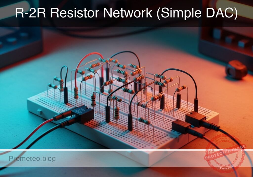
Level: Medium. Construct a resistive ladder to convert 4-bit binary signals into precise analog voltage levels.

Objective and use case

In this session, you will build a 4-bit Digital-to-Analog Converter (DAC) using an R-2R resistor ladder topology. This circuit sums binary weighted inputs to produce an analog output proportional to the digital value.

Why it is useful:
* Audio Synthesis: Used in simple function generators to create sine or triangle waves from digital microcontrollers.
* Video Signals: Historically used in VGA adapters to generate color intensity levels.
* Cost-Effective Control: Allows generating variable control voltages without dedicated DAC chips.
* Signal Processing Education: Demonstrates superposition and Thevenin’s theorem in a practical way.

Expected outcome:
* A stable output voltage (VOUT) that ranges from 0 V to approximately 4.68 V (given a 5 V supply).
* Sixteen distinct voltage steps (from binary 0000 to 1111).
* Linear relationship between the binary input value and the measured analog voltage.

Target audience and level: Electronics students and hobbyists familiar with basic circuit laws.

Materials

  • V1: 5 V DC supply, function: Logic high reference and main power.
  • R1: 10 kΩ resistor, function: Series resistor (R) in ladder spine (Bit 0-1).
  • R2: 10 kΩ resistor, function: Series resistor (R) in ladder spine (Bit 1-2).
  • R3: 10 kΩ resistor, function: Series resistor (R) in ladder spine (Bit 2-3).
  • R4: 20 kΩ resistor, function: Parallel resistor (2R) for Bit 0 (LSB).
  • R5: 20 kΩ resistor, function: Parallel resistor (2R) for Bit 1.
  • R6: 20 kΩ resistor, function: Parallel resistor (2R) for Bit 2.
  • R7: 20 kΩ resistor, function: Parallel resistor (2R) for Bit 3 (MSB).
  • R8: 20 kΩ resistor, function: Termination resistor (2R) connected to Ground.
  • SW1: SPDT switch (or jumper wire), function: Bit 0 input (LSB), switches between VCC and GND.
  • SW2: SPDT switch (or jumper wire), function: Bit 1 input, switches between VCC and GND.
  • SW3: SPDT switch (or jumper wire), function: Bit 2 input, switches between VCC and GND.
  • SW4: SPDT switch (or jumper wire), function: Bit 3 input (MSB), switches between VCC and GND.

Wiring guide

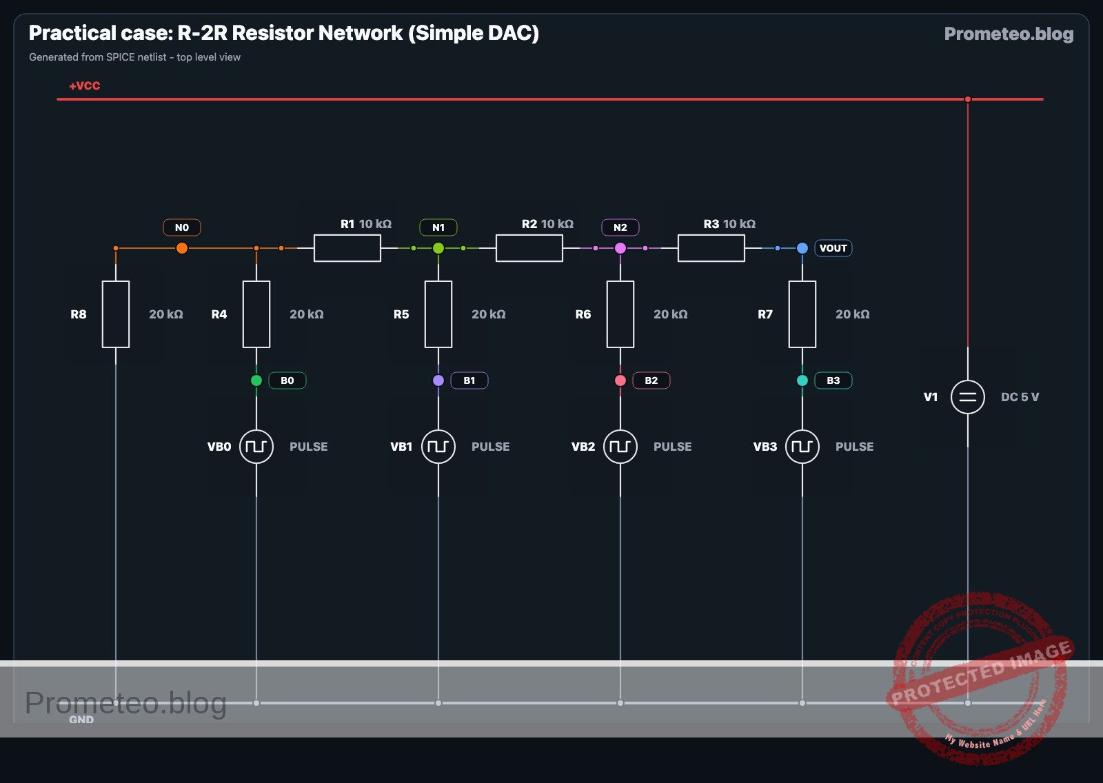
This guide uses node names: VCC (5 V), 0 (GND), B0 (Bit 0 Input), B1 (Bit 1 Input), B2 (Bit 2 Input), B3 (Bit 3 Input), and internal ladder nodes N0, N1, N2. VOUT is the analog output.

  • V1 Connection: Connect V1 positive terminal to VCC and negative to 0.
  • Input Switches (Digital Inputs):
    • SW1: Common to B0, Position 1 to 0, Position 2 to VCC.
    • SW2: Common to B1, Position 1 to 0, Position 2 to VCC.
    • SW3: Common to B2, Position 1 to 0, Position 2 to VCC.
    • SW4: Common to B3, Position 1 to 0, Position 2 to VCC.
  • Ladder «R» Resistors (Spine):
    • R1: Connects between node N0 and node N1.
    • R2: Connects between node N1 and node N2.
    • R3: Connects between node N2 and node VOUT.
  • Ladder «2R» Resistors (Branches):
    • R8 (Termination): Connects between node N0 and 0.
    • R4: Connects between node B0 and node N0.
    • R5: Connects between node B1 and node N1.
    • R6: Connects between node B2 and node N2.
    • R7: Connects between node B3 and node VOUT.
  • Output: Monitor voltage at node VOUT relative to 0.

Conceptual block diagram

Conceptual block diagram — LM358 R-2R Ladder DAC
Quick read: inputs → main block → output (actuator or measurement). This summarizes the ASCII schematic below.

Schematic

[ DIGITAL INPUTS ]              [ R-2R LADDER NETWORK ]                 [ ANALOG OUTPUT ]
(Switches toggle VCC/GND)           (Voltage Summing Logic)

                                                                           +--> [ Multimeter ]
                                                                           |    (Measure V)
[ SW4: Bit 3 (MSB) ] --(High/Low)--> [ R7: 20k (2R) ] --(Bit 3 Weight)---->+--> [ VOUT Node  ]
                                                            ^
                                                            |
                                                     [ R3: 10k (R) ]
                                                            |
[ SW3: Bit 2       ] --(High/Low)--> [ R6: 20k (2R) ] --(Bit 2 Weight)---->+ (Node N2)
                                                            ^
                                                            |
                                                     [ R2: 10k (R) ]
                                                            |
[ SW2: Bit 1       ] --(High/Low)--> [ R5: 20k (2R) ] --(Bit 1 Weight)---->+ (Node N1)
                                                            ^
                                                            |
                                                     [ R1: 10k (R) ]
                                                            |
[ SW1: Bit 0 (LSB) ] --(High/Low)--> [ R4: 20k (2R) ] --(Bit 0 Weight)---->+ (Node N0)
                                                            |
                                                            v
                                                     [ R8: 20k (2R) ]
                                                            |
                                                           GND
Schematic (ASCII)

Electrical diagram

Electrical diagram for case: Practical case: R-2R Resistor Network (Simple DAC)
Generated from the validated SPICE netlist for this case.

🔒 This electrical diagram is premium. With the 7-day pass or the monthly membership you can unlock the complete didactic material and the print-ready PDF pack.🔓 See premium access plans

Measurements and tests

To validate the DAC, you will set the switches to specific binary codes and measure the resulting voltage at VOUT. The formula for the output is:
$VOUT = Vref × ((Decimal Value) / 16)$

  1. Zero Check: Set all switches (SW1-SW4) to 0 (GND). Measure VOUT. It should be exactly 0 V.
  2. LSB Check (Bit 0): Set SW1 to VCC and others to 0 (Binary 0001).
    • Calculation: $5 V × (1/16) = 0.3125 V$.
    • Verify VOUT is approx 0.31 V.
  3. MSB Check (Bit 3): Set SW4 to VCC and others to 0 (Binary 1000).
    • Calculation: $5 V × (8/16) = 2.5 V$.
    • Verify VOUT is approx 2.5 V.
  4. Full Scale Check: Set all switches to VCC (Binary 1111).
    • Calculation: $5 V × (15/16) = 4.6875 V. * Verify VOUT is approx 4.69 V. <! – – SPICE_INSERT_POINT – – > ## Common mistakes and how to avoid them 1. Floating Inputs: Leaving a switch open (disconnected) instead of connecting it to Ground for logic «0». * Solution: R – 2R ladders require inputs to be strictly atV_{ref}$ or $0 V$. Use SPDT switches or verify your jumper wires connect to GND when «off».
  5. Swapping R and 2R: Placing a 10 kΩ resistor where a 20 kΩ is required (or vice versa).
    • Solution: Double-check color codes. 10 kΩ is usually Brown-Black-Orange; 20 kΩ is Red-Black-Orange.
  6. Loading the Output: Connecting a low-impedance load (like a speaker or LED) directly to VOUT.
    • Solution: This circuit has a relatively high output impedance ($R$). Always use an Op-Amp buffer (voltage follower) if you need to drive a load.

SPICE netlist and simulation

Reference SPICE Netlist (ngspice) — excerptFull SPICE netlist (ngspice)

* Practical case: R-2R Resistor Network (Simple DAC)

* --- Power Supply ---
* V1: 5 V DC supply, function: Logic high reference and main power
V1 VCC 0 DC 5

* --- Digital Inputs (Simulated Switches) ---
* Modeled as PULSE voltage sources to strictly simulate user input/switching.
* Generates a binary counting sequence (0000 to 1111) to test the full truth table.
* Logic High = 5V (VCC), Logic Low = 0V (GND).

* SW1 (Bit 0 LSB): Toggles every 100us (Period)
VB0 B0 0 PULSE(0 5 0 1u 1u 50u 100u)

* SW2 (Bit 1): Toggles every 200us (Period)
VB1 B1 0 PULSE(0 5 0 1u 1u 100u 200u)

* SW3 (Bit 2): Toggles every 400us (Period)
VB2 B2 0 PULSE(0 5 0 1u 1u 200u 400u)

* ... (truncated in public view) ...

Copy this content into a .cir file and run with ngspice.

🔒 Part of this section is premium. With the 7-day pass or the monthly membership you can access the full content (materials, wiring, detailed build, validation, troubleshooting, variants and checklist) and download the complete print-ready PDF pack.

* Practical case: R-2R Resistor Network (Simple DAC)

* --- Power Supply ---
* V1: 5 V DC supply, function: Logic high reference and main power
V1 VCC 0 DC 5

* --- Digital Inputs (Simulated Switches) ---
* Modeled as PULSE voltage sources to strictly simulate user input/switching.
* Generates a binary counting sequence (0000 to 1111) to test the full truth table.
* Logic High = 5V (VCC), Logic Low = 0V (GND).

* SW1 (Bit 0 LSB): Toggles every 100us (Period)
VB0 B0 0 PULSE(0 5 0 1u 1u 50u 100u)

* SW2 (Bit 1): Toggles every 200us (Period)
VB1 B1 0 PULSE(0 5 0 1u 1u 100u 200u)

* SW3 (Bit 2): Toggles every 400us (Period)
VB2 B2 0 PULSE(0 5 0 1u 1u 200u 400u)

* SW4 (Bit 3 MSB): Toggles every 800us (Period)
VB3 B3 0 PULSE(0 5 0 1u 1u 400u 800u)

* --- R-2R Ladder Network ---

* -- Spine Resistors (R = 10k) --
* R1: Connects between node N0 and node N1
R1 N0 N1 10k

* R2: Connects between node N1 and node N2
R2 N1 N2 10k

* R3: Connects between node N2 and node VOUT
R3 N2 VOUT 10k

* -- Branch/Termination Resistors (2R = 20k) --
* R8 (Termination): Connects between node N0 and 0 (GND)
R8 N0 0 20k

* R4 (Bit 0 Input): Connects between node B0 and node N0
R4 B0 N0 20k

* R5 (Bit 1 Input): Connects between node B1 and node N1
R5 B1 N1 20k

* R6 (Bit 2 Input): Connects between node B2 and node N2
R6 B2 N2 20k

* R7 (Bit 3 Input - MSB): Connects between node B3 and node VOUT
R7 B3 VOUT 20k

* --- Simulation Directives ---
* Transient analysis to capture the full binary counting sequence (approx 1ms)
.tran 2u 1000u

* --- Output Printing ---
* Monitor the Input Bits and the Analog Output Voltage
.print tran V(B0) V(B1) V(B2) V(B3) V(VOUT)

.op
.end

Simulation Results (Transient Analysis)

Simulation Results (Transient Analysis)
Show raw data table (1384 rows)
Index   time            v(b0)           v(b1)           v(b2)
0	0.000000e+00	0.000000e+00	0.000000e+00	0.000000e+00
1	1.000000e-08	5.000000e-02	5.000000e-02	5.000000e-02
2	2.000000e-08	1.000000e-01	1.000000e-01	1.000000e-01
3	4.000000e-08	2.000000e-01	2.000000e-01	2.000000e-01
4	8.000000e-08	4.000000e-01	4.000000e-01	4.000000e-01
5	1.600000e-07	8.000000e-01	8.000000e-01	8.000000e-01
6	3.200000e-07	1.600000e+00	1.600000e+00	1.600000e+00
7	6.400000e-07	3.200000e+00	3.200000e+00	3.200000e+00
8	1.000000e-06	5.000000e+00	5.000000e+00	5.000000e+00
9	1.064000e-06	5.000000e+00	5.000000e+00	5.000000e+00
10	1.192000e-06	5.000000e+00	5.000000e+00	5.000000e+00
11	1.448000e-06	5.000000e+00	5.000000e+00	5.000000e+00
12	1.960000e-06	5.000000e+00	5.000000e+00	5.000000e+00
13	2.984000e-06	5.000000e+00	5.000000e+00	5.000000e+00
14	4.984000e-06	5.000000e+00	5.000000e+00	5.000000e+00
15	6.984000e-06	5.000000e+00	5.000000e+00	5.000000e+00
16	8.984000e-06	5.000000e+00	5.000000e+00	5.000000e+00
17	1.098400e-05	5.000000e+00	5.000000e+00	5.000000e+00
18	1.298400e-05	5.000000e+00	5.000000e+00	5.000000e+00
19	1.498400e-05	5.000000e+00	5.000000e+00	5.000000e+00
20	1.698400e-05	5.000000e+00	5.000000e+00	5.000000e+00
21	1.898400e-05	5.000000e+00	5.000000e+00	5.000000e+00
22	2.098400e-05	5.000000e+00	5.000000e+00	5.000000e+00
23	2.298400e-05	5.000000e+00	5.000000e+00	5.000000e+00
... (1360 more rows) ...


Reference SPICE netlist (ngspice)

* Practical case: R-2R Resistor Network (Simple DAC)

* --- Power Supply ---
* V1: 5 V DC supply, function: Logic high reference and main power
V1 VCC 0 DC 5

* --- Digital Inputs (Simulated Switches) ---
* Modeled as PULSE voltage sources to strictly simulate user input/switching.
* Generates a binary counting sequence (0000 to 1111) to test the full truth table.
* Logic High = 5V (VCC), Logic Low = 0V (GND).

* SW1 (Bit 0 LSB): Toggles every 100us (Period)
VB0 B0 0 PULSE(0 5 0 1u 1u 50u 100u)

* SW2 (Bit 1): Toggles every 200us (Period)
VB1 B1 0 PULSE(0 5 0 1u 1u 100u 200u)

* SW3 (Bit 2): Toggles every 400us (Period)
VB2 B2 0 PULSE(0 5 0 1u 1u 200u 400u)

* SW4 (Bit 3 MSB): Toggles every 800us (Period)
VB3 B3 0 PULSE(0 5 0 1u 1u 400u 800u)

* --- R-2R Ladder Network ---

* -- Spine Resistors (R = 10k) --
* R1: Connects between node N0 and node N1
R1 N0 N1 10k

* R2: Connects between node N1 and node N2
R2 N1 N2 10k

* R3: Connects between node N2 and node VOUT
R3 N2 VOUT 10k

* -- Branch/Termination Resistors (2R = 20k) --
* R8 (Termination): Connects between node N0 and 0 (GND)
R8 N0 0 20k

* R4 (Bit 0 Input): Connects between node B0 and node N0
R4 B0 N0 20k

* R5 (Bit 1 Input): Connects between node B1 and node N1
R5 B1 N1 20k

* R6 (Bit 2 Input): Connects between node B2 and node N2
R6 B2 N2 20k

* R7 (Bit 3 Input - MSB): Connects between node B3 and node VOUT
R7 B3 VOUT 20k

* --- Simulation Directives ---
* Transient analysis to capture the full binary counting sequence (approx 1ms)
.tran 2u 1000u

* --- Output Printing ---
* Monitor the Input Bits and the Analog Output Voltage
.print tran V(B0) V(B1) V(B2) V(B3) V(VOUT)

.op
.end

Simulation Results (Transient Analysis)

Simulation Results (Transient Analysis)

Troubleshooting

  • Symptom: $V_{OUT}$ is 2.5 V when it should be 1.25 V.
    • Cause: The MSB (Bit 3) might be stuck high, or resistors are swapped.
    • Fix: Check switch continuity and verify resistor placement at node VOUT.
  • Symptom: Output voltages are non-linear or random.
    • Cause: Poor connection on the «spine» resistors (R1, R2, R3).
    • Fix: Re-seat the resistors on the breadboard to ensure the ladder chain is intact.
  • Symptom: Output never reaches near 4.6 V.
    • Cause: Resistor tolerance accumulation or low power supply voltage.
    • Fix: Measure V1 actual voltage. Use 1% tolerance metal film resistors for better precision.

Possible improvements and extensions

  1. 8-Bit Expansion: Add four more stages to the ladder (using more R and 2R resistors) to create an 8-bit DAC with 256 voltage steps.
  2. Active Buffering: Connect VOUT to an LM358 Op-Amp configured as a unity-gain buffer to drive an LED or a small audio speaker safely.

More Practical Cases on Prometeo.blog

Find this product and/or books on this topic on Amazon

Go to Amazon

As an Amazon Associate, I earn from qualifying purchases. If you buy through this link, you help keep this project running.

Quick Quiz

Question 1: What is the primary function of the circuit described in the text?


Question 2: Which resistor topology is used to build the DAC in this session?


Question 3: What is the expected maximum output voltage (V_OUT) given a 5 V supply?


Question 4: How many distinct voltage steps can a 4-bit DAC produce?


Question 5: Which of the following is a historical use case mentioned for this type of circuit?


Question 6: What relationship is expected between the binary input value and the measured analog voltage?


Question 7: What theoretical concepts does this project demonstrate practically?


Question 8: Why is the R-2R ladder considered a cost-effective control method?


Question 9: Which application involves creating sine or triangle waves from digital microcontrollers?


Question 10: Who is the target audience for this project?


Carlos Núñez Zorrilla
Electronics & Computer Engineer

Telecommunications Electronics Engineer and Computer Engineer (official degrees in Spain).

Follow me:


Practical case: Unbalanced Wheatstone Bridge

Unbalanced Wheatstone Bridge prototype (Maker Style)

Level: Medium. Analyze differential voltage variation in a resistive bridge by modifying a sensor.

Objective and use case

You will build a Wheatstone bridge circuit using three fixed resistors and one variable resistor to simulate a resistive sensor. This circuit converts a change in resistance into a measurable differential voltage output.

Why it is useful:
* Precision Sensing: Used in load cells (weighing scales) and strain gauges where resistance changes are minute.
* Temperature Measurement: Fundamental for reading RTDs (Resistance Temperature Detectors) and thermistors.
* Zero Calibration: Allows systems to establish a «null point» (0 V output) to cancel out offset errors before taking measurements.
* Small Signal Detection: Filters out power supply noise common to both legs of the bridge (Common Mode Rejection).

Expected outcome:
* Balanced State: When the variable resistor matches the ratio of the fixed arm, the differential voltage (VAB) reads exactly 0 V.
* Unbalanced State: As the resistance changes, VAB becomes positive or negative depending on the direction of the change.
* Sensitivity: You will observe the non-linear relationship between the resistance change (\Delta R) and the output voltage (VOUT).

Target audience and level: Electronics students and hobbyists familiar with Ohm’s Law (Medium).

Materials

  • V1: 5 V DC voltage source, function: main power supply.
  • R1: 1 kΩ resistor, function: upper reference arm.
  • R2: 1 kΩ resistor, function: lower reference arm.
  • R3: 1 kΩ resistor, function: upper measurement arm.
  • R4: 2 kΩ potentiometer (linear), function: variable resistor (simulating a sensor like a thermistor or strain gauge).

Wiring guide

This circuit consists of two parallel voltage dividers connected to a common source. The output is taken differentially between the center points of these dividers.

  • V1 connects between node VCC (positive) and node 0 (GND).
  • R1 connects between node VCC and node VA (Reference Point).
  • R2 connects between node VA and node 0.
  • R3 connects between node VCC and node VB (Measurement Point).
  • R4 connects between node VB and node 0.
  • Measurement: The output VOUT is measured between node VA and node VB.

Conceptual block diagram

Conceptual block diagram — Unbalanced Wheatstone Bridge
Quick read: inputs → main block → output (actuator or measurement). This summarizes the ASCII schematic below.

Schematic

[ SOURCE ]                     [ BRIDGE PROCESSING ]                     [ OUTPUT ]

                               +-----------------------------+
                               |   Reference Divider (Left)  |
                            +->|  (Fixed Ratio: R1 / R2)     |--(Node VA)-->+
                            |  |  [ R1: 1 kΩ ] + [ R2: 1 kΩ ]  |              |
                            |  +-----------------------------+              |
                            |                                               v
[ V1: 5 V DC ] --(Supply)--> +                                          [ V_OUT ]
                            |                                          (Differential)
                            |  +-----------------------------+         ( VA - VB )
                            |  |  Measurement Divider (Right)|              ^
                            +->|  (Variable Ratio: R3 / R4)  |--(Node VB)-->+
                               |  [ R3: 1 kΩ ] + [ R4: Pot ]  |
                               +-----------------------------+
Schematic (ASCII)

Electrical diagram

Electrical diagram for case: Unbalanced Wheatstone Bridge
Generated from the validated SPICE netlist for this case.

🔒 This electrical diagram is premium. With the 7-day pass or the monthly membership you can unlock the complete didactic material and the print-ready PDF pack.🔓 See premium access plans

Measurements and tests

Follow these steps to validate the bridge operation using a voltmeter or multimeter.

  1. Setup: Power the circuit with 5 V. Set your multimeter to measure DC Voltage in the 20 V or 2 V range.
  2. Verify Reference: Measure the voltage between VA and 0 (GND). With R1 and R2 being equal (1 kΩ), this should be stable at exactly 2.5 V.
  3. Find the Null Point: Connect the multimeter probes between VA (red probe) and VB (black probe). Adjust potentiometer R4 until the multimeter reads 0.00 V.
    • Observation: At this point, the bridge is balanced (R1 / R2 = R3 / R4). R4 should be approximately 1 kΩ.
  4. Simulate Sensor Increase: Increase the resistance of R4.
    • Observation: The voltage at VB rises. The differential reading (VA – VB) will become negative (assuming Red probe on A, Black on B).
  5. Simulate Sensor Decrease: Decrease the resistance of R4 below 1 kΩ.
    • Observation: The voltage at VB drops. The differential reading will become positive.

SPICE netlist and simulation

Reference SPICE Netlist (ngspice) — excerptFull SPICE netlist (ngspice)

* Practical case: Unbalanced Wheatstone Bridge

* --- Power Supply ---
* V1: 5 V DC voltage source, main power supply
V1 VCC 0 DC 5

* --- Reference Arm (Left) ---
* R1: 1 kΩ, upper reference arm
R1 VCC VA 1k

* R2: 1 kΩ, lower reference arm
R2 VA 0 1k

* --- Measurement Arm (Right) ---
* R3: 1 kΩ, upper measurement arm
R3 VCC VB 1k

* R4: 2 kΩ potentiometer (simulating sensor), lower measurement arm
* Connected between VB and 0. Set to 2k to demonstrate unbalanced state.
R4 VB 0 2k
* ... (truncated in public view) ...

Copy this content into a .cir file and run with ngspice.

🔒 Part of this section is premium. With the 7-day pass or the monthly membership you can access the full content (materials, wiring, detailed build, validation, troubleshooting, variants and checklist) and download the complete print-ready PDF pack.

* Practical case: Unbalanced Wheatstone Bridge

* --- Power Supply ---
* V1: 5 V DC voltage source, main power supply
V1 VCC 0 DC 5

* --- Reference Arm (Left) ---
* R1: 1 kΩ, upper reference arm
R1 VCC VA 1k

* R2: 1 kΩ, lower reference arm
R2 VA 0 1k

* --- Measurement Arm (Right) ---
* R3: 1 kΩ, upper measurement arm
R3 VCC VB 1k

* R4: 2 kΩ potentiometer (simulating sensor), lower measurement arm
* Connected between VB and 0. Set to 2k to demonstrate unbalanced state.
R4 VB 0 2k

* --- Simulation Setup ---
* Calculate DC operating point
.op

* Transient analysis (10ms duration to verify stability)
.tran 100u 10m

* --- Output Directives ---
* Monitor Supply, Reference Voltage (VA), and Sensor Voltage (VB)
* Differential Output VOUT = V(VA) - V(VB)
.print tran V(VCC) V(VA) V(VB)

.end

Simulation Results (Transient Analysis)

Simulation Results (Transient Analysis)
Show raw data table (108 rows)
Index   time            v(vcc)          v(va)           v(vb)
0	0.000000e+00	5.000000e+00	2.500000e+00	3.333333e+00
1	1.000000e-06	5.000000e+00	2.500000e+00	3.333333e+00
2	2.000000e-06	5.000000e+00	2.500000e+00	3.333333e+00
3	4.000000e-06	5.000000e+00	2.500000e+00	3.333333e+00
4	8.000000e-06	5.000000e+00	2.500000e+00	3.333333e+00
5	1.600000e-05	5.000000e+00	2.500000e+00	3.333333e+00
6	3.200000e-05	5.000000e+00	2.500000e+00	3.333333e+00
7	6.400000e-05	5.000000e+00	2.500000e+00	3.333333e+00
8	1.280000e-04	5.000000e+00	2.500000e+00	3.333333e+00
9	2.280000e-04	5.000000e+00	2.500000e+00	3.333333e+00
10	3.280000e-04	5.000000e+00	2.500000e+00	3.333333e+00
11	4.280000e-04	5.000000e+00	2.500000e+00	3.333333e+00
12	5.280000e-04	5.000000e+00	2.500000e+00	3.333333e+00
13	6.280000e-04	5.000000e+00	2.500000e+00	3.333333e+00
14	7.280000e-04	5.000000e+00	2.500000e+00	3.333333e+00
15	8.280000e-04	5.000000e+00	2.500000e+00	3.333333e+00
16	9.280000e-04	5.000000e+00	2.500000e+00	3.333333e+00
17	1.028000e-03	5.000000e+00	2.500000e+00	3.333333e+00
18	1.128000e-03	5.000000e+00	2.500000e+00	3.333333e+00
19	1.228000e-03	5.000000e+00	2.500000e+00	3.333333e+00
20	1.328000e-03	5.000000e+00	2.500000e+00	3.333333e+00
21	1.428000e-03	5.000000e+00	2.500000e+00	3.333333e+00
22	1.528000e-03	5.000000e+00	2.500000e+00	3.333333e+00
23	1.628000e-03	5.000000e+00	2.500000e+00	3.333333e+00
... (84 more rows) ...


Reference SPICE netlist (ngspice)

* Practical case: Unbalanced Wheatstone Bridge

* --- Power Supply ---
* V1: 5 V DC voltage source, main power supply
V1 VCC 0 DC 5

* --- Reference Arm (Left) ---
* R1: 1 kΩ, upper reference arm
R1 VCC VA 1k

* R2: 1 kΩ, lower reference arm
R2 VA 0 1k

* --- Measurement Arm (Right) ---
* R3: 1 kΩ, upper measurement arm
R3 VCC VB 1k

* R4: 2 kΩ potentiometer (simulating sensor), lower measurement arm
* Connected between VB and 0. Set to 2k to demonstrate unbalanced state.
R4 VB 0 2k

* --- Simulation Setup ---
* Calculate DC operating point
.op

* Transient analysis (10ms duration to verify stability)
.tran 100u 10m

* --- Output Directives ---
* Monitor Supply, Reference Voltage (VA), and Sensor Voltage (VB)
* Differential Output VOUT = V(VA) - V(VB)
.print tran V(VCC) V(VA) V(VB)

.end

Simulation Results (Transient Analysis)

Simulation Results (Transient Analysis)

Common mistakes and how to avoid them

  1. Measuring relative to Ground: Students often measure VA to GND and VB to GND separately. While valid, the bridge is designed to be measured differentially (VA to VB) directly.
    • Solution: Place the voltmeter probes directly across the bridge midpoints.
  2. Using low-tolerance resistors: If R1 and R2 have high tolerance (e.g., 10%), the reference voltage VA will not be exactly VCC/2, making the null point hard to calculate.
    • Solution: Use 1% metal film resistors for R1, R2, and R3 for precision.
  3. Loading the bridge: Connecting a low-impedance load (like a motor or a low-resistance speaker) directly between VA and VB.
    • Solution: The bridge is for signal measurement, not power. Always connect the output nodes to a high-impedance input, such as an Op-Amp or microcontroller ADC.

Troubleshooting

  • Symptom: Output voltage is always 0 V regardless of potentiometer position.
    • Cause: Power supply is off or there is a short circuit between VA and VB.
    • Fix: Check V1 connections and ensure the two legs of the bridge are not shorted together.
  • Symptom: Cannot reach 0 V (Null point) output.
    • Cause: The fixed resistor R3 is significantly different from the range of potentiometer R4.
    • Fix: Ensure R4’s range includes the value of R3 (e.g., if R3 is 1 kΩ, R4 must be capable of reaching 1 kΩ).
  • Symptom: Readings are unstable or «jittery».
    • Cause: Noisy potentiometer wiper or loose breadboard contacts.
    • Fix: Replace the potentiometer or ensure solid connections on the breadboard.

Possible improvements and extensions

  1. Instrumentation Amplifier: Feed nodes VA and VB into an instrumentation amplifier (like the AD620) to amplify the small differential voltage for a microcontroller to read.
  2. Physical Sensor: Replace R4 with a photoresistor (LDR) or a thermistor (NTC). Observe how light or temperature changes the bridge balance.

More Practical Cases on Prometeo.blog

Find this product and/or books on this topic on Amazon

Go to Amazon

As an Amazon Associate, I earn from qualifying purchases. If you buy through this link, you help keep this project running.

Quick Quiz

Question 1: What is the primary function of the Wheatstone bridge circuit described in the objective?


Question 2: Which component in the circuit is used to simulate a resistive sensor like a thermistor or strain gauge?


Question 3: What is the expected differential voltage (V_AB) when the bridge is in a 'Balanced State'?


Question 4: Why is 'Zero Calibration' mentioned as a useful feature of this circuit?


Question 5: In the context of 'Small Signal Detection', what does the bridge circuit help filter out?


Question 6: What happens to the differential voltage (V_AB) in an 'Unbalanced State'?


Question 7: Which application is explicitly listed as a use case for precision sensing with this circuit?


Question 8: What relationship is generally observed between the resistance change and the output voltage in a Wheatstone bridge?


Question 9: What is the role of the component labeled V1 in the context of this circuit?


Question 10: Which specific type of temperature sensor is mentioned as fundamental for reading with this circuit?


Carlos Núñez Zorrilla
Electronics & Computer Engineer

Telecommunications Electronics Engineer and Computer Engineer (official degrees in Spain).

Follow me:


Practical case: Empty Tank Level Indicator

Empty Tank Level Indicator prototype (Maker Style)

Level: Medium. Design a logic circuit that alerts the user when a water sensor stops detecting liquid using a NOT gate.

Objective and use case

In this case, you will build a monitoring circuit using a 74HC04 inverter that illuminates a red LED when a tank’s liquid level drops below a critical point.

  • Prevents pump damage: Stops water pumps from running dry in hydroponic systems.
  • Household safety: Alerts when rooftop reserve tanks are empty.
  • Industrial maintenance: Visual flag for coolant refill requirements.

Expected outcome:
* Water Present: The sensor is open (Logic 1 input) $\rightarrow$ LED remains OFF.
* Tank Empty: The sensor closes (Logic 0 input) $\rightarrow$ LED turns ON.
* Logic Level: $V_{in} \approx 0\text{ V}$ activates the alert; $V_{in} \approx 5\text{ V}$ indicates normal status.

Target audience: Electronics students and hobbyists familiar with basic digital logic.

Materials

  • V1: 5 V DC power supply, function: main circuit power
  • U1: 74HC04 Hex Inverter IC, function: logic inversion
  • S1: Float switch (SPST, configured to Close when Empty), function: liquid level sensor
  • R1: 10 kΩ resistor, function: pull-up for sensor signal
  • R2: 330 Ω resistor, function: LED current limiting
  • D1: Red LED, function: visual empty alert
  • C1: 100 nF ceramic capacitor, function: power supply decoupling

Pin-out of the IC used

Selected Chip: 74HC04 (Hex Inverter)

Pin Name Logic function Connection in this case
1 1A Input Connected to Sensor Node (SENSE_IN)
2 1Y Output Connected to LED circuit (ALERT_OUT)
7 GND Ground Connected to GND (0 V)
14 VCC Power Connected to 5 V Supply

Wiring guide

  • V1 connects between node VCC and node GND.
  • C1 connects between node VCC and node GND (placed physically close to U1).
  • R1 connects between node VCC and node SENSE_IN.
  • S1 connects between node SENSE_IN and node GND.
  • U1 pin 1 connects to node SENSE_IN.
  • U1 pin 2 connects to node ALERT_OUT.
  • U1 pin 14 connects to VCC; pin 7 connects to GND.
  • R2 connects between node ALERT_OUT and node LED_ANODE.
  • D1 connects between node LED_ANODE (Anode) and node GND (Cathode).

Conceptual block diagram

Conceptual block diagram — 74HC04 NOT gate

Schematic

[ INPUT / SENSOR ]                 [ LOGIC PROCESSING ]                 [ OUTPUT / ALERT ]

[ VCC 5V ] --> [ R1: 10k ] --+
               (Pull-Up)     |
                             |
                             V
                        (SENSE_IN) ---->+------------------+
                        (Pin 1)         |    U1: 74HC04    |
                             ^          |   Hex Inverter   |--(ALERT_OUT)--> [ R2: 330R ] --> [ D1: Red LED ] --> GND
                             |          |   (Pin 1 -> 2)   |  (Pin 2)        (Limiting)       (Anode/Cathode)
[ GND 0V ] --> [ S1: Float ]-+          +------------------+
               (Switch)                           ^
                                                  |
                                            [ C1: 100nF ]
                                            (Decoupling)
                                            (VCC / GND)
Schematic (ASCII)

Truth table

Water State Sensor Switch (S1) Input Voltage (Pin 1) Logic Input Output Voltage (Pin 2) LED State
Full OPEN 5 V (via Pull-up) 1 0 V OFF
Empty CLOSED 0 V (connected to GND) 0 5 V ON

Measurements and tests

  1. Supply Check: Measure voltage between VCC and GND. Ensure it is stable at 5 V.
  2. Full Tank Simulation: Manually lift the float (ensure S1 is OPEN). Measure voltage at SENSE_IN. It should be $\approx 5\text{ V}$. Verify LED is OFF.
  3. Empty Tank Simulation: Drop the float (ensure S1 is CLOSED). Measure voltage at SENSE_IN. It should be $\approx 0\text{ V}$.
  4. Logic Output: While S1 is closed (Empty), measure voltage at ALERT_OUT. It should be $\approx 5\text{ V}$.
  5. Current Draw: Measure the current through D1 ($I_{led}$) when ON. It should be approximately 10–12 mA depending on the specific LED voltage drop.

SPICE netlist and simulation

Reference SPICE Netlist (ngspice) — excerptFull SPICE netlist (ngspice)

* Practical case: Empty Tank Level Indicator

* ==============================================================================
* BILL OF MATERIALS & COMPONENTS
* ==============================================================================

* --- Power Supply ---
* V1: 5 V DC power supply
V1 VCC 0 DC 5

* --- Decoupling ---
* C1: 100 nF ceramic capacitor (Power supply decoupling)
C1 VCC 0 100n

* --- Sensor Input Section ---
* R1: 10 kΩ resistor (Pull-up for sensor signal)
R1 VCC SENSE_IN 10k

* S1: Float switch (SPST)
* Wiring: Connects between node SENSE_IN and node GND.
* ... (truncated in public view) ...

Copy this content into a .cir file and run with ngspice.

🔒 Part of this section is premium. With the 7-day pass or the monthly membership you can access the full content (materials, wiring, detailed build, validation, troubleshooting, variants and checklist) and download the complete print-ready PDF pack.

* Practical case: Empty Tank Level Indicator

* ==============================================================================
* BILL OF MATERIALS & COMPONENTS
* ==============================================================================

* --- Power Supply ---
* V1: 5 V DC power supply
V1 VCC 0 DC 5

* --- Decoupling ---
* C1: 100 nF ceramic capacitor (Power supply decoupling)
C1 VCC 0 100n

* --- Sensor Input Section ---
* R1: 10 kΩ resistor (Pull-up for sensor signal)
R1 VCC SENSE_IN 10k

* S1: Float switch (SPST)
* Wiring: Connects between node SENSE_IN and node GND.
* Simulation: Modeled as a Voltage Controlled Switch (SW).
* Logic: 
*   - Tank Full (Float Up) -> Switch Open -> SENSE_IN pulled to VCC.
*   - Tank Empty (Float Down) -> Switch Closed -> SENSE_IN pulled to GND.
* Control Source V_FLOAT_ACT simulates the float movement.
*   - 0V = Float Up (Full)
*   - 5V = Float Down (Empty)
S1 SENSE_IN 0 FLOAT_CTRL 0 SW_FLOAT
.model SW_FLOAT SW(Vt=2.5 Ron=0.1 Roff=10Meg)

* Stimulus: Float starts Up (Full), drops to Down (Empty) at 50us, returns at 200us.
V_FLOAT_ACT FLOAT_CTRL 0 PULSE(0 5 50u 1u 1u 150u 400u)

* --- Logic Processing ---
* U1: 74HC04 Hex Inverter
* Wiring Guide: Pin 1 (In) -> SENSE_IN, Pin 2 (Out) -> ALERT_OUT
* Power: Pin 14 -> VCC, Pin 7 -> GND
* Implemented as a subcircuit to strictly map pins.
XU1 SENSE_IN ALERT_OUT 0 VCC 74HC04_GATE

* Subcircuit definition for one gate of 74HC04
.subckt 74HC04_GATE IN OUT GND VCC
    * Behavioral voltage source for robust logic inversion
    * Uses sigmoid function for convergence: Vout = VCC if Vin < 2.5V
    B1 OUT GND V = V(VCC) * (1 / (1 + exp(50 * (V(IN) - 2.5))))
.ends

* --- Output Alert ---
* R2: 330 Ω resistor (LED current limiting)
R2 ALERT_OUT LED_ANODE 330

* D1: Red LED (Visual empty alert)
* Wiring: Anode -> LED_ANODE, Cathode -> GND
D1 LED_ANODE 0 LED_RED
.model LED_RED D(IS=1e-14 N=2 RS=5 BV=5 IBV=10u CJO=40p)

* ==============================================================================
* ANALYSIS COMMANDS
* ==============================================================================

* Operating Point Analysis
.op

* Transient Analysis
* Run for 500us to capture the float switch activation cycle
.tran 1u 500u

* Output Printing
* Monitor Sensor Input, Inverter Output, and LED Voltage
.print tran V(SENSE_IN) V(ALERT_OUT) V(LED_ANODE) V(FLOAT_CTRL)

.end

Simulation Results (Transient Analysis)

Simulation Results (Transient Analysis)
Show raw data table (1190 rows)
Index   time            v(sense_in)     v(alert_out)    v(led_anode)
0	0.000000e+00	4.995005e+00	3.316079e-54	-1.70080e-28
1	1.000000e-08	4.995005e+00	3.316079e-54	-9.73961e-29
2	2.000000e-08	4.995005e+00	3.316079e-54	-1.41516e-29
3	4.000000e-08	4.995005e+00	3.316079e-54	8.723601e-29
4	8.000000e-08	4.995005e+00	3.316079e-54	1.163518e-28
5	1.600000e-07	4.995005e+00	3.316079e-54	4.380930e-29
6	3.200000e-07	4.995005e+00	3.316079e-54	-1.45299e-29
7	6.400000e-07	4.995005e+00	3.316079e-54	-1.01395e-29
8	1.280000e-06	4.995005e+00	3.316079e-54	-5.46095e-32
9	2.280000e-06	4.995005e+00	3.316079e-54	4.098577e-31
10	3.280000e-06	4.995005e+00	3.316079e-54	2.282032e-32
11	4.280000e-06	4.995005e+00	3.316079e-54	-9.50625e-33
12	5.280000e-06	4.995005e+00	3.316079e-54	-1.09186e-33
13	6.280000e-06	4.995005e+00	3.316079e-54	1.911218e-34
14	7.280000e-06	4.995005e+00	3.316079e-54	3.847480e-35
15	8.280000e-06	4.995005e+00	3.316079e-54	-2.97995e-36
16	9.280000e-06	4.995005e+00	3.316079e-54	-1.15977e-36
17	1.028000e-05	4.995005e+00	3.316079e-54	1.723722e-38
18	1.128000e-05	4.995005e+00	3.316079e-54	3.117034e-38
19	1.228000e-05	4.995005e+00	3.316079e-54	1.177223e-39
20	1.328000e-05	4.995005e+00	3.316079e-54	-7.52109e-40
21	1.428000e-05	4.995005e+00	3.316079e-54	-6.99870e-41
22	1.528000e-05	4.995005e+00	3.316079e-54	1.597704e-41
23	1.628000e-05	4.995005e+00	3.316079e-54	2.660714e-42
... (1166 more rows) ...

Common mistakes and how to avoid them

  1. Leaving inputs floating: Even though we only use one gate (Pin 1/2), unused inputs on CMOS chips (pins 3, 5, 9, 11, 13) should be tied to GND or VCC to prevent oscillation and excess power consumption.
  2. Incorrect Pull-up wiring: Connecting the resistor in series with the input instead of as a pull-up to VCC. Ensure R1 goes strictly to 5V.
  3. Sensor Logic inversion: Using a sensor that is Open when Empty without changing the circuit logic. This would cause the light to be ON when the tank is full. Ensure the mechanical action matches the truth table.

Troubleshooting

  • LED is always ON: Check if S1 is stuck in the Closed position or if pin 1 is shorted to ground.
  • LED never turns ON: Check if the float switch is actually closing the circuit to ground. Measure resistance across S1 terminals while moving the float.
  • Chip gets hot: Check for short circuits at the output or if VCC/GND are reversed (Pins 14 and 7).
  • LED flickers: The liquid might be turbulent. Add a capacitor (e.g., 10 µF) in parallel with S1 to create a hardware debounce delay.

Possible improvements and extensions

  1. Audio Alert: Add a 5V active buzzer in parallel with the LED/Resistor combo to provide an audible alarm when the tank is empty.
  2. Hysteresis: Replace the 74HC04 with a 74HC14 (Schmitt Trigger Inverter). This prevents the LED from jittering if the water level is right at the switching threshold.

More Practical Cases on Prometeo.blog

Quick Quiz

Question 1: What is the primary function of the circuit described in the objective?


Question 2: Which specific logic gate IC is used to perform the inversion in this circuit?


Question 3: How does the LED behave when the water sensor detects liquid (Logic 1 input)?


Question 4: What is the state of the sensor input when the tank is empty according to the expected outcome?


Question 5: What is the primary role of the 10 kΩ resistor (R1) in this specific circuit design?


Question 6: Which component serves as the visual indicator for the alert?


Question 7: What voltage level (Vin) corresponds to a 'normal status' where the alert is inactive?


Question 8: What is a listed practical application for this circuit?


Question 9: The float switch (S1) is configured to do what when the tank is empty?


Question 10: What logic level activates the alert (turns the LED ON)?


Carlos Núñez Zorrilla
Electronics & Computer Engineer

Telecommunications Electronics Engineer and Computer Engineer (official degrees in Spain).

Follow me:


Practical case: Production Line Fault Monitoring

Production Line Fault Monitoring prototype (Maker Style)

Level: Medium. Implement a safety system that stops a conveyor belt if either the temperature sensor OR the jam sensor detects an anomaly.

Objective and use case

You will build a logic control circuit using an OR gate to combine signals from two distinct safety sensors (Temperature and Optical Jam). When either sensor detects a fault (Logic High), the system will output an active signal to trigger an indicator or stop mechanism.

Why it is useful:
* Industrial Safety: Prevents machinery from operating under dangerous conditions.
* Equipment Protection: Stops motors immediately if they overheat to prevent permanent damage.
* Process Efficiency: Detects physical jams on conveyor belts automatically, reducing waste.
* Redundancy: Allows multiple different error types to trigger the same emergency stop routine.

Expected outcome:
* System Standby: When both sensors are Low (0V), the output LED is OFF.
* Temperature Fault: If the temperature sensor triggers (High/5V), the LED turns ON.
* Jam Fault: If the jam sensor triggers (High/5V), the LED turns ON.
* Critical Failure: If both sensors trigger simultaneously, the LED remains ON.

Target audience and level: Electronics students and hobbyists, Level Medium.

Materials

  • V1: 5 V DC power supply, function: Main circuit power.
  • U1: 74HC32, function: Quad 2-input OR gate IC.
  • S1: SPST Toggle Switch, function: Simulates Temperature Sensor (Open=Normal, Closed=Overheat).
  • S2: SPST Toggle Switch, function: Simulates Jam Sensor (Open=Clear, Closed=Jam).
  • R1: 10 kΩ resistor, function: Pull-down for Temperature Input.
  • R2: 10 kΩ resistor, function: Pull-down for Jam Input.
  • R3: 330 Ω resistor, function: Current limiting for indicator LED.
  • D1: Red LED, function: Visual Fault Indicator.

Pin-out of the IC used

Selected Chip: 74HC32 (Quad 2-Input OR Gate)

Pin Name Logic function Connection in this case
1 1A Input A Connected to Temperature Sensor (S1)
2 1B Input B Connected to Jam Sensor (S2)
3 1Y Output Connected to LED driver (R3 + D1)
7 GND Ground Connected to Power Supply Negative (0V)
14 VCC Power (+) Connected to Power Supply Positive (5V)

Wiring guide

  • VCC: Connect V1 positive terminal to U1 pin 14.
  • 0 (GND): Connect V1 negative terminal to U1 pin 7.
  • VA (Temp Signal): Connect S1 terminal 2 to U1 pin 1.
  • VA (Temp Signal): Connect R1 between U1 pin 1 and 0.
  • VCC: Connect S1 terminal 1 to VCC.
  • VB (Jam Signal): Connect S2 terminal 2 to U1 pin 2.
  • VB (Jam Signal): Connect R2 between U1 pin 2 and 0.
  • VCC: Connect S2 terminal 1 to VCC.
  • V_OUT: Connect U1 pin 3 to R3 terminal 1.
  • LED_NODE: Connect R3 terminal 2 to D1 Anode.
  • 0 (GND): Connect D1 Cathode to 0.

Conceptual block diagram

Conceptual block diagram — 74HC32 OR gate

Schematic

Title: Production Line Fault Monitoring (OR Logic)

      [ INPUT SENSORS ]                       [ LOGIC PROCESSING ]                 [ VISUAL OUTPUT ]

                                                 (Pin 14: VCC)
                                                       |
                                                       v
[ VCC ] --> [ S1: Temp Switch ] --+--(Pin 1)-->+---------------+
                                  |            |               |
                             [ R1: 10k ]       |   U1: 74HC32  |
                                  |            |   (OR Gate)   |--(Pin 3)--> [ R3: 330 ] --> [ D1: LED ] --> [ GND ]
                               [ GND ]         |               |
                                               |               |
[ VCC ] --> [ S2: Jam Switch  ] --+--(Pin 2)-->+---------------+
                                  |                    ^
                             [ R2: 10k ]               |
                                  |               (Pin 7: GND)
                               [ GND ]
Schematic (ASCII)

Electrical diagram

Electrical diagram for case: Practical case: Production Line Fault Monitoring
Generated from the validated SPICE netlist for this case.

🔒 This electrical diagram is premium. With the 7-day pass or the monthly membership you can unlock the complete didactic material and the print-ready PDF pack.🔓 See premium access plans

Truth table

This circuit utilizes positive logic (Active High).

Sensor A (Temp) Sensor B (Jam) Output (Fault Indicator) LED State
Low (0) Low (0) Low (0) OFF
Low (0) High (1) High (1) ON
High (1) Low (0) High (1) ON
High (1) High (1) High (1) ON

Measurements and tests

  1. Standby Check: Ensure both switches S1 and S2 are open. Measure voltage at U1 Pin 3 relative to GND. It should be ~0 V. LED should be OFF.
  2. Temperature Fault Simulation: Close S1 while keeping S2 open. Measure voltage at Pin 1 (Input A). It should be 5 V. The Output Pin 3 should go to High (~5 V) and the LED must light up.
  3. Jam Fault Simulation: Open S1 and close S2. Measure voltage at Pin 2 (Input B). It should be 5 V. The LED must light up.
  4. Simultaneous Fault: Close both S1 and S2. The LED must remain ON.

SPICE netlist and simulation

Reference SPICE Netlist (ngspice) — excerptFull SPICE netlist (ngspice)

* Practical case: Production Line Fault Monitoring

* --- Component Models ---
* Generic Red LED Model
.model DLED D (IS=1e-14 N=2 RS=10 BV=5 IBV=10u CJO=10p)

* --- Subcircuits ---
* 74HC32 Quad 2-input OR Gate
* Pinout: 1=InputA, 2=InputB, 3=Output, 7=GND, 14=VCC
* Implemented using a robust behavioral source with continuous functions
.subckt 74HC32 1 2 3 7 14
* Logic: Output = VCC if (A > 2.5V OR B > 2.5V)
* Using sigmoid function for smooth convergence: S(x) = 1/(1+exp(-k*(x-thresh)))
* max(V(1), V(2)) selects the higher voltage to compare against threshold (2.5V)
B_OR 3 7 V = V(14) * (1 / (1 + exp(-20 * (max(V(1), V(2)) - 2.5))))
.ends

* --- Main Power Supply ---
* V1: 5V DC Supply
* Wiring: Positive -> Node 14 (VCC), Negative -> Node 0 (GND)
V1 14 0 DC 5

* --- Input Sensors (Simulated Switches) ---
* S1: Temperature Sensor Switch
* Wiring: Connects VCC to VA (Pin 1). Modeled as Pulse Source to simulate toggling.
* Logic Sequence: High (Overheat) / Low (Normal)
VS1 VA 0 PULSE(0 5 0 1u 1u 200u 400u)

* S2: Jam Sensor Switch
* Wiring: Connects VCC to VB (Pin 2). Modeled as Pulse Source with faster period.
* ... (truncated in public view) ...

Copy this content into a .cir file and run with ngspice.

🔒 Part of this section is premium. With the 7-day pass or the monthly membership you can access the full content (materials, wiring, detailed build, validation, troubleshooting, variants and checklist) and download the complete print-ready PDF pack.

* Practical case: Production Line Fault Monitoring

* --- Component Models ---
* Generic Red LED Model
.model DLED D (IS=1e-14 N=2 RS=10 BV=5 IBV=10u CJO=10p)

* --- Subcircuits ---
* 74HC32 Quad 2-input OR Gate
* Pinout: 1=InputA, 2=InputB, 3=Output, 7=GND, 14=VCC
* Implemented using a robust behavioral source with continuous functions
.subckt 74HC32 1 2 3 7 14
* Logic: Output = VCC if (A > 2.5V OR B > 2.5V)
* Using sigmoid function for smooth convergence: S(x) = 1/(1+exp(-k*(x-thresh)))
* max(V(1), V(2)) selects the higher voltage to compare against threshold (2.5V)
B_OR 3 7 V = V(14) * (1 / (1 + exp(-20 * (max(V(1), V(2)) - 2.5))))
.ends

* --- Main Power Supply ---
* V1: 5V DC Supply
* Wiring: Positive -> Node 14 (VCC), Negative -> Node 0 (GND)
V1 14 0 DC 5

* --- Input Sensors (Simulated Switches) ---
* S1: Temperature Sensor Switch
* Wiring: Connects VCC to VA (Pin 1). Modeled as Pulse Source to simulate toggling.
* Logic Sequence: High (Overheat) / Low (Normal)
VS1 VA 0 PULSE(0 5 0 1u 1u 200u 400u)

* S2: Jam Sensor Switch
* Wiring: Connects VCC to VB (Pin 2). Modeled as Pulse Source with faster period.
* Logic Sequence: High (Jam) / Low (Clear)
VS2 VB 0 PULSE(0 5 0 1u 1u 100u 200u)

* --- Pull-down Resistors ---
* R1: 10k Pull-down for Temp Input
R1 VA 0 10k
* R2: 10k Pull-down for Jam Input
R2 VB 0 10k

* --- Logic IC U1 ---
* U1: 74HC32 Quad OR Gate
* Connections per wiring guide:
* Pin 1 (A) -> VA
* Pin 2 (B) -> VB
* Pin 3 (Y) -> V_OUT
* Pin 7 (GND) -> 0
* Pin 14 (VCC) -> 14
XU1 VA VB V_OUT 0 14 74HC32

* --- Output Indicator ---
* R3: 330 Ohm Current Limiting Resistor
R3 V_OUT LED_NODE 330

* D1: Red LED Visual Indicator
* Anode -> LED_NODE, Cathode -> GND
D1 LED_NODE 0 DLED

* --- Analysis Directives ---
* Transient analysis to capture truth table states (00, 01, 10, 11)
.tran 1u 400u

* Print required voltages for verification
.print tran V(VA) V(VB) V(V_OUT) V(LED_NODE)

* Calculate DC operating point
.op

.end

Simulation Results (Transient Analysis)

Simulation Results (Transient Analysis)
Show raw data table (906 rows)
Index   time            v(va)           v(vb)           v(v_out)
0	0.000000e+00	0.000000e+00	0.000000e+00	9.643749e-22
1	1.000000e-08	5.000000e-02	5.000000e-02	1.928750e-21
2	2.000000e-08	1.000000e-01	1.000000e-01	5.242886e-21
3	4.000000e-08	2.000000e-01	2.000000e-01	2.137746e-20
4	8.000000e-08	4.000000e-01	4.000000e-01	2.632654e-19
5	1.600000e-07	8.000000e-01	8.000000e-01	2.587285e-17
6	3.200000e-07	1.600000e+00	1.600000e+00	7.614990e-08
7	4.700575e-07	2.350288e+00	2.350288e+00	2.384318e-01
8	6.126008e-07	3.063004e+00	3.063004e+00	4.999936e+00
9	7.041960e-07	3.520980e+00	3.520980e+00	5.000000e+00
10	7.932149e-07	3.966074e+00	3.966074e+00	5.000000e+00
11	9.007723e-07	4.503862e+00	4.503862e+00	5.000000e+00
12	1.000000e-06	5.000000e+00	5.000000e+00	5.000000e+00
13	1.021511e-06	5.000000e+00	5.000000e+00	5.000000e+00
14	1.064534e-06	5.000000e+00	5.000000e+00	5.000000e+00
15	1.150580e-06	5.000000e+00	5.000000e+00	5.000000e+00
16	1.322672e-06	5.000000e+00	5.000000e+00	5.000000e+00
17	1.666856e-06	5.000000e+00	5.000000e+00	5.000000e+00
18	2.355224e-06	5.000000e+00	5.000000e+00	5.000000e+00
19	3.355224e-06	5.000000e+00	5.000000e+00	5.000000e+00
20	4.355224e-06	5.000000e+00	5.000000e+00	5.000000e+00
21	5.355224e-06	5.000000e+00	5.000000e+00	5.000000e+00
22	6.355224e-06	5.000000e+00	5.000000e+00	5.000000e+00
23	7.355224e-06	5.000000e+00	5.000000e+00	5.000000e+00
... (882 more rows) ...

Common mistakes and how to avoid them

  1. Leaving Inputs Floating: Failing to install pull-down resistors (R1, R2) causes the inputs to «float» and pick up noise, causing the LED to flicker or stay ON randomly. Solution: Always use 10kΩ pull-down resistors on CMOS inputs connected to switches.
  2. Missing Current Limiting Resistor: Connecting the LED directly to the 74HC32 output pin without R3. Solution: Ensure R3 (330Ω) is in series with the LED to prevent burning out the IC or the LED.
  3. Confusing Pinout: Treating the 74HC32 like a different logic chip (e.g., 74HC02 NOR) due to similar package shape. Solution: Always verify the datasheet pin diagram; Pin 3 is output for the first gate on the 74HC32.

Troubleshooting

  • LED is always ON: Check if pull-down resistors R1 and R2 are connected to Ground. If inputs are disconnected, they float High.
  • LED is very dim: The resistor R3 might be too high (e.g., 10kΩ instead of 330Ω) or the power supply voltage is below 3V.
  • Nothing happens when switches close: Verify that U1 Pin 14 is connected to 5V and Pin 7 is connected to GND. Check switch continuity.
  • Logic is inverted (LED OFF when fault occurs): You may have accidentally used a NOR gate or wired the LED active-low (Anode to VCC, Cathode to Output).

Possible improvements and extensions

  1. Latching Alarm: Add an SR Flip-Flop or a feedback loop so that once a fault is detected, the alarm stays ON until a manual «Reset» button is pressed, even if the sensor returns to normal.
  2. Audible Alert: Connect a transistor driver and a 5V active buzzer in parallel with the LED to provide an audio warning for noisy factory environments.

More Practical Cases on Prometeo.blog

Find this product and/or books on this topic on Amazon

Go to Amazon

As an Amazon Associate, I earn from qualifying purchases. If you buy through this link, you help keep this project running.

Quick Quiz

Question 1: What is the primary logic gate used in this safety system circuit?


Question 2: What happens to the output LED when both the temperature sensor and the jam sensor are Low (0V)?


Question 3: Which component is typically used to simulate the Temperature Sensor in a basic prototype of this project?


Question 4: What is the specific function of the 74HC32 IC in this circuit?


Question 5: Why are pull-down resistors typically used on the input switches in this logic circuit?


Question 6: If only the Jam Sensor triggers (High/5V), what is the expected state of the LED?


Question 7: What is the primary purpose of a resistor placed in series with the output LED?


Question 8: Which of the following is listed as a benefit of this system for 'Equipment Protection'?


Question 9: What is the standard logic voltage level (High) used for the sensors in this description?


Question 10: How does the system behave during a 'Critical Failure' where both sensors trigger simultaneously?


Carlos Núñez Zorrilla
Electronics & Computer Engineer

Telecommunications Electronics Engineer and Computer Engineer (official degrees in Spain).

Follow me:


Practical case: Redundant motor starter system

Redundant motor starter system prototype (Maker Style)

Level: Medium. Design a control circuit to start industrial machinery from a main panel or a remote safety remote.

Objective and use case

In this practical case, you will build a digital control circuit using an OR logic gate to operate a heavy-duty DC motor via a relay. The system allows the motor to be started from two distinct physical locations: the main control panel or a remote safety station.

  • Operational Redundancy: Ensures machinery can be activated from a secondary location if the primary panel is inaccessible.
  • Convenience: Allows operators to start a conveyor belt or fan from either end of a production line.
  • Signal Isolation: Uses low-voltage logic (5V) to safely switch a high-power inductive load (motor) via a relay driver.

Expected outcome:
* Pressing Button A (Main) starts the motor immediately.
* Pressing Button B (Remote) starts the motor immediately.
* Logic Output High ($V_{OH}$) measures approximately 5V when either button is pressed.
* The relay produces an audible «click» and the DC motor spins when the logic condition is met.

Target audience: Electronics students and hobbyists familiar with basic logic gates and relay driving.

Materials

  • V1: 5 V DC power supply, function: Main logic and relay power
  • U1: 74HC32, function: Quad 2-input OR gate
  • S1: Pushbutton (normally open), function: Main Start Panel
  • S2: Pushbutton (normally open), function: Remote Start Command
  • R1: 10 kΩ resistor, function: Pull-down for Input A
  • R2: 10 kΩ resistor, function: Pull-down for Input B
  • R3: 1 kΩ resistor, function: Transistor base current limiting
  • Q1: 2N2222 NPN Transistor, function: Relay driver switch
  • D1: 1N4007 Diode, function: Flyback protection for relay coil
  • K1: 5 V Relay (SPDT), function: High-current switching
  • M1: 5 V DC Motor, function: Industrial load simulation

Pin-out of the IC used

Chip: 74HC32 (Quad 2-Input OR Gate)

Pin Name Logic function Connection in this case
1 1A Input A Connected to Node START_MAIN
2 1B Input B Connected to Node START_REMOTE
3 1Y Output Connected to Node LOGIC_OUT
7 GND Ground Connected to Node 0
14 VCC Power Supply Connected to Node VCC

Wiring guide

  • V1 connects between node VCC and node 0 (GND).
  • S1 connects between node VCC and node START_MAIN.
  • R1 connects between node START_MAIN and node 0.
  • S2 connects between node VCC and node START_REMOTE.
  • R2 connects between node START_REMOTE and node 0.
  • U1 Pin 1 (1A) connects to node START_MAIN.
  • U1 Pin 2 (1B) connects to node START_REMOTE.
  • U1 Pin 3 (1Y) connects to node LOGIC_OUT.
  • U1 Pin 14 (VCC) connects to node VCC.
  • U1 Pin 7 (GND) connects to node 0.
  • R3 connects between node LOGIC_OUT and node BASE_DRIVE.
  • Q1 Base connects to node BASE_DRIVE.
  • Q1 Emitter connects to node 0.
  • Q1 Collector connects to node RELAY_COIL_LO.
  • K1 Coil Positive connects between node VCC and node RELAY_COIL_LO (Note: Coil connects VCC to Collector).
  • D1 connects between node RELAY_COIL_LO (Anode) and node VCC (Cathode) (Reverse biased).
  • K1 Common contact connects to node VCC.
  • K1 Normally Open (NO) contact connects to node MOTOR_PWR.
  • M1 connects between node MOTOR_PWR and node 0.

Conceptual block diagram

Conceptual block diagram — 74HC32 OR gate

Schematic

Practical case: Redundant motor starter system

      [ INPUTS ]                     [ LOGIC ]                     [ DRIVER ]                   [ OUTPUT / LOAD ]

 [ S1: Main Start ] --+
                      |
 [ R1: Pull-down  ] --+--(Pin 1)-->+------------+
                                   |            |
                                   | U1: 74HC32 |             (Base Sig)
                                   | (OR Gate)  |--(Pin 3)--> [ R3: 1k ] --> [ Q1: NPN ] --(Sink)--> [ K1: Relay Coil ]
                                   |            |                               |                    (w/ D1 Diode)
 [ S2: Remote Cmd ] --+--(Pin 2)-->+------------+                            [ GND ]                       |
                      |                                                                                (Magnetic)
 [ R2: Pull-down  ] --+                                                                                    |
                                                                                                           v
                                                                                                   [ K1: NO Contact ]
                                                                                                           |
                                                                                                     (Switched 5V)
                                                                                                           |
                                                                                                           v
                                                                                                    [ M1: DC Motor ]
                                                                                                           |
                                                                                                        [ GND ]
Schematic (ASCII)

Electrical diagram

Electrical diagram for case: Practical case: Redundant motor starter system
Generated from the validated SPICE netlist for this case.

🔒 This electrical diagram is premium. With the 7-day pass or the monthly membership you can unlock the complete didactic material and the print-ready PDF pack.🔓 See premium access plans

Truth table

This system uses positive logic (active HIGH).

Input A (Main) Input B (Remote) Output Y (Logic) Relay State Motor State
0 (Open) 0 (Open) 0 (Low) OFF Stopped
0 (Open) 1 (Pressed) 1 (High) ON Running
1 (Pressed) 0 (Open) 1 (High) ON Running
1 (Pressed) 1 (Pressed) 1 (High) ON Running

Measurements and tests

  1. Input Validation ($V_{in_high}$): With neither button pressed, measure the voltage at START_MAIN and START_REMOTE. It should be 0V. Press S1 and verify the voltage rises to approx 5V.
  2. Logic Output Verification ($V_{out_logic}$): Place a multimeter probe on Pin 3 of U1. Press S1 OR S2. The voltage should jump from near 0V to $\approx$ 5V.
  3. Actuator Test (Motor RPM): Observe the motor. It should spin when the logic output is High. If using a tachometer, verify the Motor_RPM is consistent regardless of which button (S1 or S2) triggered the start.

SPICE netlist and simulation

Reference SPICE Netlist (ngspice) — excerptFull SPICE netlist (ngspice)

* Redundant motor starter system
* Created based on BOM and Wiring Guide

* --- Power Supply ---
* V1: 5 V DC power supply
V1 VCC 0 DC 5

* --- Input Section ---
* S1: Pushbutton (Main Start)
* Wiring: Connects VCC to START_MAIN.
* Implementation: Voltage Controlled Switch driven by a Stimulus Pulse (V_ACT1)
* Timing: Period 200us, covers logic states 00, 10, 11, 01 combined with S2
V_ACT1 ACT1 0 PULSE(0 5 10u 1u 1u 100u 200u)
S1 VCC START_MAIN ACT1 0 SW_PUSH

* R1: 10 kΩ resistor (Pull-down for Input A)
R1 START_MAIN 0 10k

* S2: Pushbutton (Remote Start)
* Wiring: Connects VCC to START_REMOTE.
* Implementation: Voltage Controlled Switch driven by a Stimulus Pulse (V_ACT2)
V_ACT2 ACT2 0 PULSE(0 5 10u 1u 1u 200u 400u)
S2 VCC START_REMOTE ACT2 0 SW_PUSH

* R2: 10 kΩ resistor (Pull-down for Input B)
R2 START_REMOTE 0 10k

* Model for Pushbuttons
.model SW_PUSH SW(Vt=2.5 Ron=0.1 Roff=10Meg)

* ... (truncated in public view) ...

Copy this content into a .cir file and run with ngspice.

🔒 Part of this section is premium. With the 7-day pass or the monthly membership you can access the full content (materials, wiring, detailed build, validation, troubleshooting, variants and checklist) and download the complete print-ready PDF pack.

* Redundant motor starter system
* Created based on BOM and Wiring Guide

* --- Power Supply ---
* V1: 5 V DC power supply
V1 VCC 0 DC 5

* --- Input Section ---
* S1: Pushbutton (Main Start)
* Wiring: Connects VCC to START_MAIN.
* Implementation: Voltage Controlled Switch driven by a Stimulus Pulse (V_ACT1)
* Timing: Period 200us, covers logic states 00, 10, 11, 01 combined with S2
V_ACT1 ACT1 0 PULSE(0 5 10u 1u 1u 100u 200u)
S1 VCC START_MAIN ACT1 0 SW_PUSH

* R1: 10 kΩ resistor (Pull-down for Input A)
R1 START_MAIN 0 10k

* S2: Pushbutton (Remote Start)
* Wiring: Connects VCC to START_REMOTE.
* Implementation: Voltage Controlled Switch driven by a Stimulus Pulse (V_ACT2)
V_ACT2 ACT2 0 PULSE(0 5 10u 1u 1u 200u 400u)
S2 VCC START_REMOTE ACT2 0 SW_PUSH

* R2: 10 kΩ resistor (Pull-down for Input B)
R2 START_REMOTE 0 10k

* Model for Pushbuttons
.model SW_PUSH SW(Vt=2.5 Ron=0.1 Roff=10Meg)

* --- Logic Section ---
* U1: 74HC32 Quad 2-input OR gate
* Pins: 1(A), 2(B), 3(Y), 7(GND), 14(VCC)
* Implemented as a subcircuit to expose all pins
XU1 START_MAIN START_REMOTE LOGIC_OUT VCC 0 74HC32_OR

.subckt 74HC32_OR A B Y VCC GND
* Behavioral OR logic using continuous tanh function for convergence
* Logic: If (A + B) > Threshold(2.5V), Output High
* Function scales 0-1 range to 0-5V
B1 Y GND V = 5 * (tanh(10 * (V(A) + V(B) - 2.5)) + 1) / 2
.ends

* --- Driver Section ---
* R3: 1 kΩ resistor (Base current limiting)
R3 LOGIC_OUT BASE_DRIVE 1k

* Q1: 2N2222 NPN Transistor (Relay driver)
* Connections: Base=BASE_DRIVE, Collector=RELAY_COIL_LO, Emitter=0
Q1 RELAY_COIL_LO BASE_DRIVE 0 2N2222
.model 2N2222 NPN(IS=1E-14 VAF=100 BF=200 IKF=0.3 XTB=1.5 BR=3 CJC=8p CJE=25p TR=46n TF=411p ITF=0.6 VTF=1.7 XTF=3 RB=10 RC=0.3 RE=0.2)

* --- Relay Section ---
* K1: 5 V Relay (SPDT)
* Coil Connection: VCC to RELAY_COIL_LO
* Modeled as Inductor + Series Resistance
L_K1 VCC K1_INT 10m
R_K1_COIL K1_INT RELAY_COIL_LO 100

* D1: 1N4007 Diode (Flyback protection)
* Connections: Anode=RELAY_COIL_LO, Cathode=VCC
D1 RELAY_COIL_LO VCC 1N4007
.model 1N4007 D(IS=7n RS=0.034 N=1.26 BV=1000 IBV=5u CJO=10p)

* Relay Contact Switch
* Wiring: Common(VCC) to NO(MOTOR_PWR)
* Controlled by voltage across the coil (VCC - RELAY_COIL_LO)
* Threshold set to 3V (Energized state)
S_K1 VCC MOTOR_PWR VCC RELAY_COIL_LO SW_RELAY
.model SW_RELAY SW(Vt=3.0 Ron=0.05 Roff=100Meg)

* --- Motor Load ---
* M1: 5 V DC Motor
* Wiring: MOTOR_PWR to 0
* Modeled as resistive load with slight inductance
R_M1 MOTOR_PWR M1_INT 20
L_M1 M1_INT 0 1m

* --- Simulation Directives ---
.op
.tran 1u 500u

* Print directive for transient analysis
.print tran V(START_MAIN) V(START_REMOTE) V(LOGIC_OUT) V(BASE_DRIVE) V(RELAY_COIL_LO) V(MOTOR_PWR)

.end

Simulation Results (Transient Analysis)

Simulation Results (Transient Analysis)
Show raw data table (1304 rows)
Index   time            v(start_main)   v(start_remote) v(logic_out)
0	0.000000e+00	4.995005e-03	4.995005e-03	0.000000e+00
1	1.000000e-08	4.995005e-03	4.995005e-03	0.000000e+00
2	2.000000e-08	4.995005e-03	4.995005e-03	0.000000e+00
3	4.000000e-08	4.995005e-03	4.995005e-03	0.000000e+00
4	8.000000e-08	4.995005e-03	4.995005e-03	0.000000e+00
5	1.600000e-07	4.995005e-03	4.995005e-03	0.000000e+00
6	3.200000e-07	4.995005e-03	4.995005e-03	0.000000e+00
7	6.400000e-07	4.995005e-03	4.995005e-03	0.000000e+00
8	1.280000e-06	4.995005e-03	4.995005e-03	0.000000e+00
9	2.280000e-06	4.995005e-03	4.995005e-03	0.000000e+00
10	3.280000e-06	4.995005e-03	4.995005e-03	0.000000e+00
11	4.280000e-06	4.995005e-03	4.995005e-03	0.000000e+00
12	5.280000e-06	4.995005e-03	4.995005e-03	0.000000e+00
13	6.280000e-06	4.995005e-03	4.995005e-03	0.000000e+00
14	7.280000e-06	4.995005e-03	4.995005e-03	0.000000e+00
15	8.280000e-06	4.995005e-03	4.995005e-03	0.000000e+00
16	9.280000e-06	4.995005e-03	4.995005e-03	0.000000e+00
17	1.000000e-05	4.995005e-03	4.995005e-03	0.000000e+00
18	1.010000e-05	4.995005e-03	4.995005e-03	0.000000e+00
19	1.026000e-05	4.995005e-03	4.995005e-03	0.000000e+00
20	1.030750e-05	4.995005e-03	4.995005e-03	0.000000e+00
21	1.039062e-05	4.995005e-03	4.995005e-03	0.000000e+00
22	1.041363e-05	4.995005e-03	4.995005e-03	0.000000e+00
23	1.045390e-05	4.995005e-03	4.995005e-03	0.000000e+00
... (1280 more rows) ...

Common mistakes and how to avoid them

  1. Floating Inputs: Forgetting R1 or R2 allows the input pins to «float,» causing the motor to switch on randomly due to electrostatic noise. Always use pull-down resistors with the 74HC series.
  2. Missing Flyback Diode: Omitting D1 allows high-voltage spikes from the relay coil to destroy Q1 or reset U1 when the motor turns off. Always install the diode in reverse parallel to the coil.
  3. Driving Relay Directly: Trying to power the relay coil directly from U1 Pin 3 will damage the IC, as logic gates cannot supply enough current. Always use a transistor (Q1) as a driver.

Troubleshooting

  • Symptom: The motor runs continuously and never stops.
    • Cause: One input is floating or shorted to VCC.
    • Fix: Check R1/R2 connections and ensure buttons are not «Normally Closed» type.
  • Symptom: Logic Output goes High, but Relay does not click.
    • Cause: Transistor Q1 is not conducting or R3 is too high.
    • Fix: Check Q1 pinout (C-B-E) and ensure the emitter goes to Ground.
  • Symptom: The system resets or glitches when the relay turns off.
    • Cause: Inductive kickback noise.
    • Fix: Verify D1 is installed correctly (Cathode to VCC) and add a 100nF decoupling capacitor near U1 VCC.

Possible improvements and extensions

  1. Latch Circuit: Add a feedback loop so the motor stays on after the button is released (Start/Stop station).
  2. Safety Interlock: Add a 74HC08 (AND gate) in series with a «Safety Switch» so the motor only runs if the safety guard is closed AND a button is pressed.

More Practical Cases on Prometeo.blog

Find this product and/or books on this topic on Amazon

Go to Amazon

As an Amazon Associate, I earn from qualifying purchases. If you buy through this link, you help keep this project running.

Quick Quiz

Question 1: What is the primary logic gate used in this control circuit?


Question 2: What is the main purpose of the OR logic gate in this specific application?


Question 3: Which component is used to safely switch the high-power motor using the low-voltage logic signal?


Question 4: What is the function of the diode D1 (1N4007) typically found in relay driver circuits like this?


Question 5: What is the role of resistors R1 and R2 in this logic circuit context?


Question 6: Which transistor is commonly used as a general-purpose NPN switch for driving small relays?


Question 7: What is the expected Logic Output High (V_OH) voltage when a button is pressed?


Question 8: Why is this circuit considered to have 'Operational Redundancy'?


Question 9: What is the function of the base resistor (often 1 kΩ) connected to the transistor?


Question 10: What physical indication confirms the relay has activated?


Carlos Núñez Zorrilla
Electronics & Computer Engineer

Telecommunications Electronics Engineer and Computer Engineer (official degrees in Spain).

Follow me:


Practical case: Safety control with inverse logic

Safety control with inverse logic prototype (Maker Style)

Level: Medium. Design an emergency stop circuit where a high sensor signal halts a motor using a NOT gate.

Objective and use case

You will design and build a digital safety stop circuit using a 74HC04 inverter. In this configuration, the system defaults to an «ON» state (Motor running) and requires a logic HIGH signal from a sensor to force the system into an «OFF» state.

  • Industrial Automation: Used for emergency stop buttons (E-Stop) or limit switches where detecting an object must immediately cut power.
  • Fail-Safe Logic: Ensures that active intervention is required to stop the process, while the default idle state of the control logic keeps the machine running (assuming the physical actuator is wired to match).
  • Signal Inversion: Adapts sensors with active-high outputs to controllers or drivers requiring active-low disable signals.

Expected Outcome:
* Idle State: Input $0\text{ V}$ (Low) $\rightarrow$ Output $5\text{ V}$ (High) $\rightarrow$ Motor Simulator ON.
* Active State: Input $5\text{ V}$ (High) $\rightarrow$ Output $0\text{ V}$ (Low) $\rightarrow$ Motor Simulator OFF.
* Thresholds: Input voltages above $3.5\text{ V}$ are read as High; below $1.5\text{ V}$ are read as Low.

Target audience: Electronics students and hobbyists familiar with basic digital logic levels.

Materials

  • V1: 5 V DC supply, function: Main power source.
  • U1: 74HC04 Hex Inverter IC, function: Logic inversion.
  • S1: Push-button switch (NO), function: Simulates safety sensor activation.
  • R1: 10 kΩ resistor, function: Pull-down for sensor input.
  • R2: 330 Ω resistor, function: Current limiting for motor simulator.
  • D1: Green LED, function: DC-Motor-Sim (visual indicator of motor power).
  • C1: 100 nF capacitor, function: Decoupling for U1 power supply.

Pin-out of the IC used

Chip: 74HC04 (Hex Inverter)

Pin Name Logic function Connection in this case
1 1A Input Connected to Sensor Node (S1, R1)
2 1Y Output Connected to Motor Control Node (D1 via R2)
7 GND Ground Connected to 0 (GND)
14 VCC Power Connected to VCC (5 V)

Wiring guide

  • V1 connects between node VCC and node 0.
  • C1 connects between node VCC and node 0 (near U1).
  • S1 connects between node VCC and node SENSOR_IN.
  • R1 connects between node SENSOR_IN and node 0 (Pull-down).
  • U1 Pin 14 connects to VCC.
  • U1 Pin 7 connects to 0.
  • U1 Pin 1 connects to SENSOR_IN.
  • U1 Pin 2 connects to MOTOR_CTRL.
  • R2 connects between node MOTOR_CTRL and node LED_ANODE.
  • D1 connects between node LED_ANODE (Anode) and node 0 (Cathode).

Conceptual block diagram

Conceptual block diagram — 74HC04 NOT gate

Schematic

[ INPUT STAGE ]                     [ LOGIC STAGE ]                     [ OUTPUT STAGE ]

 (VCC)
   |
 [ S1: Button (NO) ] --+
                       |
                       +--(SENSOR_IN)-->+-----------------------+
                       |                |       U1: 74HC04      |
 [ R1: 10k Resistor ] -+                |     (Hex Inverter)    |
   |                                    | Pin 1           Pin 2 | --(MOTOR_CTRL)--> [ R2: 330R ] --> [ D1: Green LED ] --> (GND)
 (GND)                                  |                       |
                                        | Power: [ V1: 5V ]     |
                                        | Filter: [ C1: 100nF ] |
                                        +-----------------------+
Schematic (ASCII)

Truth table

In this safety logic, $0$ represents $0\text{ V}$ (Ground) and $1$ represents $5\text{ V}$ (VCC).

Sensor Input (Pin 1) Motor Command Output (Pin 2) System State
0 (Low) 1 (High) RUNNING (Default)
1 (High) 0 (Low) STOPPED (Emergency)

Measurements and tests

  1. Idle State Validation:

    • Ensure S1 is not pressed.
    • Measure voltage at SENSOR_IN relative to 0. Expected: $\approx 0\text{ V}$.
    • Measure voltage at MOTOR_CTRL. Expected: $\approx 5\text{ V}$.
    • Verify D1 (Motor Sim) is lit.
  2. Active Stop Validation:

    • Press and hold S1.
    • Measure voltage at SENSOR_IN. Expected: $5\text{ V}$.
    • Measure voltage at MOTOR_CTRL. Expected: $\approx 0\text{ V}$.
    • Verify D1 (Motor Sim) turns OFF immediately.
  3. Propagation Delay (Optional):

    • If using an oscilloscope, connect Channel 1 to SENSOR_IN and Channel 2 to MOTOR_CTRL.
    • Trigger on the rising edge of Channel 1.
    • Measure the time difference between the input reaching 50% and the output falling to 50%. Typical values for 74HC04 are in the nanosecond range ($7\text{–}15\text{ ns}$).

SPICE netlist and simulation

Reference SPICE Netlist (ngspice) — excerptFull SPICE netlist (ngspice)

* Practical case: Safety control with inverse logic

* --- Power Supply ---
* V1 connects between node VCC and node 0
V1 VCC 0 DC 5

* --- Decoupling ---
* C1 connects between node VCC and node 0 (near U1)
C1 VCC 0 100n

* --- Input Stage: Sensor (Push Button) ---
* S1 connects between node VCC and node SENSOR_IN
* Implemented as a Voltage-Controlled Switch to simulate the physical connection
S1 VCC SENSOR_IN S1_CTRL 0 SW_PUSH
.model SW_PUSH SW(Vt=2.5 Ron=0.1 Roff=100Meg)

* Control source for S1 (Simulates user pressing the button)
* Pulse: Press at 200us, hold for 300us, release (Total simulation 1ms)
V_S1_ACT S1_CTRL 0 PULSE(0 5 200u 1u 1u 300u 1ms)

* R1 connects between node SENSOR_IN and node 0 (Pull-down)
R1 SENSOR_IN 0 10k

* --- Logic Stage: U1 (74HC04 Hex Inverter) ---
* U1 Pin 14 connects to VCC
* U1 Pin 7 connects to 0
* U1 Pin 1 connects to SENSOR_IN
* U1 Pin 2 connects to MOTOR_CTRL
* Implemented using a Behavioral Source (B-Source) for robust logic simulation
* Logic: Inverts SENSOR_IN. Uses sigmoid function for convergence.
* ... (truncated in public view) ...

Copy this content into a .cir file and run with ngspice.

🔒 Part of this section is premium. With the 7-day pass or the monthly membership you can access the full content (materials, wiring, detailed build, validation, troubleshooting, variants and checklist) and download the complete print-ready PDF pack.

* Practical case: Safety control with inverse logic

* --- Power Supply ---
* V1 connects between node VCC and node 0
V1 VCC 0 DC 5

* --- Decoupling ---
* C1 connects between node VCC and node 0 (near U1)
C1 VCC 0 100n

* --- Input Stage: Sensor (Push Button) ---
* S1 connects between node VCC and node SENSOR_IN
* Implemented as a Voltage-Controlled Switch to simulate the physical connection
S1 VCC SENSOR_IN S1_CTRL 0 SW_PUSH
.model SW_PUSH SW(Vt=2.5 Ron=0.1 Roff=100Meg)

* Control source for S1 (Simulates user pressing the button)
* Pulse: Press at 200us, hold for 300us, release (Total simulation 1ms)
V_S1_ACT S1_CTRL 0 PULSE(0 5 200u 1u 1u 300u 1ms)

* R1 connects between node SENSOR_IN and node 0 (Pull-down)
R1 SENSOR_IN 0 10k

* --- Logic Stage: U1 (74HC04 Hex Inverter) ---
* U1 Pin 14 connects to VCC
* U1 Pin 7 connects to 0
* U1 Pin 1 connects to SENSOR_IN
* U1 Pin 2 connects to MOTOR_CTRL
* Implemented using a Behavioral Source (B-Source) for robust logic simulation
* Logic: Inverts SENSOR_IN. Uses sigmoid function for convergence.
* Vout = VCC if Vin < 2.5V, else 0V.
B_U1 MOTOR_CTRL 0 V = V(VCC) * (1 / (1 + exp(50 * (V(SENSOR_IN) - 2.5))))

* --- Output Stage: Motor Simulator (LED) ---
* R2 connects between node MOTOR_CTRL and node LED_ANODE
R2 MOTOR_CTRL LED_ANODE 330

* D1 connects between node LED_ANODE (Anode) and node 0 (Cathode)
D1 LED_ANODE 0 LED_GREEN
.model LED_GREEN D(IS=1e-22 RS=5 N=1.5 BV=5 IBV=10u CJO=10p)

* --- Simulation Directives ---
* Perform a transient analysis to observe the button press event
.op
.tran 1u 1ms

* Print required nodes for verification
.print tran V(SENSOR_IN) V(MOTOR_CTRL) V(LED_ANODE)

.end

Simulation Results (Transient Analysis)

Simulation Results (Transient Analysis)
Show raw data table (1061 rows)
Index   time            v(sensor_in)    v(motor_ctrl)   v(led_anode)
0	0.000000e+00	4.999500e-04	5.000000e+00	1.833072e+00
1	1.000000e-08	4.999500e-04	5.000000e+00	1.833072e+00
2	2.000000e-08	4.999500e-04	5.000000e+00	1.833072e+00
3	4.000000e-08	4.999500e-04	5.000000e+00	1.833072e+00
4	8.000000e-08	4.999500e-04	5.000000e+00	1.833072e+00
5	1.600000e-07	4.999500e-04	5.000000e+00	1.833072e+00
6	3.200000e-07	4.999500e-04	5.000000e+00	1.833072e+00
7	6.400000e-07	4.999500e-04	5.000000e+00	1.833072e+00
8	1.280000e-06	4.999500e-04	5.000000e+00	1.833072e+00
9	2.280000e-06	4.999500e-04	5.000000e+00	1.833072e+00
10	3.280000e-06	4.999500e-04	5.000000e+00	1.833072e+00
11	4.280000e-06	4.999500e-04	5.000000e+00	1.833072e+00
12	5.280000e-06	4.999500e-04	5.000000e+00	1.833072e+00
13	6.280000e-06	4.999500e-04	5.000000e+00	1.833072e+00
14	7.280000e-06	4.999500e-04	5.000000e+00	1.833072e+00
15	8.280000e-06	4.999500e-04	5.000000e+00	1.833072e+00
16	9.280000e-06	4.999500e-04	5.000000e+00	1.833072e+00
17	1.028000e-05	4.999500e-04	5.000000e+00	1.833072e+00
18	1.128000e-05	4.999500e-04	5.000000e+00	1.833072e+00
19	1.228000e-05	4.999500e-04	5.000000e+00	1.833072e+00
20	1.328000e-05	4.999500e-04	5.000000e+00	1.833072e+00
21	1.428000e-05	4.999500e-04	5.000000e+00	1.833072e+00
22	1.528000e-05	4.999500e-04	5.000000e+00	1.833072e+00
23	1.628000e-05	4.999500e-04	5.000000e+00	1.833072e+00
... (1037 more rows) ...

Common mistakes and how to avoid them

  1. Floating Input: Omitting R1 (Pull-down) causes the input to float, making the motor toggle randomly or oscillate based on electromagnetic noise. Fix: Always ensure inputs have a defined path to ground or VCC when the switch is open.
  2. Overloading the Output: Connecting a real DC motor directly to the 74HC04 output. The chip can only source $\approx 20\text{ mA}$. Fix: Use the output to drive a transistor (BJT or MOSFET) which then switches the actual motor.
  3. Confusing Logic Families: Using a 74LS04 with high-value resistors or incorrect voltage levels. Fix: Stick to the 74HC series for 5 V CMOS compatibility and high impedance inputs.

Troubleshooting

  • Symptom: The Motor (LED) is always OFF.
    • Cause: Input pin stuck HIGH or damaged IC.
    • Fix: Check voltage at Pin 1. If 0 V, replace U1.
  • Symptom: The Motor (LED) is always ON, even when button is pressed.
    • Cause: Input shorted to GND or button S1 not making contact.
    • Fix: Use a multimeter to verify continuity across S1 when pressed.
  • Symptom: LED flickers when touching the wire.
    • Cause: Missing pull-down resistor R1.
    • Fix: Verify R1 is connected securely between Pin 1 and Ground.

Possible improvements and extensions

  1. Latching Safety Circuit: Add a feedback loop or an SR Latch so that once the emergency stop is triggered, the motor remains off even if the button is released (requires a manual reset).
  2. Status Indicators: Add a Red LED connected to the input side (buffered) to indicate «EMERGENCY STATE» visually alongside the motor shutdown.

More Practical Cases on Prometeo.blog

Find this product and/or books on this topic on Amazon

Go to Amazon

As an Amazon Associate, I earn from qualifying purchases. If you buy through this link, you help keep this project running.

Quick Quiz

Question 1: What is the primary function of the 74HC04 IC in the described emergency stop circuit?


Question 2: In the 'Idle State' of this circuit (Input 0 V), what is the status of the Motor Simulator?


Question 3: What input signal is required to force the system into an 'OFF' state?


Question 4: Which component is typically used to simulate the safety sensor activation in this type of lab setup?


Question 5: What is the purpose of a pull-down resistor (like R1) in this sensor input circuit?


Question 6: According to the expected outcome, what output voltage corresponds to an input of 0 V?


Question 7: What is the voltage threshold above which the input is definitely recognized as High?


Question 8: Which component acts as the visual indicator for the 'Motor Simulator' in this design?


Question 9: What is a typical industrial use case mentioned for this specific circuit logic?


Question 10: Why is this logic configuration described as 'Fail-Safe' regarding the machine's operation?


Carlos Núñez Zorrilla
Electronics & Computer Engineer

Telecommunications Electronics Engineer and Computer Engineer (official degrees in Spain).

Follow me: