Level: Basic — Build a circuit that activates a buzzer when it detects light upon opening a dark drawer.
Objective and use case
In this practical case, you will build a light-sensitive alarm system using a photoresistor (LDR) and a transistor driver. The circuit remains silent in the dark but activates an audible alarm immediately when light hits the sensor.
- Security: Protects private drawers or boxes by alerting you if they are opened.
- Safety: Can be used to signal if a refrigerator or pantry door is not fully closed.
- Automation: Demonstrates how to use environmental inputs (light) to control output devices (sound).
Expected outcome:
* Darkness (Drawer closed): The buzzer remains OFF (0 V across the buzzer).
* Light (Drawer open): The buzzer turns ON immediately.
* Threshold: The transistor switches the load when the base voltage exceeds approximately 0.6 V–0.7 V.
* Target Audience: Beginners and hobbyists learning about sensor interfacing.
Materials
- V1: 9 V DC battery or power supply, function: Main power source.
- R1: Photoresistor (LDR) GL5528, function: Detects light intensity (variable resistance).
- R2: 10 kΩ resistor, function: Pull-down resistor to form a voltage divider.
- Q1: 2N2222 NPN Transistor, function: Electronic switch to drive the buzzer.
- LS1: 9 V Active Piezo Buzzer, function: Audible alarm output.
- SW1: SPST Toggle Switch, function: Master On/Off switch (optional).
Wiring guide
Construct the circuit connecting the components between the specific nodes defined below. Use a breadboard for easy assembly.
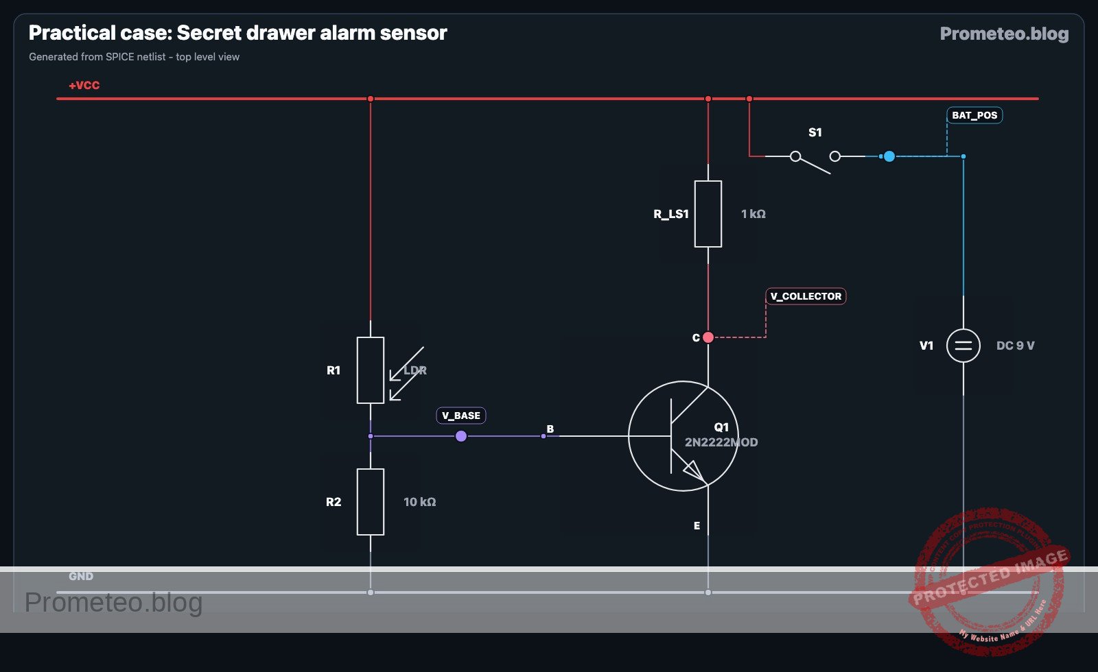
- VCC: Connect the positive terminal of V1 and one side of SW1. Connect the other side of SW1 to the main
VCCrail. - 0 (GND): Connect the negative terminal of V1, the Emitter of Q1, and one leg of R2.
- V_BASE: Connect the other leg of R2, one leg of R1, and the Base of Q1.
- VCC (Connection): Connect the other leg of R1 to the
VCCrail. - V_COLLECTOR: Connect the Collector of Q1 to the negative wire of LS1.
- VCC (Load): Connect the positive wire of LS1 to the
VCCrail.
Conceptual block diagram
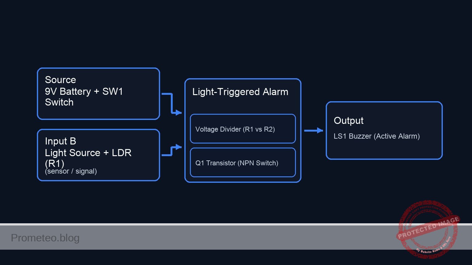
Schematic
[ INPUTS / POWER ]                  [ LOGIC / CONTROL ]                     [ OUTPUT ]

                                             (VCC Rail)
    [ 9 V Battery ] --> [ SW1 Switch ] --+------->+----------------------------------+
                                        |        |                                  |
                                        |        v                                  v
    [ Light Source ] --> [ LDR (R1) ] --+--> [ Voltage Divider ]                    |
                         (Sensor)            [ (Node: V_BASE)  ] --(Trigger)--> [ Q1 Transistor ]
                                        +--> [ R1 vs R2 Logic  ]                [ (NPN Switch)  ] --(Ground Path)--> [ LS1 Buzzer ]
                                        |                                       [ Collector Pin ]                    (Active Alarm)
    [ Resistor R2 ] ----(Pull-Down)-----+                                           |
    (10k Ohm)                                                                       v
                                                                                 [ GND ]
Electrical diagram
Measurements and tests
Follow these steps to validate the circuit operation:
- LDR Resistance Check:
- Set your multimeter to measure Resistance (Ω).
- Measure R1 in full light; it should read a low value (e.g., 500 Ω – 2 kΩ).
- Cover R1 completely; it should read a high value (e.g., > 100 kΩ).
- Voltage Divider Test:
- Power on the circuit (
VCC= 9 V). - Set multimeter to DC Voltage. Connect the black probe to 0 (GND) and the red probe to V_BASE.
- In Dark: The voltage should be close to 0 V (below 0.6 V).
- In Light: The voltage should rise significantly (above 0.7 V).
- Power on the circuit (
- Output Verification:
- Expose the sensor to light. The buzzer LS1 should sound.
- Cover the sensor with your hand. The buzzer should stop immediately.
SPICE netlist and simulation
Reference SPICE Netlist (ngspice) — excerptFull SPICE netlist (ngspice)
* Practical case: Secret drawer alarm sensor
* Ngspice Netlist
*
* Circuit Description:
* A light-activated alarm using a photoresistor (LDR) and an NPN transistor.
* When the drawer opens (Light), LDR resistance drops, Base voltage rises,
* Q1 turns ON, and the Buzzer sounds.
*
* Simulation Scenario:
* 0ms - 2ms: System OFF (Master Switch Open).
* 2ms: Master Switch closes (System Armed). Drawer is Closed (Dark).
* 5ms: Drawer Opens (Light hits LDR). Alarm triggers.

* --- Power Supply (V1) ---
* 9V DC Battery
V1 BAT_POS 0 DC 9

* --- Master Switch (SW1) ---
* Connects Battery Positive to Main VCC Rail.
* Modeled as a voltage-controlled switch closing at t=2ms.
* ... (truncated in public view) ...
Copy this content into a .cir file and run with ngspice.
* Practical case: Secret drawer alarm sensor
* Ngspice Netlist
*
* Circuit Description:
* A light-activated alarm using a photoresistor (LDR) and an NPN transistor.
* When the drawer opens (Light), LDR resistance drops, Base voltage rises,
* Q1 turns ON, and the Buzzer sounds.
*
* Simulation Scenario:
* 0ms - 2ms: System OFF (Master Switch Open).
* 2ms: Master Switch closes (System Armed). Drawer is Closed (Dark).
* 5ms: Drawer Opens (Light hits LDR). Alarm triggers.

* --- Power Supply (V1) ---
* 9V DC Battery
V1 BAT_POS 0 DC 9

* --- Master Switch (SW1) ---
* Connects Battery Positive to Main VCC Rail.
* Modeled as a voltage-controlled switch closing at t=2ms.
S1 BAT_POS VCC CTRL_SW 0 SW_MODEL
V_SW_CTRL CTRL_SW 0 PULSE(0 5 2ms 1u 1u 100ms)
.model SW_MODEL SW(Vt=2.5 Ron=0.01 Roff=100Meg)

* --- Photoresistor (R1 / LDR) ---
* LDR GL5528 connecting VCC to Base.
* Modeled as a behavioral resistor B_R1.
* Resistance logic controlled by V_LDR_RES:
*   Dark (Closed) = 1 MegOhm
*   Light (Open)  = 2 kOhm
* Simulation: Transitions from Dark to Light at t=5ms.
V_LDR_RES RES_CTRL 0 PWL(0 1Meg 4.99ms 1Meg 5ms 2k)
B_R1 VCC V_BASE I=(V(VCC) - V(V_BASE)) / V(RES_CTRL)

* --- Resistor (R2) ---
* 10k Ohm pull-down resistor from Base to Ground.
R2 V_BASE 0 10k

* --- Transistor (Q1) ---
* 2N2222 NPN Transistor acting as the switch for the buzzer.
* Connections: Collector=V_COLLECTOR, Base=V_BASE, Emitter=0
Q1 V_COLLECTOR V_BASE 0 2N2222MOD

* --- Buzzer (LS1) ---
* 9V Active Piezo Buzzer.
* Modeled as a 1k Ohm resistive load connected between VCC and Collector.
* (Not modeled as a voltage source per requirements).
R_LS1 VCC V_COLLECTOR 1k

* --- Component Models ---
.model 2N2222MOD NPN(Is=14.34f Xti=3 Eg=1.11 Vaf=74.03 Bf=255.9 Ne=1.307 Ise=14.34f Ikf=.2847 Xtb=1.5 Br=6.092 Nc=2 Isc=0 Ikr=0 Rc=1 Cjc=7.306p Mjc=.3416 Vjc=.75 Fc=.5 Cje=22.01p Mje=.377 Vje=.75 Tr=46.91n Tf=411.1p Itf=.6 Vtf=1.7 Xtf=3 Rb=10)

* --- Analysis Directives ---
.op
* Transient analysis for 10ms to capture the sequence.
.tran 10u 10ms

* Print directives to verify operation
* V(VCC): Power rail status
* V(V_BASE): Transistor drive voltage (Low=Dark, High=Light)
* V(V_COLLECTOR): Output node (High=Off, Low=Alarm On)
.print tran V(VCC) V(V_BASE) V(V_COLLECTOR)

.end
Simulation Results (Transient Analysis)

Show raw data table (1057 rows)
Index   time            v(vcc)          v(v_base)       v(v_collector)
0	0.000000e+00	8.999090e-02	8.909999e-04	8.999089e-02
1	1.000000e-07	8.999090e-02	8.909999e-04	8.999089e-02
2	2.000000e-07	8.999090e-02	8.909999e-04	8.999089e-02
3	4.000000e-07	8.999090e-02	8.909999e-04	8.999089e-02
4	8.000000e-07	8.999090e-02	8.909999e-04	8.999089e-02
5	1.600000e-06	8.999090e-02	8.909999e-04	8.999089e-02
6	3.200000e-06	8.999090e-02	8.909999e-04	8.999089e-02
7	6.400000e-06	8.999090e-02	8.909999e-04	8.999089e-02
8	1.280000e-05	8.999090e-02	8.909999e-04	8.999089e-02
9	2.280000e-05	8.999090e-02	8.909999e-04	8.999089e-02
10	3.280000e-05	8.999090e-02	8.909999e-04	8.999089e-02
11	4.280000e-05	8.999090e-02	8.909999e-04	8.999089e-02
12	5.280000e-05	8.999090e-02	8.909999e-04	8.999089e-02
13	6.280000e-05	8.999090e-02	8.909999e-04	8.999089e-02
14	7.280000e-05	8.999090e-02	8.909999e-04	8.999089e-02
15	8.280000e-05	8.999090e-02	8.909999e-04	8.999089e-02
16	9.280000e-05	8.999090e-02	8.909999e-04	8.999089e-02
17	1.028000e-04	8.999090e-02	8.909999e-04	8.999089e-02
18	1.128000e-04	8.999090e-02	8.909999e-04	8.999089e-02
19	1.228000e-04	8.999090e-02	8.909999e-04	8.999089e-02
20	1.328000e-04	8.999090e-02	8.909999e-04	8.999089e-02
21	1.428000e-04	8.999090e-02	8.909999e-04	8.999089e-02
22	1.528000e-04	8.999090e-02	8.909999e-04	8.999089e-02
23	1.628000e-04	8.999090e-02	8.909999e-04	8.999089e-02
... (1033 more rows) ...
Common mistakes and how to avoid them
- Reversing the Voltage Divider: If you swap R1 (LDR) and R2 (Fixed Resistor), the alarm will sound in the dark and stop in the light (Inverse logic). Ensure R1 is connected to
VCCand R2 toGND. - Using a Passive Buzzer: A passive buzzer requires an oscillating AC signal to make sound. This circuit provides DC. You must use an Active Buzzer (which has an internal oscillator).
- Transistor Pinout Errors: Confusing the Collector (C) and Emitter (E) is common. For the 2N2222 in a TO-92 package, verify the pinout datasheet; usually, with the flat side facing you, the pins are E-B-C or E-B-C depending on the manufacturer.
Troubleshooting
- Buzzer sounds continuously (even in dark):
- Ambient light is too strong. Place the circuit in a box.
- R2 value is too high. Try replacing R2 with a lower value (e.g., 4.7 kΩ) to pull the base voltage down harder.
- Buzzer never sounds:
- R2 value is too low.
- LS1 is connected backwards (check polarity).
- Q1 is damaged or connected incorrectly.
- Buzzer is too quiet:
- Battery voltage might be low.
- Ensure the buzzer is rated for the supply voltage used (9 V).
Possible improvements and extensions
- Sensitivity Control: Replace the fixed resistor R2 with a 50 kΩ potentiometer. This allows you to fine-tune exactly how much light is needed to trigger the alarm.
- Latching Alarm: Add a Silicon Controlled Rectifier (SCR) instead of the NPN transistor, or add a feedback loop. This would keep the alarm sounding even if the thief quickly closes the drawer again, forcing a manual reset.
More Practical Cases on Prometeo.blog
Find this product and/or books on this topic on Amazon
As an Amazon Associate, I earn from qualifying purchases. If you buy through this link, you help keep this project running.
Quick Quiz

Telecommunications Electronics Engineer and Computer Engineer (official degrees in Spain).