Practical case: Noise suppression with RF choke

Level: Medium – Demonstrate the high impedance of the inductor at high frequencies to block noise in power lines.

Objective and use case

You will construct an LR low-pass filter using an RF choke to isolate a DC power line from high-frequency AC noise. By superimposing an AC signal onto a DC voltage supply, you will observe how the inductor’s frequency-dependent reactance permits DC to pass while heavily attenuating high-frequency noise before it reaches the load.

This circuit concept is highly useful in the real world for:
* Preventing high-frequency switching noise from entering sensitive analog sensor circuits.
* Filtering out radio frequency interference (RFI) from long power supply lines.
* Isolating different functional blocks that share a common power rail on a PCB.
* Protecting automotive audio and communication electronics from alternator whine.

Expected outcome:
* The mixed input signal (V_IN_MIX) will display a steady DC offset combined with significant high-frequency ripples.
* The output voltage (V_OUT_CLEAN) across the load will show a stable DC level with the AC noise vastly reduced.
* An FFT (Fast Fourier Transform) analysis of the input will reveal a large 0 Hz (DC) component and a prominent high-frequency peak.
* An FFT analysis of the output will show the high-frequency peak almost completely suppressed, confirming the choke’s blocking action.

Target audience: Intermediate electronics students learning about reactive components and AC/DC superimposition.

Materials

  • V1: 5 V DC source, function: main DC power supply
  • V2: 500 mV peak sine wave AC source at 100 kHz, function: high-frequency noise simulator
  • L1: 1 mH inductor, function: RF choke to block high-frequency noise
  • R1: 100 Ω resistor, function: load simulation

Wiring guide

  • V1: connects between V_DC and 0
  • V2: connects between V_IN_MIX and V_DC
  • L1: connects between V_IN_MIX and V_OUT_CLEAN
  • R1: connects between V_OUT_CLEAN and 0

Conceptual block diagram

Conceptual block diagram — 1mH RF Choke
Quick read: inputs → main block → output (actuator or measurement). This summarizes the ASCII schematic below.

Schematic

[ V1: 5 V DC Source ] --(V_DC)--> [ V2: AC Noise Simulator ] --(V_IN_MIX)--> [ L1: 1mH RF Choke ] --(V_OUT_CLEAN)--> [ R1: 100 Ω Load ] --> GND
Electrical Schematic

Electrical diagram

Electrical diagram for case: Practical case: Noise suppression with RF choke
Generated from the validated SPICE netlist for this case.

🔒 This electrical diagram is premium. With the 7-day pass or the monthly membership you can unlock the complete didactic material and the print-ready PDF pack.🔓 See premium access plans

Measurements and tests

  1. Connect an oscilloscope probe to V_IN_MIX with the ground clip attached to node 0. Set the channel coupling to DC. You should observe a 5 V DC baseline with a 1 V peak-to-peak 100 kHz sine wave riding on top of it.
  2. Connect a second oscilloscope probe to V_OUT_CLEAN. Observe that the DC voltage remains at approximately 5 V, but the high-frequency 100 kHz ripple is drastically attenuated due to the high inductive reactance (XL = 2\pi fL) of the choke.
  3. Activate the FFT (Fast Fourier Transform) math function on the oscilloscope for the V_IN_MIX channel. Note the massive spike at 0 Hz (representing the 5 V DC component) and the distinct noise spike at 100 kHz.
  4. Apply the FFT function to the V_OUT_CLEAN channel. Compare the magnitude of the 100 kHz spike against the input measurement; it should be significantly reduced, successfully proving the inductor’s high-frequency blocking capabilities.

SPICE netlist and simulation

Reference SPICE Netlist (ngspice) — excerptFull SPICE netlist (ngspice)

* Noise suppression with RF choke
.width out=256

* Main DC power supply (5V)
V1 V_DC 0 DC 5

* High-frequency noise simulator (500mV peak, 100kHz sine wave superimposed on DC)
V2 V_IN_MIX V_DC SINE(0 500m 100k)

* RF choke to block high-frequency noise (1mH)
L1 V_IN_MIX V_OUT_CLEAN 1m

* Load simulation (100 ohms)
* ... (truncated in public view) ...

Copy this content into a .cir file and run with ngspice.

🔒 Part of this section is premium. With the 7-day pass or the monthly membership you can access the full content (materials, wiring, detailed build, validation, troubleshooting, variants and checklist) and download the complete print-ready PDF pack.

* Noise suppression with RF choke
.width out=256

* Main DC power supply (5V)
V1 V_DC 0 DC 5

* High-frequency noise simulator (500mV peak, 100kHz sine wave superimposed on DC)
V2 V_IN_MIX V_DC SINE(0 500m 100k)

* RF choke to block high-frequency noise (1mH)
L1 V_IN_MIX V_OUT_CLEAN 1m

* Load simulation (100 ohms)
R1 V_OUT_CLEAN 0 100

* Analysis directives
.op
* Simulate for 100us to capture 10 full cycles of the 100kHz noise
.tran 0.1u 100u
.print tran V(V_IN_MIX) V(V_OUT_CLEAN) V(V_DC) I(L1)

.end

Simulation Results (Transient Analysis)

Simulation Results (Transient Analysis)
Analysis: The simulation shows a 5V DC signal with a superimposed 500mV peak 100kHz sine wave at the input (V_IN_MIX ranges from 4.5V to 5.5V). At the output (V_OUT_CLEAN), the voltage ranges from 4.92V to 5.12V, indicating that the 1mH RF choke significantly attenuates the high-frequency noise while passing the DC component to the 100-ohm load.
Show raw data table (1008 rows)
Index   time            v(v_in_mix)     v(v_out_clean)  v(v_dc)         l1#branch
0	0.000000e+00	5.000000e+00	5.000000e+00	5.000000e+00	5.000000e-02
1	1.000000e-09	5.000314e+00	5.000000e+00	5.000000e+00	5.000000e-02
2	2.000000e-09	5.000628e+00	5.000000e+00	5.000000e+00	5.000000e-02
3	4.000000e-09	5.001257e+00	5.000000e+00	5.000000e+00	5.000000e-02
4	8.000000e-09	5.002513e+00	5.000001e+00	5.000000e+00	5.000001e-02
5	1.600000e-08	5.005026e+00	5.000004e+00	5.000000e+00	5.000004e-02
6	3.200000e-08	5.010052e+00	5.000016e+00	5.000000e+00	5.000016e-02
7	6.400000e-08	5.020101e+00	5.000064e+00	5.000000e+00	5.000064e-02
8	1.280000e-07	5.040169e+00	5.000256e+00	5.000000e+00	5.000256e-02
9	2.280000e-07	5.071384e+00	5.000808e+00	5.000000e+00	5.000808e-02
10	3.280000e-07	5.102316e+00	5.001665e+00	5.000000e+00	5.001665e-02
11	4.280000e-07	5.132845e+00	5.002818e+00	5.000000e+00	5.002818e-02
12	5.280000e-07	5.162850e+00	5.004261e+00	5.000000e+00	5.004261e-02
13	6.280000e-07	5.192212e+00	5.005985e+00	5.000000e+00	5.005985e-02
14	7.280000e-07	5.220816e+00	5.007980e+00	5.000000e+00	5.007980e-02
15	8.280000e-07	5.248548e+00	5.010236e+00	5.000000e+00	5.010236e-02
16	9.280000e-07	5.275299e+00	5.012741e+00	5.000000e+00	5.012741e-02
17	1.028000e-06	5.300963e+00	5.015481e+00	5.000000e+00	5.015481e-02
18	1.128000e-06	5.325440e+00	5.018443e+00	5.000000e+00	5.018443e-02
19	1.228000e-06	5.348633e+00	5.021613e+00	5.000000e+00	5.021613e-02
20	1.328000e-06	5.370449e+00	5.024976e+00	5.000000e+00	5.024976e-02
21	1.428000e-06	5.390804e+00	5.028515e+00	5.000000e+00	5.028515e-02
22	1.528000e-06	5.409616e+00	5.032213e+00	5.000000e+00	5.032213e-02
23	1.628000e-06	5.426812e+00	5.036054e+00	5.000000e+00	5.036054e-02
... (984 more rows) ...

Common mistakes and how to avoid them

  • Using an inductor with a low self-resonant frequency (SRF): All inductors have parasitic winding capacitance. If the noise frequency exceeds the inductor’s SRF, the component behaves like a capacitor and allows high-frequency noise to pass straight through. Always verify the SRF is well above your target noise frequency.
  • Neglecting the inductor’s DC resistance (DCR): Inductors are made of coiled wire which naturally possesses resistance. High load currents passing through an inductor with high DCR will cause an unacceptable DC voltage drop. Choose a choke with an appropriately low DCR for your load.
  • Core saturation due to high DC current: If the load draws more continuous current than the inductor’s saturation rating (Isat), the core’s magnetic flux saturates. This causes the inductance to drop sharply, destroying its filtering capability. Always check the saturation current rating.

Troubleshooting

  • Symptom: High-frequency noise is still heavily present at V_OUT_CLEAN.
  • Cause: The inductor value is too low to provide significant reactance at the simulated noise frequency, or its SRF has been exceeded.
  • Fix: Increase the inductance value (e.g., scale from 10 µH to 1 mH) or verify the frequency limits of the specific choke being used.
  • Symptom: Significant DC voltage drop at V_OUT_CLEAN under load (e.g., reading 4 V instead of 5 V).
  • Cause: The inductor’s internal DC resistance (DCR) is too high relative to the load resistor R1.
  • Fix: Replace the inductor with a physically larger one that uses thicker wire, which lowers the DCR, or increase the load resistance if it’s drawing more current than intended.
  • Symptom: The choke gets excessively hot during operation.
  • Cause: The DC current drawn by the load exceeds the continuous thermal current rating (Irms) of the inductor.
  • Fix: Select a higher-rated power inductor capable of safely handling the steady-state load current.

Possible improvements and extensions

  • Form an LC Low-Pass Filter: Add a decoupling capacitor (e.g., 100 nF or 1 µF) parallel to the load (between V_OUT_CLEAN and 0). This creates a second-order filter, providing a much steeper roll-off and vastly superior noise attenuation compared to the simple LR configuration.
  • Implement a Pi-Filter: Use a Capacitor-Inductor-Capacitor (C-L-C) arrangement to provide bidirectional noise suppression. This not only cleans the power entering the load but also prevents any switching noise generated by the load from polluting the main DC supply line.

More Practical Cases on Prometeo.blog

Find this product and/or books on this topic on Amazon

Go to Amazon

As an Amazon Associate, I earn from qualifying purchases. If you buy through this link, you help keep this project running.

Quick Quiz

Question 1: What is the primary purpose of the inductor in the described circuit?


Question 2: What type of filter is constructed in this experiment?


Question 3: How does the inductor react to the DC portion of the signal?


Question 4: Which of the following is a real-world application of this circuit concept mentioned in the text?


Question 5: What will the mixed input signal (V_IN_MIX) display according to the expected outcomes?


Question 6: Based on the expected outcomes, what is the effect of the circuit on the output voltage (V_OUT_CLEAN)?


Question 7: What is the stated difficulty level of demonstrating the high impedance of the inductor in this context?


Question 8: What specific type of interference can this circuit filter out from long power supply lines?


Question 9: How does the circuit help different functional blocks that share a common power rail on a PCB?


Question 10: What component is specifically used as an RF choke in this low-pass filter circuit?


Carlos Núñez Zorrilla
Electronics & Computer Engineer

Telecommunications Electronics Engineer and Computer Engineer (official degrees in Spain).

Follow me:


Practical case: Resonance in LC tank circuit

Level: Medium | Analyze the energy exchange and determine the resonant frequency of an AC-driven LC tank.

Objective and use case

In this practical case, you will build a parallel LC tank circuit driven by an AC sine wave source through a series resistor. By sweeping the input frequency, you will observe the precise point where inductive and capacitive reactances cancel out, maximizing the circuit’s impedance.

Understanding LC resonance is essential in modern electronics because these circuits are the fundamental building blocks of frequency selection. Real-world applications include:
* Radio frequency (RF) tuning: Selecting a specific station’s frequency while rejecting others.
* Audio and signal filtering: Creating band-pass or band-stop (notch) filters to eliminate noise.
* Wireless power transfer: Maximizing the efficiency of inductive coupling between transmitter and receiver coils.
* Oscillator circuits: Generating stable clock signals for microcontrollers and transceivers.

Expected outcome:
* You will calculate the theoretical resonant frequency based on the chosen $L$ and $C$ values.
* The total current drawn from the source (Itotal) will drop to its minimum value at resonance.
* The voltage across the LC tank (VLC) will peak at the resonant frequency.
* You will observe how energy continuously sloshes back and forth between the capacitor’s electric field and the inductor’s magnetic field.

Target audience: Intermediate electronics students transitioning from DC basics to AC reactive circuits.

Materials

  • V1: 5 V peak-to-peak AC voltage source, function: sine wave generator for frequency sweep
  • R1: 1 kΩ resistor, function: source impedance to allow voltage variations across the tank
  • L1: 10 mH inductor, function: magnetic energy storage
  • C1: 100 nF ceramic or film capacitor, function: electric energy storage

Wiring guide

  • V1: Connect the positive terminal to node IN and the negative terminal to node 0 (GND).
  • R1: Connect one pin to node IN and the other pin to node TANK.
  • L1: Connect one pin to node TANK and the other pin to node 0 (GND).
  • C1: Connect one pin to node TANK and the other pin to node 0 (GND).

Conceptual block diagram

Conceptual block diagram — LC Tank Circuit
Quick read: inputs → main block → output (actuator or measurement). This summarizes the ASCII schematic below.

Schematic

[ V1: 5 V AC ] --(IN)--> [ R1: 1k ohm ] --(Node TANK)--+--> [ L1: 10mH ] --> GND
                                                      |
                                                      +--> [ C1: 100nF ] --> GND
Electrical Schematic

Electrical diagram

Electrical diagram for case: Practical case: Resonance in LC tank circuit
Generated from the validated SPICE netlist for this case.

🔒 This electrical diagram is premium. With the 7-day pass or the monthly membership you can unlock the complete didactic material and the print-ready PDF pack.🔓 See premium access plans

Measurements and tests

  1. Calculate the theoretical resonant frequency (fr):
    Use the formula fr = (1 / 2\pi\sqrtLC). With L = 10 mH and C = 100 nF, the expected resonant frequency is approximately 5032 Hz.
  2. Set up the frequency sweep:
    Configure V1 to output a 5 V peak-to-peak sine wave. Begin with a frequency of 1 kHz and gradually increase it up to 10 kHz.
  3. Measure VLC (Tank Voltage):
    Monitor the voltage amplitude at node TANK relative to node 0 (GND) using an oscilloscope or an AC voltmeter. As you approach 5 kHz, the voltage amplitude will rise steadily, hitting a sharp maximum exactly at resonance, and then fall as the frequency increases further.
  4. Measure Itotal (Source Current):
    Measure the current flowing through R1 (this can be done by observing the voltage difference between IN and TANK and applying Ohm’s law: Itotal = ((VIN – VTANK) / R1)). Note that at resonance, the parallel LC tank exhibits maximum impedance, meaning Itotal will drop to its minimum.
  5. Calculate the circuit’s Q-factor:
    Identify the -3dB (half-power) frequencies above and below the resonance peak to find the bandwidth ($BW$). The Quality Factor is Q = (fr / BW).

SPICE netlist and simulation

Reference SPICE Netlist (ngspice) — excerptFull SPICE netlist (ngspice)

* Practical case: Resonance in LC tank circuit
.width out=256

* 5V peak-to-peak implies an amplitude of 2.5V. 
* The resonant frequency of 10mH and 100nF is approximately 5033 Hz.
* We configure V1 with both a transient sine wave at resonance and an AC magnitude for optional AC analysis.
V1 IN 0 DC 0 AC 2.5 SIN(0 2.5 5033)

* Source impedance
R1 IN TANK 1k

* LC Tank circuit components
L1 TANK 0 10mH
* ... (truncated in public view) ...

Copy this content into a .cir file and run with ngspice.

🔒 Part of this section is premium. With the 7-day pass or the monthly membership you can access the full content (materials, wiring, detailed build, validation, troubleshooting, variants and checklist) and download the complete print-ready PDF pack.

* Practical case: Resonance in LC tank circuit
.width out=256

* 5V peak-to-peak implies an amplitude of 2.5V. 
* The resonant frequency of 10mH and 100nF is approximately 5033 Hz.
* We configure V1 with both a transient sine wave at resonance and an AC magnitude for optional AC analysis.
V1 IN 0 DC 0 AC 2.5 SIN(0 2.5 5033)

* Source impedance
R1 IN TANK 1k

* LC Tank circuit components
L1 TANK 0 10mH
C1 TANK 0 100nF

* Operating point and Transient analysis
.op
.tran 1u 2m

* Print directives for logging the input and output (resonance) nodes
.print tran V(IN) V(TANK) I(L1)

.end

Simulation Results (Transient Analysis)

Simulation Results (Transient Analysis)
Analysis: The transient simulation shows the input voltage V(IN) oscillating as a sine wave with a 2.5V amplitude (5V peak-to-peak). The voltage at the tank node V(TANK) closely follows V(IN) with nearly the same amplitude, and the inductor current oscillates, confirming the resonant behavior of the LC tank circuit at the specified frequency.
Show raw data table (2015 rows)
Index   time            v(in)           v(tank)         l1#branch
0	0.000000e+00	0.000000e+00	0.000000e+00	0.000000e+00
1	1.000000e-08	7.905818e-04	7.905026e-08	7.905026e-14
2	1.084006e-08	8.569951e-04	8.624878e-08	8.629565e-14
3	1.252017e-08	9.898217e-04	1.017615e-07	1.020896e-13
4	1.588039e-08	1.255475e-03	1.394809e-07	1.426210e-13
5	2.260084e-08	1.786781e-03	2.416948e-07	2.707046e-13
6	3.604174e-08	2.849394e-03	5.532131e-07	8.049184e-13
7	5.708432e-08	4.512980e-03	1.327631e-06	2.783809e-12
8	8.603868e-08	6.802053e-03	2.965106e-06	8.998482e-12
9	1.305078e-07	1.031768e-02	6.769425e-06	3.064276e-11
10	1.955195e-07	1.545732e-02	1.514065e-05	1.018634e-10
11	2.946313e-07	2.329267e-02	3.431881e-05	3.469641e-10
12	4.417944e-07	3.492633e-02	7.707420e-05	1.166612e-09
13	6.644501e-07	5.252635e-02	1.741480e-04	3.963414e-09
14	9.972436e-07	7.882720e-02	3.917455e-04	1.337970e-08
15	1.499113e-06	1.184727e-01	8.834917e-04	4.537981e-08
16	2.252017e-06	1.778899e-01	1.987598e-03	1.534626e-07
17	3.252017e-06	2.566456e-01	4.126641e-03	4.591745e-07
18	4.252017e-06	3.351447e-01	7.022468e-03	1.016630e-06
19	5.252017e-06	4.133086e-01	1.066173e-02	1.900840e-06
20	6.252017e-06	4.910592e-01	1.502968e-02	3.185410e-06
21	7.252017e-06	5.683189e-01	2.011023e-02	4.942405e-06
22	8.252017e-06	6.450102e-01	2.588597e-02	7.242215e-06
23	9.252017e-06	7.210565e-01	3.233820e-02	1.015342e-05
... (1991 more rows) ...

Common mistakes and how to avoid them

  • Using a polarized capacitor in an AC circuit: Electrolytic capacitors are generally polarized and can fail or explode if subjected to reversing AC voltages. Always use non-polarized capacitors (like ceramic or film) for an LC tank.
  • Ignoring the inductor’s Equivalent Series Resistance (ESR): Real inductors consist of long coils of wire, adding parasitic DC resistance to the tank. If the measured Q-factor is much lower than expected (resulting in a wider, flatter peak), inductor ESR is usually the culprit.
  • Confusing angular frequency (\omega) with standard frequency ($f$): Remember that \omega = (1 / \sqrtLC) yields results in radians per second. You must divide by 2\pi to get the frequency in Hertz.

Troubleshooting

  • Symptom: The measured resonant frequency is significantly higher or lower than the calculated 5032 Hz.
    • Cause: Component tolerances. Standard ceramic capacitors can have a ±20% tolerance, and inductors often have ±10%.
    • Fix: Measure the exact values of L1 and C1 using an LCR meter and recalculate the expected frequency.
  • Symptom: VLC shows no noticeable peak during the sweep; the voltage remains relatively flat.
    • Cause: The chosen frequency sweep range does not cover the resonant point, or R1 is too small, effectively shorting the tank to the rigid voltage source.
    • Fix: Double-check the math for your specific $L$ and $C$ values to ensure the sweep range encompasses fr. Ensure R1 is adequately sized (1 kΩ is a good starting point).
  • Symptom: Signal distortion or clipping is observed at node TANK.
    • Cause: The AC source might be overdriving the circuit, or core saturation is occurring in the inductor (if using a very small ferrite core at high currents).
    • Fix: Reduce the amplitude of V1 from 5 V to 1 V peak-to-peak and check if the sine wave becomes clean again.

Possible improvements and extensions

  • Vary the damping resistor: Swap R1 for different values (e.g., 470 Ω, 10 kΩ) or add a resistor directly in parallel with the LC tank. Observe and chart how this affects the sharpness of the resonance peak (the Q-factor).
  • Build an active oscillator: Remove the AC source and connect the LC tank to a transistor or an op-amp with positive feedback (such as a Colpitts or Hartley configuration) to create a standalone circuit that generates its own continuous sine wave at the resonant frequency.

More Practical Cases on Prometeo.blog

Find this product and/or books on this topic on Amazon

Go to Amazon

As an Amazon Associate, I earn from qualifying purchases. If you buy through this link, you help keep this project running.

Quick Quiz

Question 1: What is the primary objective of sweeping the input frequency in the described LC tank circuit?


Question 2: In a parallel LC tank circuit at resonance, what happens to the total current drawn from the source?


Question 3: What happens to the voltage across the LC tank at the resonant frequency?


Question 4: How does energy behave in an LC tank circuit at resonance?


Question 5: Which of the following is a real-world application of LC resonance mentioned in the text?


Question 6: What is the function of the series resistor (R1) in this practical case?


Question 7: What type of source is used to drive the LC tank circuit in this practical case?


Question 8: In the context of audio and signal filtering, what can LC circuits be used to create?


Question 9: Why is understanding LC resonance essential for wireless power transfer?


Question 10: Who is the target audience for this practical case?


Carlos Núñez Zorrilla
Electronics & Computer Engineer

Telecommunications Electronics Engineer and Computer Engineer (official degrees in Spain).

Follow me:


Practical case: Boost converter storage

Level: Medium | Understand magnetic energy storage to boost voltage.

Objective and use case

In this practical case, you will build a basic open-loop Boost converter to demonstrate how an inductor stores and releases magnetic energy to step up a DC voltage.

Why it is useful:
* Allows battery-powered devices to operate at higher voltages (e.g., generating 5 V from a single 3.7 V Li-ion cell).
* Drives strings of LEDs that require a constant, high forward voltage.
* Captures and steps up voltage in energy harvesting and regenerative braking systems.
* Provides versatile power rails in compact portable electronics without requiring multiple batteries.

Expected outcome:
* You will observe the inductor current (I_inductor) ramping up when the switch is closed and ramping down when it opens.
* The output voltage (V_out) will be demonstrably higher than the input voltage source.
* You will record the direct relationship between the switch’s Duty Cycle and the resulting V_out magnitude.

Target audience and level:
Intermediate electronics students learning the fundamentals of switch-mode power supplies.

Materials

  • V1: 5 V DC source, function: main power input
  • V2: Pulse voltage source (0-5 V, 100kHz, 50% duty cycle), function: PWM signal for the switch
  • L1: 100 µH inductor, function: magnetic energy storage
  • M1: N-channel MOSFET (e.g., IRLZ44N), function: main switching element
  • D1: Schottky diode (e.g., 1N5819), function: prevents reverse current from capacitor
  • C1: 47 µF capacitor, function: output voltage smoothing
  • R1: 100 Ω resistor, function: basic load to discharge capacitor

Wiring guide

  • V1: connects between VIN and 0 (GND).
  • V2: connects between GATE_PWM and 0 (GND).
  • L1: connects between VIN and SW_NODE.
  • M1: Drain connects to SW_NODE, Gate connects to GATE_PWM, Source connects to 0 (GND).
  • D1: Anode connects to SW_NODE, Cathode connects to VOUT.
  • C1: connects between VOUT and 0 (GND).
  • R1: connects between VOUT and 0 (GND).

Conceptual block diagram

Conceptual block diagram — Boost Converter
Quick read: inputs → main block → output (actuator or measurement). This summarizes the ASCII schematic below.

Schematic

Control Signal:
[ V2: PWM (0-5 V) ] --(GATE_PWM)--> [ M1:Gate ]

Power & Switching Path:
[ V1: 5 V DC ] --(VIN)--> [ L1: 100µH ] --(SW_NODE)--> [ M1:Drain ] --(Switch)--> [ M1:Source ] --> GND
                                             |
Boost Output & Load:                         |
                                             +--> [ D1: Schottky ] --(VOUT)--> [ R1: 100 Ω ] --> GND
                                                                       |
                                                                       +--> [ C1: 47µF ] --> GND
Electrical Schematic

Electrical diagram

Electrical diagram for case: Practical case: Boost converter storage
Generated from the validated SPICE netlist for this case.

🔒 This electrical diagram is premium. With the 7-day pass or the monthly membership you can unlock the complete didactic material and the print-ready PDF pack.🔓 See premium access plans

Measurements and tests

  1. Initial state check: Apply V1 (5 V) with V2 turned off (0% duty cycle). Measure VOUT. The voltage should be roughly 4.7 V (the 5 V input minus the forward voltage drop of the Schottky diode).
  2. Switching activation: Activate V2 to supply a 100kHz square wave at a 50% duty cycle. Measure VOUT across R1. The voltage should rise to approximately 9 V-10 V, demonstrating the step-up action.
  3. Inductor current observation: Probe the current flowing through L1 (I_inductor). You will observe a triangular waveform. The upward slope occurs while M1 is ON (energy storage), and the downward slope occurs while M1 is OFF (energy release to VOUT).
  4. Duty Cycle mapping: Adjust the Duty Cycle of V2 from 30% to 70% in 10% increments. Record VOUT at each step to verify that a higher duty cycle yields a higher output voltage.

SPICE netlist and simulation

Reference SPICE Netlist (ngspice) — excerptFull SPICE netlist (ngspice)

* Boost converter storage

* Main power input
V1 VIN 0 DC 5

* PWM signal for the switch (100kHz, 50% duty cycle)
V2 GATE_PWM 0 PULSE(0 5 0 10n 10n 5u 10u)

* Magnetic energy storage
L1 VIN SW_NODE 100u

* Main switching element (N-channel MOSFET)
* Drain: SW_NODE, Gate: GATE_PWM, Source: 0, Bulk: 0
M1 SW_NODE GATE_PWM 0 0 IRLZ44N

* Prevents reverse current from capacitor
* Anode: SW_NODE, Cathode: VOUT
D1 SW_NODE VOUT 1N5819

* Output voltage smoothing
* ... (truncated in public view) ...

Copy this content into a .cir file and run with ngspice.

🔒 Part of this section is premium. With the 7-day pass or the monthly membership you can access the full content (materials, wiring, detailed build, validation, troubleshooting, variants and checklist) and download the complete print-ready PDF pack.

* Boost converter storage

* Main power input
V1 VIN 0 DC 5

* PWM signal for the switch (100kHz, 50% duty cycle)
V2 GATE_PWM 0 PULSE(0 5 0 10n 10n 5u 10u)

* Magnetic energy storage
L1 VIN SW_NODE 100u

* Main switching element (N-channel MOSFET)
* Drain: SW_NODE, Gate: GATE_PWM, Source: 0, Bulk: 0
M1 SW_NODE GATE_PWM 0 0 IRLZ44N

* Prevents reverse current from capacitor
* Anode: SW_NODE, Cathode: VOUT
D1 SW_NODE VOUT 1N5819

* Output voltage smoothing
C1 VOUT 0 47u

* Basic load to discharge capacitor
R1 VOUT 0 100

* Models
.model IRLZ44N NMOS(Level=1 VTO=2.0 KP=10.0 RS=0.05 RD=0.05)
.model 1N5819 D(IS=1e-6 RS=0.1 N=1.05 EG=0.69 XTI=2)

* Output Directives
* VOUT is the main output, GATE_PWM is the input stimulus
.print tran V(VOUT) V(GATE_PWM) V(SW_NODE) V(VIN) I(L1)

* Analysis
* Time constant is R*C = 4.7ms. Simulating for 10ms to observe steady-state boost voltage.
.op
.tran 0.1u 10m

.end

Simulation Results (Transient Analysis)

Simulation Results (Transient Analysis)
Analysis: The simulation shows the boost converter operating correctly. The output voltage (VOUT) starts near 5V and rises to a steady-state value of approximately 9.6V, with the switch node (SW_NODE) switching between ~0V and ~10V as driven by the 100kHz PWM signal.
Show raw data table (119800 rows)
Index   time            v(vout)         v(gate_pwm)     v(sw_node)      v(vin)          l1#branch
0	0.000000e+00	4.702912e+00	0.000000e+00	5.000000e+00	5.000000e+00	4.702912e-02
1	1.000000e-10	4.702912e+00	5.000000e-02	4.999798e+00	5.000000e+00	4.702912e-02
2	2.000000e-10	4.702912e+00	1.000000e-01	4.999798e+00	5.000000e+00	4.702912e-02
3	4.000000e-10	4.702912e+00	2.000000e-01	4.999797e+00	5.000000e+00	4.702912e-02
4	8.000000e-10	4.702912e+00	4.000000e-01	4.999797e+00	5.000000e+00	4.702912e-02
5	1.600000e-09	4.702912e+00	8.000000e-01	4.999797e+00	5.000000e+00	4.702912e-02
6	3.200000e-09	4.702912e+00	1.600000e+00	4.999797e+00	5.000000e+00	4.702913e-02
7	6.400000e-09	4.702910e+00	3.200000e+00	8.651034e-03	5.000000e+00	4.710899e-02
8	1.000000e-08	4.702907e+00	5.000000e+00	6.306948e-03	5.000000e+00	4.728872e-02
9	1.064000e-08	4.702906e+00	5.000000e+00	6.311218e-03	5.000000e+00	4.732068e-02
10	1.192000e-08	4.702905e+00	5.000000e+00	6.319746e-03	5.000000e+00	4.738460e-02
11	1.448000e-08	4.702902e+00	5.000000e+00	6.336800e-03	5.000000e+00	4.751244e-02
12	1.960000e-08	4.702897e+00	5.000000e+00	6.370908e-03	5.000000e+00	4.776811e-02
13	2.984000e-08	4.702887e+00	5.000000e+00	6.439123e-03	5.000000e+00	4.827946e-02
14	5.032000e-08	4.702866e+00	5.000000e+00	6.575553e-03	5.000000e+00	4.930212e-02
15	9.128000e-08	4.702825e+00	5.000000e+00	6.848406e-03	5.000000e+00	5.134738e-02
16	1.732000e-07	4.702743e+00	5.000000e+00	7.394086e-03	5.000000e+00	5.543754e-02
17	2.732000e-07	4.702643e+00	5.000000e+00	8.060152e-03	5.000000e+00	6.042981e-02
18	3.732000e-07	4.702543e+00	5.000000e+00	8.726166e-03	5.000000e+00	6.542142e-02
19	4.732000e-07	4.702443e+00	5.000000e+00	9.392128e-03	5.000000e+00	7.041236e-02
20	5.732000e-07	4.702343e+00	5.000000e+00	1.005804e-02	5.000000e+00	7.540264e-02
21	6.732000e-07	4.702243e+00	5.000000e+00	1.072390e-02	5.000000e+00	8.039225e-02
22	7.732000e-07	4.702143e+00	5.000000e+00	1.138970e-02	5.000000e+00	8.538119e-02
23	8.732000e-07	4.702043e+00	5.000000e+00	1.205546e-02	5.000000e+00	9.036947e-02
... (119776 more rows) ...

Common mistakes and how to avoid them

  • Using a standard rectifier diode (e.g., 1N4007): Standard diodes are too slow to turn off at 100kHz, leading to massive switching losses and poor voltage conversion. Always use a fast-recovery or Schottky diode like the 1N5819.
  • Inductor core saturation: If the inductor’s maximum current rating is lower than the peak switching current, the magnetic core will saturate. The inductor will then act as a short circuit, potentially destroying the MOSFET. Always verify the inductor’s saturation current rating.
  • Operating without a load: Running a boost converter with no load resistor (R1) can cause the output voltage to continuously rise with every switching cycle, theoretically reaching infinity and destroying the output capacitor or MOSFET. Always include a minimum load.

Troubleshooting

  • Symptom: Output voltage equals the input voltage (minus diode drop).
  • Cause: The MOSFET is not switching. V2 might be disconnected or the voltage level is too low to surpass the MOSFET’s gate threshold.
  • Fix: Check the GATE_PWM signal with an oscilloscope. Use a logic-level MOSFET if your PWM signal is limited to 3.3 V or 5 V.
  • Symptom: MOSFET becomes extremely hot very quickly.
  • Cause: The inductor is saturating, or the MOSFET has a high ON-resistance (RDS(on)) and is experiencing high conduction losses.
  • Fix: Swap the inductor for one with a higher current rating. Ensure the gate drive voltage is sufficient to turn the MOSFET completely ON.
  • Symptom: Unstable or highly rippled output voltage.
  • Cause: The output capacitor C1 is too small for the load or has a high Equivalent Series Resistance (ESR).
  • Fix: Increase the capacitance of C1 or place a ceramic capacitor in parallel with the electrolytic capacitor to lower the overall ESR.

Possible improvements and extensions

  • Closed-loop control: Add a voltage divider at the output connected to an error amplifier or microcontroller analog input. Dynamically adjust the PWM duty cycle to maintain a constant VOUT regardless of changes in R1 (the load).
  • Synchronous rectification: Replace the Schottky diode D1 with a second P-channel or driven N-channel MOSFET. Switching this second MOSFET synchronously (inversely to M1) reduces the voltage drop typical of a diode, significantly improving overall converter efficiency.

More Practical Cases on Prometeo.blog

Find this product and/or books on this topic on Amazon

Go to Amazon

As an Amazon Associate, I earn from qualifying purchases. If you buy through this link, you help keep this project running.

Quick Quiz

Question 1: What is the primary purpose of the Boost converter in this practical case?


Question 2: Which component is responsible for storing and releasing magnetic energy?


Question 3: What happens to the inductor current when the switch is closed?


Question 4: Which of the following is a mentioned use case for a Boost converter?


Question 5: What happens to the inductor current when the switch opens?


Question 6: What parameter of the switch has a direct relationship with the magnitude of the output voltage?


Question 7: How can a Boost converter benefit battery-powered devices?


Question 8: What role does the Boost converter play in energy harvesting systems?


Question 9: What is the expected relationship between the output voltage and the input voltage source?


Question 10: Who is the target audience for this practical case?


Carlos Núñez Zorrilla
Electronics & Computer Engineer

Telecommunications Electronics Engineer and Computer Engineer (official degrees in Spain).

Follow me:


Practical case: Inductive peak protection

Inductive peak protection prototype (Maker Style)

Level: Medium | Objective: Analyze the transient voltage generated when disconnecting an inductor and mitigate it using a flyback diode.

Objective and use case

In this practical case, you will build a switched inductor circuit monitored by an oscilloscope to observe the destructive voltage spike (inductive kickback) that occurs when current is abruptly interrupted. You will then install a flyback diode in parallel with the inductive load to safely clamp this transient voltage.

Why it is useful:
* Prevents catastrophic overvoltage damage to sensitive switching components such as transistors, MOSFETs, and microcontroller pins.
* Significantly reduces electromagnetic interference (EMI) and radio frequency interference (RFI) caused by high-voltage arcing across mechanical switch contacts.
* Increases the reliability, safety, and lifespan of power supply systems, motor controllers, and relay-driven circuits.

Expected outcome:
* Without the diode, opening the switch will produce a massive negative voltage spike on the oscilloscope, often reaching hundreds of volts.
* With the flyback diode installed, the transient spike will be immediately clamped to a safe level of approximately -0.7 V.
* The stored magnetic energy will safely dissipate as a steadily decaying circulating current through the inductor-resistor-diode loop.

Target audience and level: Intermediate electronics students learning about reactive components, energy storage, and circuit protection techniques.

Materials

  • V1: 12 V DC supply, function: main power source
  • SW1: SPST toggle or push-button switch, function: circuit connection control
  • L1: 100 mH inductor, function: magnetic energy storage
  • R1: 100 Ω resistor, function: limits steady-state current to 120 mA
  • D1: 1N4007 rectifier diode, function: flyback protection

Wiring guide

  • V1: connects between node VCC (positive) and node 0 (ground).
  • SW1: connects between node VCC and node SW_OUT.
  • L1: connects between node SW_OUT and node L_MID.
  • R1: connects between node L_MID and node 0.
  • D1: connects between node 0 (Anode) and node SW_OUT (Cathode) for reverse bias during normal closed-switch operation.

Conceptual block diagram

Conceptual block diagram — Flyback Protection
Quick read: inputs → main block → output (actuator or measurement). This summarizes the ASCII schematic below.

Schematic

VCC (12 V) --> [ SW1: SPST Switch ] --(SW_OUT)--> [ L1: 100mH Inductor ] --(L_MID)--> [ R1: 100 Ω Resistor ] --> GND
                                         ^
                                         |
                              (Cathode)  |
                           [ D1: 1N4007 Flyback ]
                              (Anode)    ^
                                         |
                                        GND
Electrical Schematic

Electrical diagram

Electrical diagram for case: Inductive peak protection
Generated from the validated SPICE netlist for this case.

🔒 This electrical diagram is premium. With the 7-day pass or the monthly membership you can unlock the complete didactic material and the print-ready PDF pack.🔓 See premium access plans

Measurements and tests

  1. Connect the oscilloscope probe to node SW_OUT and attach the ground clip to node 0. Set the oscilloscope trigger to a falling edge, single-shot mode.
  2. Begin with the flyback diode (D1) completely disconnected from the circuit.
  3. Close the switch (SW1) to allow current to flow. Wait a moment for the magnetic field in the inductor to fully build up.
  4. Quickly open the switch (SW1). Observe the oscilloscope capture; you will see a massive negative voltage transient as the inductor acts as a current source, forcing current across the open switch gap.
  5. Connect the flyback diode (D1), verifying that the cathode (striped end) connects to node SW_OUT and the anode connects to node 0.
  6. Repeat the switching process. The oscilloscope trace will now show the negative transient safely clamped at roughly -0.7 V as the diode forward-biases to provide a safe discharge path.

SPICE netlist and simulation

Reference SPICE Netlist (ngspice) — excerptFull SPICE netlist (ngspice)

* Inductive peak protection
.width out=256

V1 VCC 0 DC 12

* SW1 modeled as a voltage-controlled switch connecting VCC to SW_OUT
S1 VCC SW_OUT SW_CTRL 0 SW_MODEL
V_SW_CTRL SW_CTRL 0 PULSE(0 5 100u 1u 1u 500u 1000u)
.model SW_MODEL SW(VT=2.5 VH=0.1 RON=0.01 ROFF=100Meg)

L1 SW_OUT L_MID 100m
R1 L_MID 0 100

* ... (truncated in public view) ...

Copy this content into a .cir file and run with ngspice.

🔒 Part of this section is premium. With the 7-day pass or the monthly membership you can access the full content (materials, wiring, detailed build, validation, troubleshooting, variants and checklist) and download the complete print-ready PDF pack.

* Inductive peak protection
.width out=256

V1 VCC 0 DC 12

* SW1 modeled as a voltage-controlled switch connecting VCC to SW_OUT
S1 VCC SW_OUT SW_CTRL 0 SW_MODEL
V_SW_CTRL SW_CTRL 0 PULSE(0 5 100u 1u 1u 500u 1000u)
.model SW_MODEL SW(VT=2.5 VH=0.1 RON=0.01 ROFF=100Meg)

L1 SW_OUT L_MID 100m
R1 L_MID 0 100

* Flyback protection diode
D1 0 SW_OUT 1N4007
.model 1N4007 D(IS=1e-9 N=1.9 RS=0.03 BV=1000 IBV=5e-08 CJO=10p VJ=0.7 M=0.5 TT=1e-07)

.op
.tran 1u 2000u
.print tran V(SW_CTRL) V(SW_OUT) V(L_MID) V(VCC) I(L1)

.end

Simulation Results (Transient Analysis)

Simulation Results (Transient Analysis)
Analysis: The transient analysis spans 0 s to 2 ms and captures the switching interval. The switching node and inductor current remain bounded, consistent with the flyback path protecting the switch. Main ranges: l1#branch 120 nA -> 62.7 mA; v(sw_out) -884 mV -> 12 V; v(l_mid) 12 uV -> 6.27 V.
Show raw data table (2088 rows)
Index   time            v(sw_ctrl)      v(sw_out)       v(l_mid)        v(vcc)          l1#branch
0	0.000000e+00	0.000000e+00	1.199996e-05	1.199996e-05	1.200000e+01	1.199996e-07
1	1.000000e-08	0.000000e+00	1.199996e-05	1.199996e-05	1.200000e+01	1.199996e-07
2	2.000000e-08	0.000000e+00	1.199996e-05	1.199996e-05	1.200000e+01	1.199996e-07
3	4.000000e-08	0.000000e+00	1.199996e-05	1.199996e-05	1.200000e+01	1.199996e-07
4	8.000000e-08	0.000000e+00	1.199996e-05	1.199996e-05	1.200000e+01	1.199996e-07
5	1.600000e-07	0.000000e+00	1.199996e-05	1.199996e-05	1.200000e+01	1.199996e-07
6	3.200000e-07	0.000000e+00	1.199996e-05	1.199996e-05	1.200000e+01	1.199996e-07
7	6.400000e-07	0.000000e+00	1.199996e-05	1.199996e-05	1.200000e+01	1.199996e-07
8	1.280000e-06	0.000000e+00	1.199996e-05	1.199996e-05	1.200000e+01	1.199996e-07
9	2.280000e-06	0.000000e+00	1.199996e-05	1.199996e-05	1.200000e+01	1.199996e-07
10	3.280000e-06	0.000000e+00	1.199996e-05	1.199996e-05	1.200000e+01	1.199996e-07
11	4.280000e-06	0.000000e+00	1.199996e-05	1.199996e-05	1.200000e+01	1.199996e-07
12	5.280000e-06	0.000000e+00	1.199996e-05	1.199996e-05	1.200000e+01	1.199996e-07
13	6.280000e-06	0.000000e+00	1.199996e-05	1.199996e-05	1.200000e+01	1.199996e-07
14	7.280000e-06	0.000000e+00	1.199996e-05	1.199996e-05	1.200000e+01	1.199996e-07
15	8.280000e-06	0.000000e+00	1.199996e-05	1.199996e-05	1.200000e+01	1.199996e-07
16	9.280000e-06	0.000000e+00	1.199996e-05	1.199996e-05	1.200000e+01	1.199996e-07
17	1.028000e-05	0.000000e+00	1.199996e-05	1.199996e-05	1.200000e+01	1.199996e-07
18	1.128000e-05	0.000000e+00	1.199996e-05	1.199996e-05	1.200000e+01	1.199996e-07
19	1.228000e-05	0.000000e+00	1.199996e-05	1.199996e-05	1.200000e+01	1.199996e-07
20	1.328000e-05	0.000000e+00	1.199996e-05	1.199996e-05	1.200000e+01	1.199996e-07
21	1.428000e-05	0.000000e+00	1.199996e-05	1.199996e-05	1.200000e+01	1.199996e-07
22	1.528000e-05	0.000000e+00	1.199996e-05	1.199996e-05	1.200000e+01	1.199996e-07
23	1.628000e-05	0.000000e+00	1.199996e-05	1.199996e-05	1.200000e+01	1.199996e-07
... (2064 more rows) ...

Common mistakes and how to avoid them

  • Reversing the diode polarity: Placing the diode with the anode pointing to the positive voltage node creates a direct short circuit to ground when the switch is closed. This will destroy the diode or trigger the power supply’s overcurrent protection. Always ensure the cathode faces the higher potential.
  • Using a diode with inadequate current rating: The flyback diode must safely handle a peak forward current equal to the steady-state current of the inductor just before switching. Always use properly rated rectifier, Schottky, or fast-recovery diodes.
  • Omitting the series resistor: Connecting a pure inductor directly across a high-current DC source acts as a near short-circuit once the magnetic field is fully established. Always include a current-limiting series resistor, or ensure the inductor (such as a relay coil) has sufficient internal DC resistance.

Troubleshooting

  • Symptom: The power supply shuts down or its current limit LED turns on immediately upon closing the switch.
    • Cause: The flyback diode is installed backwards, creating a short circuit from the power source to ground.
    • Fix: Disconnect power immediately and flip the diode so its striped end (cathode) faces the switch node.
  • Symptom: A massive voltage spike still appears on the oscilloscope even with the diode supposedly installed.
    • Cause: The diode may have blown open due to a previous overcurrent event, or the breadboard connection is loose.
    • Fix: Verify diode continuity using a multimeter’s diode mode, and check the physical seating of the pins at the switch and ground nodes.
  • Symptom: The oscilloscope trace shows high-frequency ringing instead of a clean clamp.
    • Cause: Parasitic capacitance in the switch, wiring, or oscilloscope probes interacting with the inductor.
    • Fix: Ensure the oscilloscope probe is properly compensated (x10 mode recommended for high voltage spikes) and keep ground leads as short as physically possible.

Possible improvements and extensions

  • Automated switching with a MOSFET: Replace the mechanical switch with an N-channel MOSFET driven by a square wave generator (configured as a low-side switch) to observe repetitive clamping on the oscilloscope in real-time.
  • Fast discharge using a Zener diode: Add an appropriately rated Zener diode in series with the standard flyback diode (anode connected to anode). This allows the inductor to discharge its energy much faster by clamping the voltage at a higher, but strictly controlled, level.

More Practical Cases on Prometeo.blog

Find this product and/or books on this topic on Amazon

Go to Amazon

As an Amazon Associate, I earn from qualifying purchases. If you buy through this link, you help keep this project running.

Quick Quiz

Question 1: What is the main purpose of the flyback diode in this inductive load circuit?


Question 2: Which component stores energy in its magnetic field while current is flowing?


Question 3: What happens to the inductor current immediately after the switch opens?


Question 4: Why can an unprotected inductive load damage a switching device?


Question 5: In the SPICE model, what does the pulsed switch-control source represent?


Question 6: During normal energized operation, what should the flyback diode ideally do?


Question 7: Which measurement is most useful to observe the switching transient in the simulation?


Question 8: What role does R1 play in this practical model?


Question 9: Why is this circuit relevant for relays, solenoids and small motors?


Question 10: What should a correct validation show for this case before publication?


Carlos Núñez Zorrilla
Electronics & Computer Engineer

Telecommunications Electronics Engineer and Computer Engineer (official degrees in Spain).

Follow me:


Practical case: voice-controlled RUN/STOP on ULX3S

Practical case: voice-controlled RUN/STOP on ULX3S — hero

Objective and use case

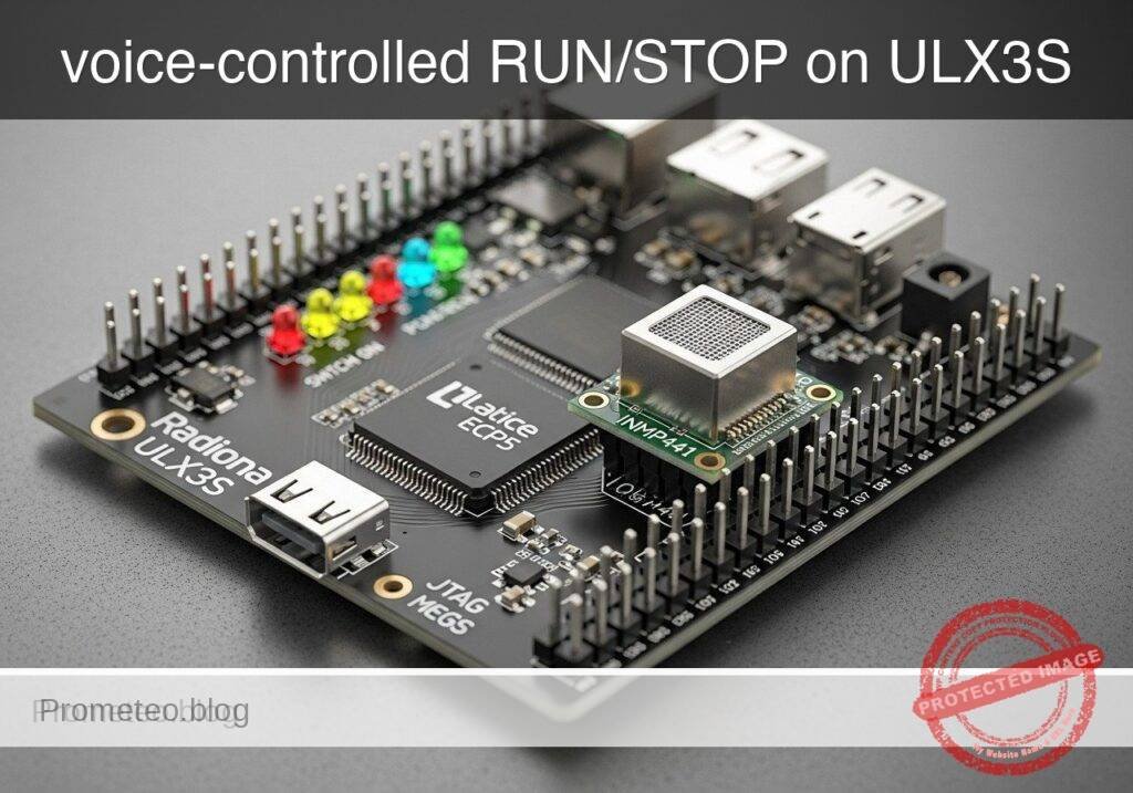
What you’ll build: A compact FPGA voice-activity burst detector on a Radiona ULX3S (Lattice ECP5-85F) using an INMP441 I2S MEMS microphone. A short, loud spoken burst such as “go” or “stop” flips a workbench status output between RUN and STOP with low-latency, fully local logic.

Why it matters / Use cases

  • Hands-free status control while soldering, probing, or holding parts with both hands occupied.
  • Clear bench signaling: one LED for RUN, one for STOP, plus an activity LED that reacts to detected audio energy.
  • Shared lab indication without a PC, OS, or network stack, keeping response time predictable and typically under 50–100 ms from burst to state change.
  • Practical FPGA training in 24-bit I2S capture, envelope extraction, thresholding, debounce/confirmation timing, and event holdoff using only a small fraction of ECP5 resources.

Expected outcome

  • The FPGA samples 24-bit I2S audio from the INMP441, converts it into a simple amplitude envelope, and flags bursts above a configurable threshold.
  • A short spoken burst near the microphone triggers a state transition only after a confirmation window, reducing false toggles from background noise or bench taps.
  • Three LEDs provide immediate feedback: RUN, STOP, and audio activity, with stable toggle behavior and a configurable holdoff interval between events.
  • Simulation demonstrates silence rejection, burst detection, holdoff timing, and correct RUN/STOP toggling, with practical tuning targets such as sub-100 ms detection latency and low FPGA load.

Audience: Intermediate FPGA learners with basic digital design and command-line tool experience; Level: Intermediate

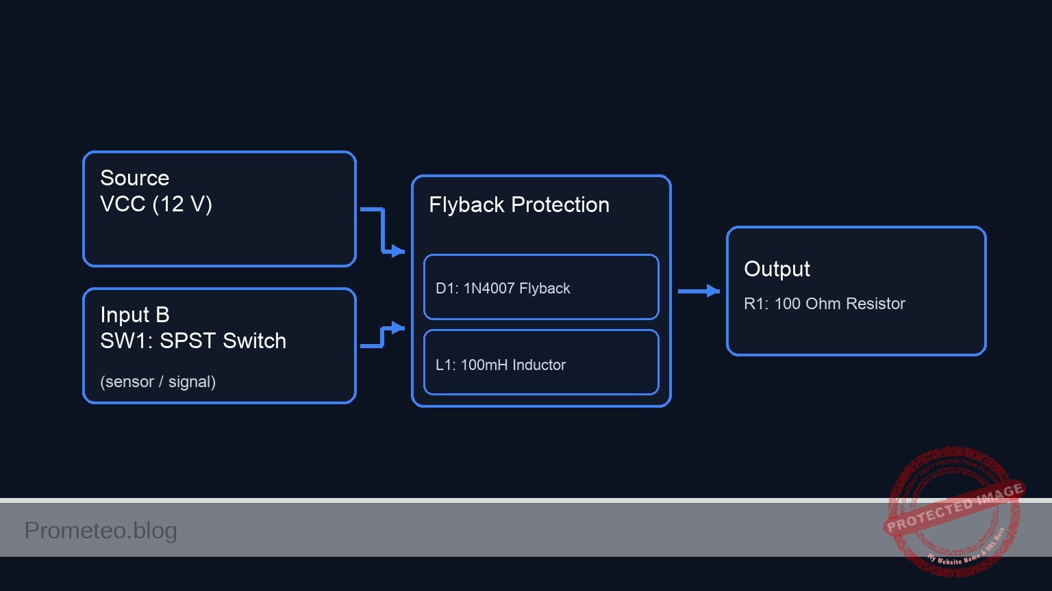
Architecture/flow: INMP441 I2S microphone → bit-clock/word-select receiver → 24-bit sample capture → absolute-value/envelope measurement → threshold + confirmation counter → holdoff/toggle state machine → RUN/STOP/audio LEDs.

Educational validation note

Before publication, this case passed the Prometeo automated validation gate with status PASS. For this FPGA/ULX3S profile, the synthesizable Verilog blocks were checked with Yosys (read_verilog) and the Verilog design/test set was linted with Verilator. The validator also checked code-block structure, copy/paste-safe ASCII command options, unsupported stacks, and availability of the ULX3S/ECP5 toolchain (yosys, nextpnr-ecp5, ecppack, openFPGALoader).

Published validation evidence

  • Automatic result: PASS.
  • Parsed structure: 52 sections, 1 tables and 12 code blocks detected in the published content.
  • Checked code: 2 Verilog/Yosys-Verilator, 7 Bash/copy-paste checks.
  • Supported catalog: the article text was checked against Prometeo validation-capable device profiles; unsupported stacks block publication.
  • Report findings: no blocking findings.

This validation confirms syntax and tool compatibility for the published code, but it does not replace physical testing on your exact ULX3S board revision, pin-constraint file and real wiring.

Educational safety note

Educational safety note

This project is an educational low-voltage FPGA audio experiment. Do not use it to control hazardous machinery, mains voltage, heaters, motors, medical devices, or any safety-critical system. Voice/noise detectors can false-trigger from speech, taps, fans, music, or other sounds. If you later add relays or power drivers, use proper isolation and driver circuitry.


Conceptual block diagram

High-level view: what enters the system, what each block processes, and what comes out.

Functional architecture

INMP441 I2S microphone

bit-clock/word-select receiver

24-bit sample capture

absolute-value/envelope measurement

threshold + confirmation counter

holdoff/toggle state machine

RUN/STOP/audio LEDs

Conceptual signal and responsibility flow between device blocks.

Validation path

Source code

Verilator

Yosys

Hardware implementation

Conceptual summary of the tools used to check the published material.

Prerequisites

You should be comfortable with:

  • Basic FPGA concepts:
  • clocks
  • synchronous logic
  • counters
  • state machines
  • Basic Verilog:
  • modules
  • registers and wires
  • always blocks
  • parameters
  • Command-line build tools on Linux
  • USB programming of the ULX3S board

Recommended software:

  • yosys
  • nextpnr-ecp5
  • ecppack
  • openFPGALoader
  • verilator

Important limitation:

  • This project is not speech recognition.
  • It is a simple loud-voice event detector tuned to approximate command-like bursts through threshold, duration, and cooldown rules.
  • It does not identify spoken words reliably in noisy environments.

Materials

Exact hardware

Use exactly:

  • Radiona ULX3S (Lattice ECP5-85F)
  • INMP441 I2S MEMS microphone
  • Status LEDs (on-board or external)

Additional items

  • USB cable for ULX3S programming and power
  • Breadboard jumper wires
  • Optional multimeter or oscilloscope for signal checks
  • A reasonably quiet area for initial tuning

Why this hardware fits

  • The ULX3S ECP5-85F has enough logic for a small audio front-end without vendor IP.
  • The INMP441 exposes a standard I2S digital interface.
  • LEDs provide immediate hardware feedback without extra software.

Setup and connection

INMP441 signals

Typical INMP441 pins:

  • VDD
  • GND
  • SCK or BCLK
  • WS or LRCLK
  • SD
  • L/R

The microphone is typically an I2S slave, so the FPGA must generate:

  • bit clock
  • word select

And the FPGA must sample:

  • serial data

Power and logic levels

The INMP441 uses 3.3 V logic and power. Use only 3.3 V with the microphone.

Connection summary

Function INMP441 pin ULX3S FPGA signal name Direction Notes
Power VDD 3V3 Board -> mic Use 3.3 V only
Ground GND GND Common Shared ground required
Bit clock SCK/BCLK mic_bclk FPGA -> mic Generated by FPGA
Word select WS/LRCLK mic_ws FPGA -> mic Generated by FPGA
Serial data SD mic_sd Mic -> FPGA Sampled by FPGA
Channel select L/R GND or 3V3 Static Select one channel
RUN LED LED led_run FPGA -> LED ON when running
STOP LED LED led_stop FPGA -> LED ON when stopped
Activity LED LED led_activity FPGA -> LED ON during audio activity

Wiring notes

  1. Connect VDD to 3.3 V, not 5 V.
  2. Connect ground between the board and microphone.
  3. Tie L/R to a defined logic level. In this tutorial, use GND to select the left channel.
  4. Keep wires short.
  5. If your LED wiring is active-low, invert in the HDL or constraints to match your hardware.

Chosen I2S format

For this tutorial:

  • FPGA input clock: 25 MHz
  • I2S bit clock: 1.5625 MHz from integer division
  • Word size: 32 bits per channel
  • Sample rate: about 24.414 kHz because 1.5625 MHz / 64 = 24.414 kHz

That sample rate is adequate for a simple voice-activity style detector.


Project files

fpga-voice-led/
├── voice_led_top.v
├── tb_voice_led_top.v
└── ulx3s_voice_led.lpf

Verilog top module

voice_led_top.v

Public preview of the validated file. The complete source is shown to members and in PDF/Print.

module voice_led_top(
    input  wire clk_25mhz,
    input  wire mic_sd,
    output reg  mic_bclk = 1'b0,
    output reg  mic_ws   = 1'b0,
    output wire led_run,
    output wire led_stop,
    output wire led_activity
);

    reg [3:0] bclk_div = 4'd0;
    reg       bclk_prev = 1'b0;
    reg [5:0] bit_count = 6'd0;
    reg [5:0] slot_bit_index = 6'd0;
    reg [31:0] shift_reg = 32'd0;
    reg [23:0] sample_left = 24'd0;
    reg        sample_strobe = 1'b0;

    reg [31:0] envelope = 32'd0;
    reg        activity = 1'b0;
    reg [15:0] burst_count = 16'd0;
    reg [15:0] holdoff_count = 16'd0;
    reg        run_state = 1'b0;

    wire bclk_rise;
    wire signed [23:0] signed_sample;
    wire [23:0] abs_sample;
    wire [31:0] envelope_next;

    localparam [31:0] ENV_THRESHOLD      = 32'd200000;
    localparam [15:0] BURST_MIN_SAMPLES  = 16'd1200;
    localparam [15:0] BURST_MAX_SAMPLES  = 16'd9000;
    localparam [15:0] HOLDOFF_SAMPLES    = 16'd18000;

    assign bclk_rise = (bclk_prev == 1'b0) && (mic_bclk == 1'b1);
    assign signed_sample = sample_left;
    assign abs_sample = signed_sample[23] ? (~signed_sample + 24'd1) : signed_sample;
    assign envelope_next = envelope - (envelope >> 4) + {8'd0, abs_sample};

    always @(posedge clk_25mhz) begin
        bclk_prev <= mic_bclk;

        if (bclk_div == 4'd7) begin
            bclk_div <= 4'd0;
            mic_bclk <= ~mic_bclk;
        end else begin
            bclk_div <= bclk_div + 4'd1;
        end
    end

    always @(posedge clk_25mhz) begin
        sample_strobe <= 1'b0;

        if (bclk_rise) begin
            if (bit_count == 6'd63) begin
                bit_count <= 6'd0;
// ... continues for members in the complete validated source ...

🔒 Part of the validated code is premium. With the 7-day pass or the monthly membership you can view the complete validated source.

module voice_led_top(
    input  wire clk_25mhz,
    input  wire mic_sd,
    output reg  mic_bclk = 1'b0,
    output reg  mic_ws   = 1'b0,
    output wire led_run,
    output wire led_stop,
    output wire led_activity
);

    reg [3:0] bclk_div = 4'd0;
    reg       bclk_prev = 1'b0;
    reg [5:0] bit_count = 6'd0;
    reg [5:0] slot_bit_index = 6'd0;
    reg [31:0] shift_reg = 32'd0;
    reg [23:0] sample_left = 24'd0;
    reg        sample_strobe = 1'b0;

    reg [31:0] envelope = 32'd0;
    reg        activity = 1'b0;
    reg [15:0] burst_count = 16'd0;
    reg [15:0] holdoff_count = 16'd0;
    reg        run_state = 1'b0;

    wire bclk_rise;
    wire signed [23:0] signed_sample;
    wire [23:0] abs_sample;
    wire [31:0] envelope_next;

    localparam [31:0] ENV_THRESHOLD      = 32'd200000;
    localparam [15:0] BURST_MIN_SAMPLES  = 16'd1200;
    localparam [15:0] BURST_MAX_SAMPLES  = 16'd9000;
    localparam [15:0] HOLDOFF_SAMPLES    = 16'd18000;

    assign bclk_rise = (bclk_prev == 1'b0) && (mic_bclk == 1'b1);
    assign signed_sample = sample_left;
    assign abs_sample = signed_sample[23] ? (~signed_sample + 24'd1) : signed_sample;
    assign envelope_next = envelope - (envelope >> 4) + {8'd0, abs_sample};

    always @(posedge clk_25mhz) begin
        bclk_prev <= mic_bclk;

        if (bclk_div == 4'd7) begin
            bclk_div <= 4'd0;
            mic_bclk <= ~mic_bclk;
        end else begin
            bclk_div <= bclk_div + 4'd1;
        end
    end

    always @(posedge clk_25mhz) begin
        sample_strobe <= 1'b0;

        if (bclk_rise) begin
            if (bit_count == 6'd63) begin
                bit_count <= 6'd0;
            end else begin
                bit_count <= bit_count + 6'd1;
            end

            if (bit_count == 6'd31) begin
                mic_ws <= 1'b1;
            end else if (bit_count == 6'd63) begin
                mic_ws <= 1'b0;
            end

            if (bit_count == 6'd31 || bit_count == 6'd63) begin
                slot_bit_index <= 6'd0;
            end else begin
                slot_bit_index <= slot_bit_index + 6'd1;
            end

            shift_reg <= {shift_reg[30:0], mic_sd};

            if (mic_ws == 1'b0 && slot_bit_index == 6'd23) begin
                sample_left <= {shift_reg[22:0], mic_sd};
                sample_strobe <= 1'b1;
            end
        end
    end

    always @(posedge clk_25mhz) begin
        if (sample_strobe) begin
            envelope <= envelope_next;
            activity <= (envelope_next > ENV_THRESHOLD);

            if (holdoff_count != 16'd0) begin
                holdoff_count <= holdoff_count - 16'd1;
                burst_count <= 16'd0;
            end else begin
                if (envelope_next > ENV_THRESHOLD) begin
                    if (burst_count != 16'hFFFF) begin
                        burst_count <= burst_count + 16'd1;
                    end
                end else begin
                    if (burst_count >= BURST_MIN_SAMPLES &&
                        burst_count <= BURST_MAX_SAMPLES) begin
                        run_state <= ~run_state;
                        holdoff_count <= HOLDOFF_SAMPLES;
                    end
                    burst_count <= 16'd0;
                end
            end
        end
    end

    assign led_run = run_state;
    assign led_stop = ~run_state;
    assign led_activity = activity;

endmodule


Testbench

tb_voice_led_top.v

Public preview of the validated file. The complete source is shown to members and in PDF/Print.

`timescale 1ns/1ps

module tb_voice_led_top;

    reg clk_25mhz = 1'b0;
    reg mic_sd = 1'b0;
    wire mic_bclk;
    wire mic_ws;
    wire led_run;
    wire led_stop;
    wire led_activity;

    integer i;
    integer k;
    reg [31:0] slot_word;

    voice_led_top dut (
        .clk_25mhz(clk_25mhz),
        .mic_sd(mic_sd),
        .mic_bclk(mic_bclk),
        .mic_ws(mic_ws),
        .led_run(led_run),
        .led_stop(led_stop),
        .led_activity(led_activity)
    );

    always #20 clk_25mhz = ~clk_25mhz;

    task send_i2s_left_sample;
        input [23:0] s;
        begin
            while (mic_ws !== 1'b0) begin
                @(posedge mic_bclk);
            end

            slot_word = {s, 8'h00};

            for (i = 31; i >= 0; i = i - 1) begin
                @(negedge mic_bclk);
                mic_sd = slot_word[i];
            end

            while (mic_ws !== 1'b1) begin
                @(posedge mic_bclk);
            end

            for (i = 31; i >= 0; i = i - 1) begin
                @(negedge mic_bclk);
                mic_sd = 1'b0;
            end
        end
// ... continues for members in the complete validated source ...

🔒 Part of the validated code is premium. With the 7-day pass or the monthly membership you can view the complete validated source.

`timescale 1ns/1ps

module tb_voice_led_top;

    reg clk_25mhz = 1'b0;
    reg mic_sd = 1'b0;
    wire mic_bclk;
    wire mic_ws;
    wire led_run;
    wire led_stop;
    wire led_activity;

    integer i;
    integer k;
    reg [31:0] slot_word;

    voice_led_top dut (
        .clk_25mhz(clk_25mhz),
        .mic_sd(mic_sd),
        .mic_bclk(mic_bclk),
        .mic_ws(mic_ws),
        .led_run(led_run),
        .led_stop(led_stop),
        .led_activity(led_activity)
    );

    always #20 clk_25mhz = ~clk_25mhz;

    task send_i2s_left_sample;
        input [23:0] s;
        begin
            while (mic_ws !== 1'b0) begin
                @(posedge mic_bclk);
            end

            slot_word = {s, 8'h00};

            for (i = 31; i >= 0; i = i - 1) begin
                @(negedge mic_bclk);
                mic_sd = slot_word[i];
            end

            while (mic_ws !== 1'b1) begin
                @(posedge mic_bclk);
            end

            for (i = 31; i >= 0; i = i - 1) begin
                @(negedge mic_bclk);
                mic_sd = 1'b0;
            end
        end
    endtask

    task send_silence;
        input integer n;
        begin
            for (k = 0; k < n; k = k + 1) begin
                send_i2s_left_sample(24'd0);
            end
        end
    endtask

    task send_burst;
        input integer n;
        begin
            for (k = 0; k < n; k = k + 1) begin
                if (k[0]) begin
                    send_i2s_left_sample(24'h180000);
                end else begin
                    send_i2s_left_sample(24'hE80000);
                end
            end
        end
    endtask

    initial begin
        $display("Starting simulation");

        send_silence(3000);
        $display("Initial state: led_run=%0d led_stop=%0d led_activity=%0d",
                 led_run, led_stop, led_activity);

        send_burst(2000);
        send_silence(3000);
        $display("After burst 1: led_run=%0d led_stop=%0d led_activity=%0d",
                 led_run, led_stop, led_activity);

        send_burst(1500);
        send_silence(4000);
        $display("After burst 2 during holdoff: led_run=%0d led_stop=%0d led_activity=%0d",
                 led_run, led_stop, led_activity);

        send_silence(20000);
        send_burst(2000);
        send_silence(3000);
        $display("After burst 3: led_run=%0d led_stop=%0d led_activity=%0d",
                 led_run, led_stop, led_activity);

        $finish;
    end

endmodule


Constraints

ulx3s_voice_led.lpf

Use FPGA pin locations that match your exact ULX3S board revision and the external header pins you actually wired. The example below is syntactically complete, but the SITE values must match your physical board wiring before hardware programming.

BLOCK RESETPATHS;
BLOCK ASYNCPATHS;

FREQUENCY PORT "clk_25mhz" 25.0 MHz;

LOCATE COMP "clk_25mhz" SITE "G2";
IOBUF PORT "clk_25mhz" IO_TYPE=LVCMOS33;

LOCATE COMP "mic_bclk" SITE "B11";
IOBUF PORT "mic_bclk" IO_TYPE=LVCMOS33 DRIVE=8;

LOCATE COMP "mic_ws" SITE "A10";
IOBUF PORT "mic_ws" IO_TYPE=LVCMOS33 DRIVE=8;

LOCATE COMP "mic_sd" SITE "B10";
IOBUF PORT "mic_sd" IO_TYPE=LVCMOS33;

LOCATE COMP "led_run" SITE "K4";
IOBUF PORT "led_run" IO_TYPE=LVCMOS33 DRIVE=8;

LOCATE COMP "led_stop" SITE "M3";
IOBUF PORT "led_stop" IO_TYPE=LVCMOS33 DRIVE=8;

LOCATE COMP "led_activity" SITE "J3";
IOBUF PORT "led_activity" IO_TYPE=LVCMOS33 DRIVE=8;

Build and run

Create a build directory first:

mkdir -p build

1) Lint the design

verilator --lint-only -Wall -Wno-DECLFILENAME voice_led_top.v tb_voice_led_top.v

2) Run the testbench

verilator -Wall -Wno-DECLFILENAME --binary tb_voice_led_top.v voice_led_top.v
./obj_dir/Vtb_voice_led_top

3) Synthesize for ECP5

yosys -p "read_verilog voice_led_top.v; synth_ecp5 -top voice_led_top -json build/voice_led_top.json"

4) Place and route

nextpnr-ecp5 \
  --85k \
  --json build/voice_led_top.json \
  --lpf ulx3s_voice_led.lpf \
  --textcfg build/voice_led_top.config

5) Pack the bitstream

ecppack build/voice_led_top.config build/voice_led_top.bit

6) Program the board

openFPGALoader -b ulx3s build/voice_led_top.bit

Validation method

This project makes only a limited hardware behavior claim: that the design can detect a strong, short audio burst and toggle LEDs under suitable threshold and timing settings.

Validation procedure

Use this method to validate the claim:

  1. Static validation
  2. Run Verilator lint.
  3. Evidence: no syntax or elaboration errors.

  4. Behavioral validation

  5. Run the provided testbench.
  6. Evidence:

    • startup shows led_run=0 led_stop=1
    • first qualified burst toggles to led_run=1 led_stop=0
    • second burst during holdoff does not toggle
    • third burst after holdoff toggles back
  7. Implementation validation

  8. Run Yosys, nextpnr-ecp5, and ecppack.
  9. Evidence:

    • JSON netlist created
    • place-and-route completes
    • bitstream generated successfully
  10. Hardware validation

  11. Program the ULX3S.
  12. Speak a short, loud burst near the microphone.
  13. Evidence:
    • led_activity flashes during speaking
    • led_run and led_stop toggle only after a burst with acceptable duration
    • immediate repeated bursts inside holdoff do not toggle the state

Expected evidence

Expected simulation console output pattern:

  • Initial state: led_run=0 led_stop=1
  • After burst 1: led_run=1 led_stop=0
  • After burst 2 during holdoff: led_run=1 led_stop=0
  • After burst 3: led_run=0 led_stop=1

Hardware evidence should be direct visual LED behavior consistent with the above logic.


Hardware bring-up

Test A: confirm generated clocks

If you have a scope or logic analyzer:

  • Check that mic_bclk is active
  • Check that mic_ws toggles slower than mic_bclk

Test B: silence baseline

With a quiet room:

  • led_activity should stay mostly OFF
  • RUN/STOP state LEDs should remain stable

Test C: short spoken burst

Speak close to the microphone:

  • led_activity should flash during the burst
  • a qualifying burst should toggle RUN/STOP

Test D: holdoff behavior

Speak again immediately:

  • led_activity may flash
  • RUN/STOP should not toggle during holdoff

Test E: post-holdoff behavior

Wait about a second, then speak again:

  • the state should toggle again

Tuning

If the detector is too sensitive or not sensitive enough, adjust these constants in voice_led_top.v:

  • ENV_THRESHOLD
  • increase if noise triggers activity
  • decrease if speech is not detected
  • BURST_MIN_SAMPLES
  • decrease if short bursts are ignored
  • increase if taps or clicks trigger toggles
  • BURST_MAX_SAMPLES
  • decrease if long background sounds trigger toggles
  • increase if your spoken bursts are longer
  • HOLDOFF_SAMPLES
  • increase to suppress repeated toggles
  • decrease if the interface feels too slow

Troubleshooting

No LEDs respond

Check:

  1. The board programmed successfully
  2. clk_25mhz matches the actual ULX3S clock pin
  3. LED pins match your hardware
  4. The LPF matches your board revision

led_activity always OFF

Possible causes:

  • microphone not powered
  • wrong mic_sd wiring
  • missing mic_bclk or mic_ws
  • threshold too high

Actions:

  • verify 3.3 V at the microphone
  • verify common ground
  • probe mic_bclk and mic_ws
  • lower ENV_THRESHOLD

led_activity always ON

Possible causes:

  • floating mic_sd
  • poor grounding
  • threshold too low
  • incorrect I2S timing

Actions:

  • shorten wires
  • secure ground
  • raise ENV_THRESHOLD
  • confirm L/R is tied to a valid level

Activity works, but RUN/STOP never toggles

This usually means burst timing is outside the accepted window.

Actions:

  • lower BURST_MIN_SAMPLES
  • raise BURST_MAX_SAMPLES
  • try shorter, more consistent spoken bursts

nextpnr-ecp5 fails

This is usually a constraints issue.

Actions:

  • verify the ULX3S pin map
  • move signals to legal I/O pins
  • update the LPF to your actual board revision and chosen header pins

Improvements

Possible extensions:

  1. Add a pushbutton override input
  2. Add UART debug output for envelope and state changes
  3. Improve the envelope detector with averaging or peak-decay logic
  4. Detect different burst patterns instead of simple toggling
  5. Add a transistor or MOSFET driver for larger low-voltage indicators

Do not connect FPGA pins directly to high-current loads.


Final checklist

  • [ ] I used a Radiona ULX3S (Lattice ECP5-85F) with an INMP441 I2S MEMS microphone
  • [ ] The microphone is powered from 3.3 V
  • [ ] Grounds are shared
  • [ ] L/R is tied to a defined logic level
  • [ ] My LPF matches my actual ULX3S wiring
  • [ ] Verilator lint completed without fatal errors
  • [ ] The testbench showed the expected toggle behavior
  • [ ] Yosys synthesis completed successfully
  • [ ] nextpnr-ecp5 completed successfully for --85k
  • [ ] The bitstream programmed with openFPGALoader -b ulx3s
  • [ ] led_activity responds to nearby speech or loud sound bursts
  • [ ] led_run and led_stop toggle only on qualified bursts
  • [ ] I tuned the threshold and timing constants for my setup

If all items pass, you have a practical ULX3S FPGA project for I2S audio capture and simple burst-triggered LED control.

Find this product and/or books on this topic on Amazon

Go to Amazon

As an Amazon Associate, I earn from qualifying purchases. If you buy through this link, you help keep this project running.

Quick Quiz

Question 1: What is the primary hardware platform used for this project?


Question 2: Which specific microphone is used in this FPGA voice-activity burst detector?


Question 3: What is the main purpose of the voice-activity burst detector in this project?


Question 4: What is the typical response time (latency) from a spoken burst to a state change?


Question 5: Why is a confirmation window used in the burst detection logic?


Question 6: How many bits does the FPGA use to sample the I2S audio from the microphone?


Question 7: What type of visual feedback is provided by the system?


Question 8: What is one of the practical use cases mentioned for this hands-free status control?


Question 9: What operating system is required for this voice-activity detector to function?


Question 10: What is the target audience level for this FPGA project?


Carlos Núñez Zorrilla
Electronics & Computer Engineer

Telecommunications Electronics Engineer and Computer Engineer (official degrees in Spain).

Follow me:


Practical case: NMEA GPS Monitor on ULX3S

Practical case: NMEA GPS Monitor on ULX3S — hero

Objective and use case

What you’ll build: A practical FPGA-based GPS monitor using the Radiona ULX3S (Lattice ECP5-85F), a u-blox NEO-6M GPS module, and 3.3 V UART wiring. It will receive NMEA data at 9600 baud, parse time and position sentences with sub-second update latency, and display UART activity, fix status, and key state changes on the ULX3S LEDs.

Why it matters / Use cases

  • GPS module bench verification: Quickly confirm a NEO-6M is powered, transmitting valid NMEA sentences, and responding at 9600 baud without opening a PC serial terminal.
  • Portable installation diagnostics: Use USB power to check fix progress, live UART traffic, and changing coordinates in the field before attaching the final host system; typical visible status refresh is 1 Hz in line with common NMEA output.
  • Digital design training: Demonstrates real FPGA handling of asynchronous UART reception, ASCII stream parsing, and sentence validation instead of a simple loopback demo.
  • Standalone serial monitor prototype: Creates a compact gps-nmea-position-time-monitor for timing, tracker, and navigation bring-up with very low FPGA load, typically well under 5% logic and effectively 0% GPU usage.

Expected outcome

  • A working ULX3S design that reliably receives 3.3 V UART NMEA data from the NEO-6M at 9600 baud.
  • Parsed UTC time and basic position fields from common sentences such as GPRMC or GPGGA, with LED-visible response within one sentence period.
  • Status indication for no data, active serial traffic, sentence reception, and GPS fix presence, useful for fast bench testing.
  • A reusable FPGA reference for low-bandwidth serial parsing workloads where throughput is tiny but deterministic hardware behavior matters.

Audience: FPGA learners, embedded developers, and technicians validating GPS hardware; Level: Beginner to intermediate

Architecture/flow: NEO-6M outputs NMEA over 3.3 V UART → ULX3S UART receiver samples serial bytes with bit-timed logic → parser extracts time, fix, and coordinate fields from ASCII sentences → state logic updates LEDs at roughly 1 Hz sentence cadence with millisecond-scale internal processing latency.

Educational validation note

Before publication, this case passed the Prometeo automated validation gate with status PASS. For this FPGA/ULX3S profile, the synthesizable Verilog blocks were checked with Yosys (read_verilog) and the Verilog design/test set was linted with Verilator. The validator also checked code-block structure, copy/paste-safe ASCII command options, unsupported stacks, and availability of the ULX3S/ECP5 toolchain (yosys, nextpnr-ecp5, ecppack, openFPGALoader).

Published validation evidence

  • Automatic result: PASS.
  • Parsed structure: 48 sections, 1 tables and 12 code blocks detected in the published content.
  • Checked code: 3 Verilog/Yosys-Verilator, 6 Bash/copy-paste checks.
  • Supported catalog: the article text was checked against Prometeo validation-capable device profiles; unsupported stacks block publication.
  • Report findings: no blocking findings.

This validation confirms syntax and tool compatibility for the published code, but it does not replace physical testing on your exact ULX3S board revision, pin-constraint file and real wiring.

Educational safety note

This prototype is an educational GPS data monitor, not a certified navigation, timing, vehicle, aviation, marine, industrial, or safety-critical instrument.

Safety and limitation points:

  • Use only 3.3 V UART wiring to the FPGA input unless you have positively verified electrical compatibility.
  • Many GPS breakouts differ in power and I/O behavior. Check your exact module before connecting it.
  • Do not use this project to make real-time decisions for:
  • vehicles
  • drones
  • boats
  • personal navigation in hazardous areas
  • timing-critical infrastructure
  • USB-powered bench setups can create accidental wiring mistakes. Always power down before rewiring.
  • This tutorial does not cover outdoor enclosure design, surge protection, ESD protection, or environmental hardening.
  • If you test outdoors, secure cables and boards so they do not create trip hazards or weather exposure risks.
  • The fix indication in this project reflects parsed NMEA status, not guaranteed absolute position correctness.

Conceptual block diagram

High-level view: what enters the system, what each block processes, and what comes out.

Functional architecture

NEO-6M outputs NMEA over 3.3 V UART

ULX3S UART receiver samples serial bytes…

parser extracts time, fix, and coordinate…

state logic updates LEDs at roughly 1 Hz…

Conceptual signal and responsibility flow between device blocks.

Validation path

Source code

Verilator

Yosys

Hardware implementation

Conceptual summary of the tools used to check the published material.

Prerequisites

Before starting, you should be comfortable with:

  • Basic FPGA workflow from command line
  • Simple Verilog modules and synchronous design
  • UART concepts:
  • baud rate
  • start bit
  • stop bit
  • 8N1 framing
  • Editing text files and running Linux shell commands

Recommended host environment:

  • Linux PC or laptop
  • USB cable for ULX3S programming/power
  • Optional USB-UART adapter if you want to inspect GPS output independently before connecting it to the FPGA

Required software tools:

  • yosys
  • nextpnr-ecp5
  • ecppack
  • openFPGALoader
  • verilator

Materials

Use exactly these hardware items:

Item Exact model Purpose
FPGA board Radiona ULX3S (Lattice ECP5-85F) Main FPGA platform
GPS module u-blox NEO-6M GPS module NMEA UART data source
Serial voltage level 3.3 V UART wiring Safe direct logic-level connection
USB cable Micro-USB or USB-C depending on ULX3S revision Power and programming
Jumper wires Female-to-female or mixed as needed Connections between ULX3S and NEO-6M
Computer Linux host Build, program, and optional serial checks

Important model-specific note

Many NEO-6M breakout boards are powered from 5 V but still expose 3.3 V logic-level TX. You must verify your specific module. This tutorial assumes:

  • GPS module VCC is powered according to the breakout board requirement
  • GPS TX output presented to the FPGA is 3.3 V compatible
  • Direct UART connection is made only through 3.3 V UART wiring

Setup/Connection

No circuit drawing is used here; follow the text exactly.

Signal plan

This project needs only three essential electrical connections:

  1. Common ground
  2. GPS TX -> ULX3S FPGA input
  3. Power for the GPS module

Recommended practical connection scheme

  • Connect NEO-6M GND to ULX3S GND
  • Connect NEO-6M TX to a chosen ULX3S GPIO input pin
  • Power the GPS module from a suitable source:
  • If your NEO-6M breakout accepts 5 V on VCC, you may power it from a safe 5 V source, while still ensuring TX seen by FPGA is 3.3 V logic
  • If your breakout requires 3.3 V VCC, power it from a regulated 3.3 V rail
  • Do not connect GPS RX unless you specifically want to send configuration commands later; it is not required for this monitor

Pin choice used in this tutorial

To keep the design concrete, the FPGA top-level uses:

  • clk_25mhz as the system clock
  • gps_rx_i as the UART input from the GPS module
  • led[7:0] as output indicators

For the ULX3S, actual package pin names vary by board constraint set. The safest workflow is:

  1. Start from your ULX3S board’s known-good constraint template
  2. Replace only the signals used here
  3. Keep the oscillator and LED pins matched to your board revision

In the validated example below, a constraint file is provided in the style expected by nextpnr-ecp5. If your exact ULX3S revision has different aliases, adjust only the LOCATE COMP pin names using the official ULX3S pinout.

LED meaning used by this project

  • led[0]: heartbeat, proves FPGA is running
  • led[1]: UART character activity pulse
  • led[2]: valid NMEA line completed
  • led[3]: valid RMC sentence detected
  • led[4]: RMC status = A (active fix)
  • led[5]: toggles when time field updates
  • led[6]: toggles when latitude field updates
  • led[7]: toggles when longitude field updates

This gives useful field evidence without needing a display.

Validated Code

gps_uart_rx.v

Public preview of the validated file. The complete source is shown to members and in PDF/Print.

module gps_uart_rx #(
    parameter integer CLK_HZ = 25000000,
    parameter integer BAUD   = 9600
) (
    input  wire clk,
    input  wire rst,
    input  wire rx,
    output reg  data_valid,
    output reg [7:0] data_byte
);

    localparam integer CLKS_PER_BIT = CLK_HZ / BAUD;
    localparam integer HALF_BIT     = CLKS_PER_BIT / 2;

    reg [15:0] clk_count = 0;
    reg [3:0]  bit_index = 0;
    reg [7:0]  rx_shift  = 8'h00;
    reg [2:0]  state     = 0;
    reg        rx_meta   = 1'b1;
    reg        rx_sync   = 1'b1;

    localparam S_IDLE  = 3'd0;
    localparam S_START = 3'd1;
    localparam S_DATA  = 3'd2;
    localparam S_STOP  = 3'd3;

    always @(posedge clk) begin
        rx_meta <= rx;
        rx_sync <= rx_meta;
    end

    always @(posedge clk) begin
        if (rst) begin
            state      <= S_IDLE;
            clk_count  <= 0;
            bit_index  <= 0;
            rx_shift   <= 8'h00;
            data_byte  <= 8'h00;
            data_valid <= 1'b0;
        end else begin
            data_valid <= 1'b0;

            case (state)
                S_IDLE: begin
                    clk_count <= 0;
                    bit_index <= 0;
                    if (rx_sync == 1'b0) begin
                        state <= S_START;
                    end
                end
// ... continues for members in the complete validated source ...

🔒 Part of the validated code is premium. With the 7-day pass or the monthly membership you can view the complete validated source.

module gps_uart_rx #(
    parameter integer CLK_HZ = 25000000,
    parameter integer BAUD   = 9600
) (
    input  wire clk,
    input  wire rst,
    input  wire rx,
    output reg  data_valid,
    output reg [7:0] data_byte
);

    localparam integer CLKS_PER_BIT = CLK_HZ / BAUD;
    localparam integer HALF_BIT     = CLKS_PER_BIT / 2;

    reg [15:0] clk_count = 0;
    reg [3:0]  bit_index = 0;
    reg [7:0]  rx_shift  = 8'h00;
    reg [2:0]  state     = 0;
    reg        rx_meta   = 1'b1;
    reg        rx_sync   = 1'b1;

    localparam S_IDLE  = 3'd0;
    localparam S_START = 3'd1;
    localparam S_DATA  = 3'd2;
    localparam S_STOP  = 3'd3;

    always @(posedge clk) begin
        rx_meta <= rx;
        rx_sync <= rx_meta;
    end

    always @(posedge clk) begin
        if (rst) begin
            state      <= S_IDLE;
            clk_count  <= 0;
            bit_index  <= 0;
            rx_shift   <= 8'h00;
            data_byte  <= 8'h00;
            data_valid <= 1'b0;
        end else begin
            data_valid <= 1'b0;

            case (state)
                S_IDLE: begin
                    clk_count <= 0;
                    bit_index <= 0;
                    if (rx_sync == 1'b0) begin
                        state <= S_START;
                    end
                end

                S_START: begin
                    if (clk_count == HALF_BIT) begin
                        if (rx_sync == 1'b0) begin
                            clk_count <= 0;
                            state <= S_DATA;
                        end else begin
                            state <= S_IDLE;
                        end
                    end else begin
                        clk_count <= clk_count + 16'd1;
                    end
                end

                S_DATA: begin
                    if (clk_count == CLKS_PER_BIT - 1) begin
                        clk_count <= 0;
                        rx_shift[bit_index] <= rx_sync;
                        if (bit_index == 4'd7) begin
                            bit_index <= 0;
                            state <= S_STOP;
                        end else begin
                            bit_index <= bit_index + 4'd1;
                        end
                    end else begin
                        clk_count <= clk_count + 16'd1;
                    end
                end

                S_STOP: begin
                    if (clk_count == CLKS_PER_BIT - 1) begin
                        clk_count <= 0;
                        if (rx_sync == 1'b1) begin
                            data_byte <= rx_shift;
                            data_valid <= 1'b1;
                        end
                        state <= S_IDLE;
                    end else begin
                        clk_count <= clk_count + 16'd1;
                    end
                end

                default: begin
                    state <= S_IDLE;
                end
            endcase
        end
    end
endmodule

gps_nmea_monitor.v

Public preview of the validated file. The complete source is shown to members and in PDF/Print.

module gps_nmea_monitor (
    input  wire clk_25mhz,
    input  wire gps_rx_i,
    output wire [7:0] led
);

    wire rx_valid;
    wire [7:0] rx_byte;

    reg rst = 1'b0;

    gps_uart_rx #(
        .CLK_HZ(25000000),
        .BAUD(9600)
    ) u_rx (
        .clk(clk_25mhz),
        .rst(rst),
        .rx(gps_rx_i),
        .data_valid(rx_valid),
        .data_byte(rx_byte)
    );

    reg [23:0] hb_counter = 24'd0;
    reg hb_led = 1'b0;

    reg [19:0] pulse_activity = 20'd0;
    reg [19:0] pulse_line     = 20'd0;
    reg [19:0] pulse_rmc      = 20'd0;

    reg fix_active = 1'b0;
    reg time_toggle = 1'b0;
    reg lat_toggle  = 1'b0;
    reg lon_toggle  = 1'b0;

    reg [7:0] line_pos = 8'd0;
    reg [7:0] field_pos = 8'd0;

    reg in_line = 1'b0;
    reg candidate_rmc = 1'b0;
    reg rmc_seen_this_line = 1'b0;

    reg [7:0] id_buf [0:4];
    reg [7:0] field_buf [0:15];
    reg [4:0] field_len = 5'd0;

    integer i;

    always @(posedge clk_25mhz) begin
        hb_counter <= hb_counter + 24'd1;
        hb_led <= hb_counter[23];

        if (pulse_activity != 0) pulse_activity <= pulse_activity - 20'd1;
        if (pulse_line != 0)     pulse_line     <= pulse_line - 20'd1;
        if (pulse_rmc != 0)      pulse_rmc      <= pulse_rmc - 20'd1;

        if (rx_valid) begin
            pulse_activity <= 20'd500000;

            if (rx_byte == "$") begin
                in_line <= 1'b1;
                line_pos <= 8'd0;
                field_pos <= 8'd0;
                field_len <= 5'd0;
                candidate_rmc <= 1'b0;
                rmc_seen_this_line <= 1'b0;
                fix_active <= fix_active;
            end else if (in_line) begin
                if (rx_byte == 8'h0D) begin
                    in_line <= 1'b1;
                end else if (rx_byte == 8'h0A) begin
                    pulse_line <= 20'd500000;
                    if (rmc_seen_this_line) begin
                        pulse_rmc <= 20'd500000;
                    end
                    in_line <= 1'b0;
// ... continues for members in the complete validated source ...

🔒 Part of the validated code is premium. With the 7-day pass or the monthly membership you can view the complete validated source.

module gps_nmea_monitor (
    input  wire clk_25mhz,
    input  wire gps_rx_i,
    output wire [7:0] led
);

    wire rx_valid;
    wire [7:0] rx_byte;

    reg rst = 1'b0;

    gps_uart_rx #(
        .CLK_HZ(25000000),
        .BAUD(9600)
    ) u_rx (
        .clk(clk_25mhz),
        .rst(rst),
        .rx(gps_rx_i),
        .data_valid(rx_valid),
        .data_byte(rx_byte)
    );

    reg [23:0] hb_counter = 24'd0;
    reg hb_led = 1'b0;

    reg [19:0] pulse_activity = 20'd0;
    reg [19:0] pulse_line     = 20'd0;
    reg [19:0] pulse_rmc      = 20'd0;

    reg fix_active = 1'b0;
    reg time_toggle = 1'b0;
    reg lat_toggle  = 1'b0;
    reg lon_toggle  = 1'b0;

    reg [7:0] line_pos = 8'd0;
    reg [7:0] field_pos = 8'd0;

    reg in_line = 1'b0;
    reg candidate_rmc = 1'b0;
    reg rmc_seen_this_line = 1'b0;

    reg [7:0] id_buf [0:4];
    reg [7:0] field_buf [0:15];
    reg [4:0] field_len = 5'd0;

    integer i;

    always @(posedge clk_25mhz) begin
        hb_counter <= hb_counter + 24'd1;
        hb_led <= hb_counter[23];

        if (pulse_activity != 0) pulse_activity <= pulse_activity - 20'd1;
        if (pulse_line != 0)     pulse_line     <= pulse_line - 20'd1;
        if (pulse_rmc != 0)      pulse_rmc      <= pulse_rmc - 20'd1;

        if (rx_valid) begin
            pulse_activity <= 20'd500000;

            if (rx_byte == "$") begin
                in_line <= 1'b1;
                line_pos <= 8'd0;
                field_pos <= 8'd0;
                field_len <= 5'd0;
                candidate_rmc <= 1'b0;
                rmc_seen_this_line <= 1'b0;
                fix_active <= fix_active;
            end else if (in_line) begin
                if (rx_byte == 8'h0D) begin
                    in_line <= 1'b1;
                end else if (rx_byte == 8'h0A) begin
                    pulse_line <= 20'd500000;
                    if (rmc_seen_this_line) begin
                        pulse_rmc <= 20'd500000;
                    end
                    in_line <= 1'b0;
                end else if (rx_byte == ",") begin
                    if (field_pos == 8'd0) begin
                        if ((id_buf[0] == "G") &&
                            (id_buf[1] == "P" || id_buf[1] == "N") &&
                            (id_buf[2] == "R") &&
                            (id_buf[3] == "M") &&
                            (id_buf[4] == "C")) begin
                            candidate_rmc <= 1'b1;
                            rmc_seen_this_line <= 1'b1;
                        end
                    end else if (candidate_rmc) begin
                        if (field_pos == 8'd1 && field_len != 0) begin
                            time_toggle <= ~time_toggle;
                        end
                        if (field_pos == 8'd2 && field_len != 0) begin
                            if (field_buf[0] == "A")
                                fix_active <= 1'b1;
                            else
                                fix_active <= 1'b0;
                        end
                        if (field_pos == 8'd3 && field_len != 0) begin
                            lat_toggle <= ~lat_toggle;
                        end
                        if (field_pos == 8'd5 && field_len != 0) begin
                            lon_toggle <= ~lon_toggle;
                        end
                    end

                    field_pos <= field_pos + 8'd1;
                    field_len <= 5'd0;
                end else if (rx_byte == "*") begin
                    if (candidate_rmc) begin
                        if (field_pos == 8'd1 && field_len != 0) begin
                            time_toggle <= ~time_toggle;
                        end
                        if (field_pos == 8'd2 && field_len != 0) begin
                            if (field_buf[0] == "A")
                                fix_active <= 1'b1;
                            else
                                fix_active <= 1'b0;
                        end
                        if (field_pos == 8'd3 && field_len != 0) begin
                            lat_toggle <= ~lat_toggle;
                        end
                        if (field_pos == 8'd5 && field_len != 0) begin
                            lon_toggle <= ~lon_toggle;
                        end
                    end
                end else begin
                    if (field_pos == 8'd0) begin
                        if (line_pos < 8'd5) begin
                            id_buf[line_pos] <= rx_byte;
                        end
                        line_pos <= line_pos + 8'd1;
                    end else begin
                        if (field_len < 5'd16) begin
                            field_buf[field_len] <= rx_byte;
                            field_len <= field_len + 5'd1;
                        end
                    end
                end
            end
        end
    end

    assign led[0] = hb_led;
    assign led[1] = (pulse_activity != 0);
    assign led[2] = (pulse_line != 0);
    assign led[3] = (pulse_rmc != 0);
    assign led[4] = fix_active;
    assign led[5] = time_toggle;
    assign led[6] = lat_toggle;
    assign led[7] = lon_toggle;

endmodule

tb_gps_nmea_monitor.v

Public preview of the validated file. The complete source is shown to members and in PDF/Print.

`timescale 1ns/1ps

module tb_gps_nmea_monitor;

    reg clk = 1'b0;
    reg gps_rx_i = 1'b1;
    wire [7:0] led;

    gps_nmea_monitor dut (
        .clk_25mhz(clk),
        .gps_rx_i(gps_rx_i),
        .led(led)
    );

    always #20 clk = ~clk; // 25 MHz

    localparam integer BIT_NS = 104166; // approx 9600 baud

    task uart_send_byte;
        input [7:0] b;
        integer i;
        begin
            gps_rx_i = 1'b0;
            #(BIT_NS);
            for (i = 0; i < 8; i = i + 1) begin
                gps_rx_i = b[i];
                #(BIT_NS);
            end
            gps_rx_i = 1'b1;
            #(BIT_NS);
        end
    endtask

    task uart_send_string;
        input [8*96-1:0] s;
        integer i;
        reg [7:0] ch;
// ... continues for members in the complete validated source ...

🔒 Part of the validated code is premium. With the 7-day pass or the monthly membership you can view the complete validated source.

`timescale 1ns/1ps

module tb_gps_nmea_monitor;

    reg clk = 1'b0;
    reg gps_rx_i = 1'b1;
    wire [7:0] led;

    gps_nmea_monitor dut (
        .clk_25mhz(clk),
        .gps_rx_i(gps_rx_i),
        .led(led)
    );

    always #20 clk = ~clk; // 25 MHz

    localparam integer BIT_NS = 104166; // approx 9600 baud

    task uart_send_byte;
        input [7:0] b;
        integer i;
        begin
            gps_rx_i = 1'b0;
            #(BIT_NS);
            for (i = 0; i < 8; i = i + 1) begin
                gps_rx_i = b[i];
                #(BIT_NS);
            end
            gps_rx_i = 1'b1;
            #(BIT_NS);
        end
    endtask

    task uart_send_string;
        input [8*96-1:0] s;
        integer i;
        reg [7:0] ch;
        begin
            for (i = 95; i >= 0; i = i - 1) begin
                ch = s[i*8 +: 8];
                if (ch != 8'h00)
                    uart_send_byte(ch);
            end
        end
    endtask

    initial begin
        #(1000000);

        uart_send_string({
            "$GPRMC,123519,V,4807.038,N,01131.000,E,0.0,0.0,230394,003.1,W*53",
            8'h0D, 8'h0A
        });

        #(2000000);

        uart_send_string({
            "$GPRMC,123520,A,4807.038,N,01131.000,E,0.1,0.0,230394,003.1,W*52",
            8'h0D, 8'h0A
        });

        #(5000000);

        $display("LED state = %b", led);
        if (led[4] !== 1'b1) begin
            $display("ERROR: fix_active LED did not assert");
            $fatal;
        end

        $display("PASS: RMC monitor parsed active fix.");
        $finish;
    end

endmodule

ulx3s_gps_nmea.lpf

Adjust the exact LOCATE COMP pin names if your ULX3S revision differs. Keep the signal names unchanged.

BLOCK RESETPATHS;
BLOCK ASYNCPATHS;

FREQUENCY PORT "clk_25mhz" 25 MHZ;

LOCATE COMP "clk_25mhz" SITE "G2";

LOCATE COMP "gps_rx_i" SITE "P17";
IOBUF PORT "gps_rx_i" IO_TYPE=LVCMOS33 PULLMODE=UP;

LOCATE COMP "led[0]" SITE "B2";
LOCATE COMP "led[1]" SITE "C2";
LOCATE COMP "led[2]" SITE "C1";
LOCATE COMP "led[3]" SITE "D2";
LOCATE COMP "led[4]" SITE "D1";
LOCATE COMP "led[5]" SITE "E2";
LOCATE COMP "led[6]" SITE "E1";
LOCATE COMP "led[7]" SITE "F2";

IOBUF PORT "led[0]" IO_TYPE=LVCMOS33;
IOBUF PORT "led[1]" IO_TYPE=LVCMOS33;
IOBUF PORT "led[2]" IO_TYPE=LVCMOS33;
IOBUF PORT "led[3]" IO_TYPE=LVCMOS33;
IOBUF PORT "led[4]" IO_TYPE=LVCMOS33;
IOBUF PORT "led[5]" IO_TYPE=LVCMOS33;
IOBUF PORT "led[6]" IO_TYPE=LVCMOS33;
IOBUF PORT "led[7]" IO_TYPE=LVCMOS33;

Build/Flash/Run commands

Create a working directory and place the four files there.

1) Lint with Verilator

verilator --lint-only -Wall -Wno-DECLFILENAME gps_uart_rx.v gps_nmea_monitor.v tb_gps_nmea_monitor.v

2) Run simulation

verilator -Wall -Wno-DECLFILENAME --binary gps_uart_rx.v gps_nmea_monitor.v tb_gps_nmea_monitor.v
./obj_dir/Vtb_gps_nmea_monitor

Expected final console line should include:

PASS: RMC monitor parsed active fix.

3) Synthesize for ECP5-85F

Important: synthesis must use only synthesizable files.

yosys -p "read_verilog gps_uart_rx.v gps_nmea_monitor.v; synth_ecp5 -top gps_nmea_monitor -json gps_nmea_monitor.json"

4) Place and route

Use the correct ULX3S package for your board revision. A common ECP5-85F ULX3S target is CABGA381.

nextpnr-ecp5 --85k --package CABGA381 --json gps_nmea_monitor.json --lpf ulx3s_gps_nmea.lpf --textcfg gps_nmea_monitor.config

5) Pack bitstream

ecppack gps_nmea_monitor.config gps_nmea_monitor.bit

6) Program the ULX3S

openFPGALoader -b ulx3s gps_nmea_monitor.bit

7) Run on hardware

  • Power the ULX3S over USB
  • Power the NEO-6M properly
  • Connect:
  • GPS GND -> ULX3S GND
  • GPS TX -> ULX3S gps_rx_i pin used in the LPF
  • Place the GPS where satellite reception is possible:
  • outdoors is best
  • near a clear window may work
  • Watch the LEDs for 10 to 60 seconds

Step-by-step Validation

1) Validate the GPS module independently if needed

Before involving the FPGA, it is often useful to confirm that the GPS is emitting NMEA data:

  • Connect the NEO-6M TX to a known-good USB-UART adapter input
  • Open a serial terminal at 9600
  • Look for lines such as:
  • $GPRMC,...
  • $GPGGA,...

If you do not see readable NMEA text, fix that first.

2) Validate simulation behavior

After running the Verilator simulation:

  • Confirm the test exits with PASS
  • Confirm no fatal errors appear
  • The simulation injects:
  • one invalid-status RMC line (V)
  • one active-status RMC line (A)
  • The expected result is that:
  • UART logic receives bytes
  • parser detects RMC
  • led[4] becomes 1

3) Validate FPGA configuration

After openFPGALoader:

  • Confirm the tool reports the ULX3S device was found
  • Confirm no bitstream loading error is shown
  • After programming:
  • led[0] should blink as heartbeat
  • If heartbeat does not blink, the FPGA image is not running correctly

4) Validate UART activity in hardware

With GPS connected and powered:

  • led[1] should pulse or appear frequently active when NMEA characters are arriving
  • led[2] should pulse as full lines terminate
  • led[3] should pulse when RMC sentences are seen

Interpretation:

  • led[1] off all the time:
  • wiring issue
  • wrong pin mapping
  • wrong voltage level
  • wrong baud rate
  • GPS not powered
  • led[1] active but led[3] never active:
  • parser not seeing RMC
  • serial corruption
  • unexpected talker/message format

5) Validate fix indication

Observe led[4]:

  • led[4] = 0 means the last parsed RMC status was not active (V) or no valid active line has been seen yet
  • led[4] = 1 means an RMC sentence with status A has been parsed

This is the core success criterion for a useful GPS monitor.

6) Validate ongoing field updates

Observe the update indicators:

  • led[5] toggles when time field updates
  • led[6] toggles when latitude field updates
  • led[7] toggles when longitude field updates

If these change over time while led[3] pulses, the FPGA is parsing key position/time fields rather than merely detecting raw UART traffic.

7) Realistic expected behavior

In a practical session:

  • Indoors without view of sky:
  • UART activity usually appears
  • RMC may be present
  • fix may remain invalid for a long time
  • Outdoors:
  • active fix usually becomes much more likely
  • led[4] should eventually turn on
  • field toggles should continue

Troubleshooting

No LEDs respond except maybe heartbeat

Check:

  • Is the GPS module powered correctly?
  • Is ground shared between the GPS and ULX3S?
  • Is GPS TX really connected to the chosen FPGA input?
  • Did you use the correct LPF pin for your actual ULX3S board revision?

Heartbeat works, but no UART activity

Possible causes:

  • Wrong baud rate:
  • most NEO-6M modules use 9600 baud by default, but verify yours
  • GPS TX logic level incompatible or absent
  • Pin location mismatch in LPF
  • Broken jumper wire
  • GPS module not fully powered or not booting

UART activity exists, but no RMC detection

Possible causes:

  • Your GPS outputs GNRMC instead of GPRMC
  • this design already accepts both GPRMC and GNRMC
  • Serial corruption due to bad wiring
  • Incorrect baud timing because your board clock is not actually 25 MHz
  • Noise on the RX input

RMC detected, but fix never becomes active

This often means the FPGA design is fine and the GPS environment is the problem.

Try:

  • Move outdoors
  • Wait longer for cold start
  • Check antenna connection
  • Verify module health with a PC serial terminal

Build errors in nextpnr or LPF mapping

Likely causes:

  • The CABGA381 package does not match your board
  • LED or clock pin names are wrong for your ULX3S revision
  • Constraint pin names need adaptation from the official ULX3S files

If needed, keep the Verilog unchanged and only adjust the LPF.

Improvements

Once the base monitor works, you can extend it into a more capable field instrument.

Practical enhancements

  • Add seven-segment or OLED output
  • Show UTC time directly on local display
  • Expose parsed values over a second UART
  • Send compact machine-readable status to a PC or microcontroller
  • Add checksum verification
  • Improve confidence that parsed sentences are not corrupted
  • Support more NMEA sentences
  • Parse GGA for altitude and satellite count
  • Add fix timeout
  • Turn off fix LED if no active sentence arrives for several seconds
  • Log sentence statistics
  • Count lines per second, invalid frames, and fix transitions
  • Button-controlled mode pages
  • One mode for raw traffic status, another for fix state trends

Engineering improvements

  • Add a small FIFO between UART and parser
  • Add explicit CR/LF line framing checks
  • Add debounced buttons to clear status flags
  • Use a stricter finite-state parser for sentence IDs and fields
  • Export parsed field bytes to a simple register bank for future host access

Final Checklist

Use this checklist before declaring the project complete:

  • [ ] I used the exact hardware family: FPGA
  • [ ] I used the exact model: Radiona ULX3S (Lattice ECP5-85F) + u-blox NEO-6M GPS module + 3.3 V UART wiring
  • [ ] The GPS and ULX3S share a common ground
  • [ ] GPS TX is connected to the FPGA input pin defined in the LPF
  • [ ] I verified the GPS UART logic is safe for 3.3 V
  • [ ] Verilator lint completed without blocking errors
  • [ ] The simulation printed PASS: RMC monitor parsed active fix.
  • [ ] Yosys synthesis completed successfully
  • [ ] nextpnr-ecp5 completed successfully for the ECP5-85F target
  • [ ] The bitstream was packed with ecppack
  • [ ] The board was programmed with openFPGALoader -b ulx3s
  • [ ] led[0] blinks after programming
  • [ ] led[1] shows UART activity when the GPS is connected
  • [ ] led[3] indicates RMC sentences are being recognized
  • [ ] led[4] turns on when the GPS reports an active fix
  • [ ] led[5], led[6], and led[7] change as time/position fields update

If all items are checked, you have a practical FPGA-based gps-nmea-position-time-monitor that is genuinely useful for GPS module diagnostics and serial-data education.

Find this product and/or books on this topic on Amazon

Go to Amazon

As an Amazon Associate, I earn from qualifying purchases. If you buy through this link, you help keep this project running.

Quick Quiz

Question 1: What FPGA board is used for the GPS monitor built in the project?


Question 2: Which specific GPS module is mentioned in the article?


Question 3: What is the required baud rate for receiving the NMEA data in this setup?


Question 4: What type of wiring interface is used to connect the GPS module to the FPGA?


Question 5: How is the status of UART activity and GPS fix visually displayed to the user?


Question 6: What is the typical visible status refresh rate mentioned for the monitor?


Question 7: What kind of data format is parsed to extract time and position?


Question 8: What is the typical FPGA logic load for this standalone serial monitor prototype?


Question 9: Which of the following is listed as a primary use case for this project?


Question 10: What does the project allow you to verify without needing to open a PC serial terminal?


Carlos Núñez Zorrilla
Electronics & Computer Engineer

Telecommunications Electronics Engineer and Computer Engineer (official degrees in Spain).

Follow me: