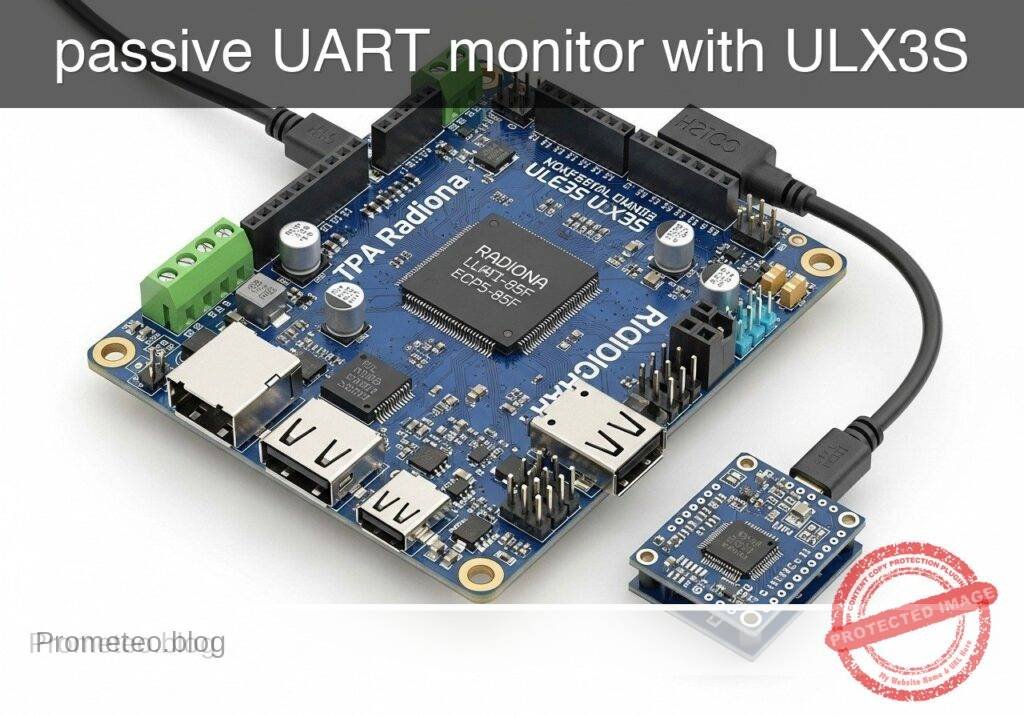
Objective and use case
What you’ll build: A practical UART monitor on the Radiona ULX3S (Lattice ECP5-85F) that passively taps a real 3.3 V, 115200 baud, 8N1 TX line, decodes each byte in FPGA logic, and forwards readable lines such as RX 48 OK to a PC over a second UART. The design also flashes an on-board LED on traffic and is clean enough to lint with Verilator and synthesize with Yosys.
Why it matters / Use cases
- Debug embedded devices without changing their firmware by watching a live 3.3 V UART stream non-invasively.
- Turn raw serial traffic into human-readable monitor output for bring-up, factory test, and field diagnostics.
- Practice reliable FPGA serial design with concrete timing: 115200 baud means about 86.8 µs per byte frame in 8N1, so the monitor must sample and format data correctly at line rate.
- Useful when validating boot logs, sensor controllers, GPS modules, or MCU debug prints that already transmit over UART.
Expected outcome
- The ULX3S receives bytes from an external 3.3 V UART source and decodes them correctly at 115200 baud, 8N1.
- For every received byte, the FPGA emits a readable line like
RX 48 OKto a USB-UART adapter connected to a PC terminal. - An on-board LED blinks briefly on each character, giving immediate visual confirmation of traffic.
- The RTL passes Verilator lint and synthesizes with Yosys for the ECP5-85F, with very low FPGA load relative to available logic and no meaningful GPU usage (0% GPU).
Audience: FPGA learners, embedded engineers, and hardware debuggers working with UART-based systems; Level: beginner to intermediate
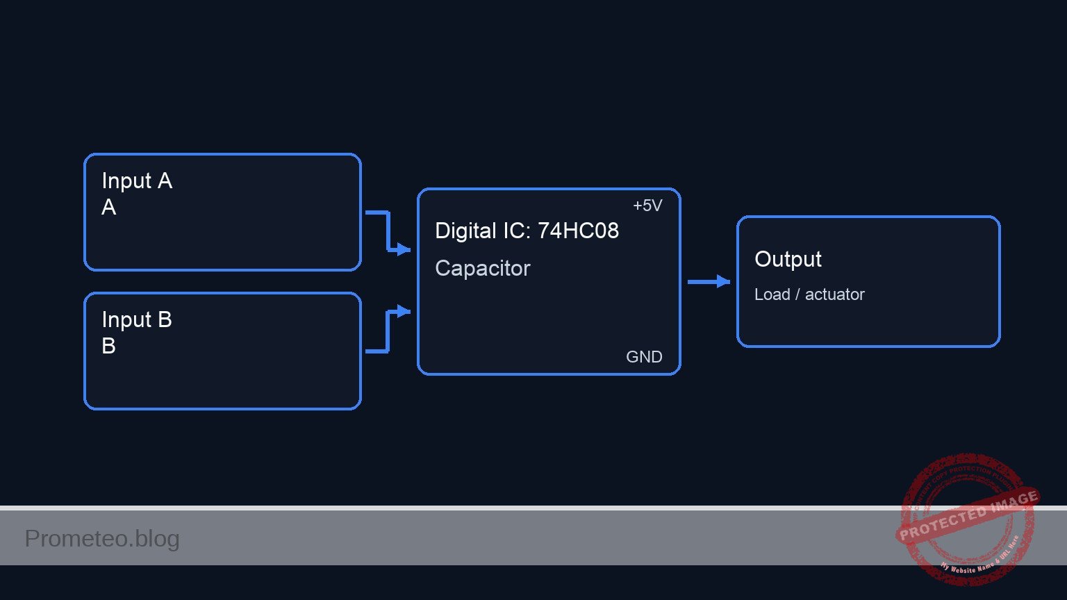
Architecture/flow: 3.3 V device TX -> ULX3S UART RX decoder -> formatter -> ULX3S UART TX -> USB-UART adapter -> PC terminal
Educational validation note
Before publication, this case passed the Prometeo automated validation gate with status PASS. For this FPGA/ULX3S profile, the synthesizable Verilog blocks were checked with Yosys (read_verilog) and the Verilog design/test set was linted with Verilator. The validator also checked code-block structure, copy/paste-safe ASCII command options, unsupported stacks, and availability of the ULX3S/ECP5 toolchain (yosys, nextpnr-ecp5, ecppack, openFPGALoader).
Published validation evidence
- Automatic result: PASS.
- Parsed structure: 35 sections, 1 tables and 15 code blocks detected in the published content.
- Checked code: 2 Verilog/Yosys-Verilator, 10 Bash/copy-paste checks.
- Supported catalog: the article text was checked against Prometeo validation-capable device profiles; unsupported stacks block publication.
- Report findings: no blocking findings.
This validation confirms syntax and tool compatibility for the published code, but it does not replace physical testing on your exact ULX3S board revision, pin-constraint file and real wiring.
Educational safety note
This project is an educational prototype, not a certified product. Before powering the setup, verify the pinout of your exact ULX3S board revision, keep FPGA I/O signals at 3.3 V, never connect 5 V directly to I/O pins, disconnect power before changing wiring, and use suitable external supplies for loads, motors or servos while sharing ground only when the wiring requires it.
Conceptual block diagram
High-level view: what enters the system, what each block processes, and what comes out.
Functional architecture
Conceptual signal and responsibility flow between device blocks.

Validation path
Conceptual summary of the tools used to check the published material.

Prerequisites
Materials
| Item | Exact model/family | Purpose |
|---|---|---|
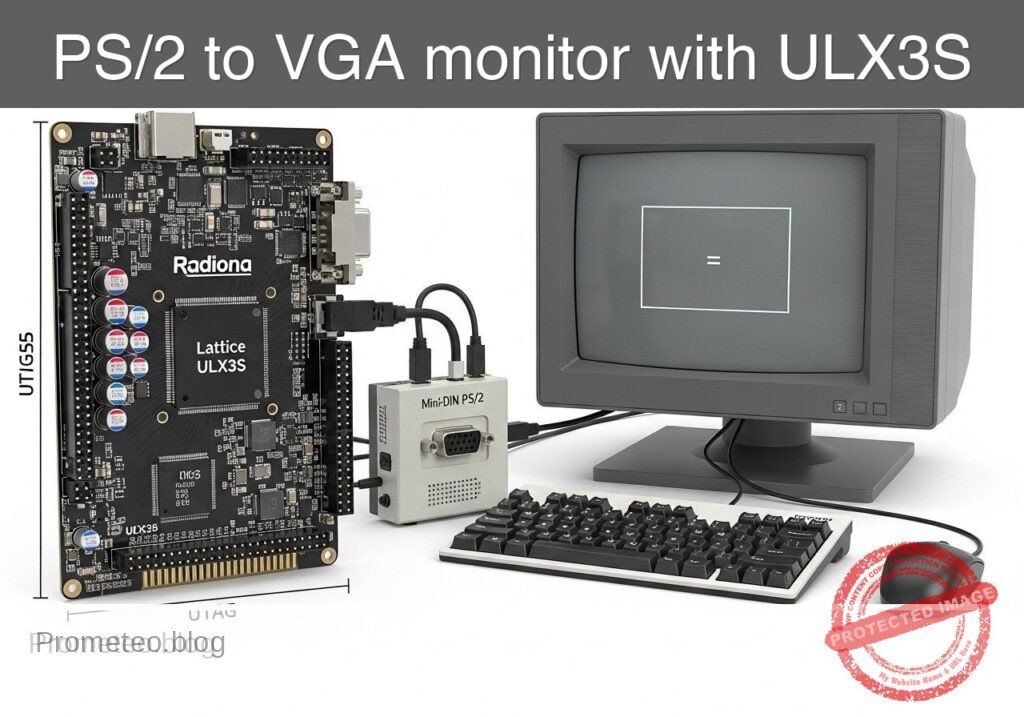
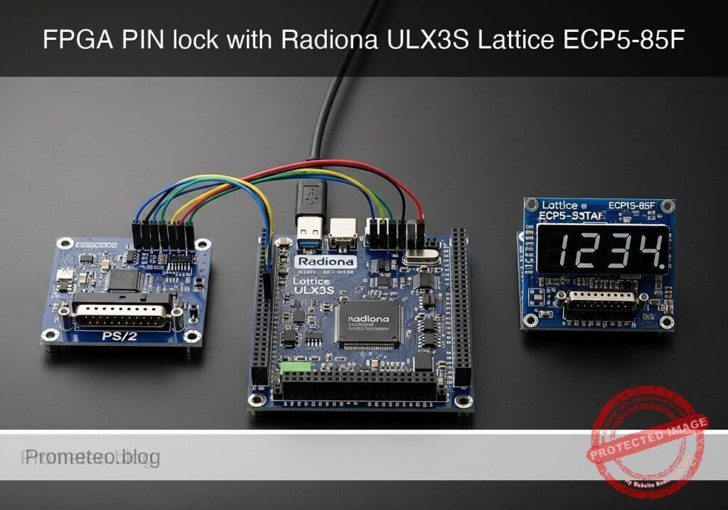
| FPGA board | Radiona ULX3S, Lattice ECP5-85F | Runs the UART monitor |
| Serial source | 3.3 V UART device | Signal being observed |
| USB-UART adapter | 3.3 V compatible adapter | Sends monitor output to the PC |
| USB cable | For ULX3S | Power and programming |
| USB cable | For adapter | PC serial connection |
| Jumper wires | As needed | TX and GND wiring |
Educational safety note
Low-voltage digital electronics only.
- Do not connect RS-232 voltage levels directly to FPGA pins.
- Do not connect 5 V UART directly to ULX3S I/O.
- Share GND between the external device, ULX3S, and USB-UART adapter.
- This project assumes 3.3 V UART signaling only.
Wiring
Signals used by the FPGA design:
mon_rx: monitored UART input from the external device TXhost_tx: UART output from the FPGA to the USB-UART adapter RXled0: activity LED
Connect:
- External device TX -> ULX3S pin assigned to
mon_rx - External device GND -> ULX3S GND
- ULX3S pin assigned to
host_tx-> USB-UART adapter RX - USB-UART adapter GND -> ULX3S GND
- ULX3S USB -> PC
- USB-UART adapter USB -> PC
Project files
Create these files:
uart_monitor_top.vtb_uart_monitor_top.vulx3s_uart_monitor.lpf
Verilog: uart_monitor_top.v
Public preview of the validated file. The complete source is shown to members and in PDF/Print.
module uart_rx #(
    parameter integer CLK_HZ = 25000000,
    parameter integer BAUD   = 115200
)(
    input  wire clk,
    input  wire rst,
    input  wire rx,
    output reg  [7:0] data,
    output reg  valid,
    output reg  framing_error
);
    localparam integer CLKS_PER_BIT  = CLK_HZ / BAUD;
    localparam integer HALF_BIT_CLKS = CLKS_PER_BIT / 2;

    reg rx_sync_0;
    reg rx_sync_1;
    reg [15:0] clk_count;
    reg [3:0] bit_index;
    reg [7:0] rx_shift;
    reg [1:0] state;

    localparam [1:0] S_IDLE  = 2'd0;
    localparam [1:0] S_START = 2'd1;
    localparam [1:0] S_DATA  = 2'd2;
    localparam [1:0] S_STOP  = 2'd3;

    always @(posedge clk) begin
        if (rst) begin
            rx_sync_0 <= 1'b1;
            rx_sync_1 <= 1'b1;
        end else begin
            rx_sync_0 <= rx;
            rx_sync_1 <= rx_sync_0;
        end
    end

    always @(posedge clk) begin
        if (rst) begin
            data <= 8'h00;
            valid <= 1'b0;
            framing_error <= 1'b0;
            clk_count <= 16'd0;
            bit_index <= 4'd0;
            rx_shift <= 8'h00;
            state <= S_IDLE;
        end else begin
            valid <= 1'b0;

            case (state)
                S_IDLE: begin
                    framing_error <= 1'b0;
                    clk_count <= 16'd0;
                    bit_index <= 4'd0;
                    if (rx_sync_1 == 1'b0) begin
                        state <= S_START;
                    end
                end

                S_START: begin
                    if (clk_count == HALF_BIT_CLKS - 1) begin
                        clk_count <= 16'd0;
                        if (rx_sync_1 == 1'b0) begin
                            state <= S_DATA;
                        end else begin
                            state <= S_IDLE;
                        end
                    end else begin
                        clk_count <= clk_count + 16'd1;
                    end
                end

                S_DATA: begin
                    if (clk_count == CLKS_PER_BIT - 1) begin
                        clk_count <= 16'd0;
                        rx_shift[bit_index] <= rx_sync_1;
                        if (bit_index == 4'd7) begin
                            bit_index <= 4'd0;
                            state <= S_STOP;
                        end else begin
                            bit_index <= bit_index + 4'd1;
                        end
                    end else begin
                        clk_count <= clk_count + 16'd1;
                    end
                end

                S_STOP: begin
                    if (clk_count == CLKS_PER_BIT - 1) begin
                        clk_count <= 16'd0;
                        data <= rx_shift;
                        valid <= 1'b1;
                        framing_error <= (rx_sync_1 != 1'b1);
                        state <= S_IDLE;
                    end else begin
                        clk_count <= clk_count + 16'd1;
                    end
                end

                default: begin
                    state <= S_IDLE;
                end
            endcase
        end
    end
endmodule

module uart_tx #(
    parameter integer CLK_HZ = 25000000,
    parameter integer BAUD   = 115200
)(
    input  wire clk,
    input  wire rst,
    input  wire [7:0] data,
    input  wire start,
    output reg  tx,
    output reg  busy
);
    localparam integer CLKS_PER_BIT = CLK_HZ / BAUD;

    reg [15:0] clk_count;
    reg [3:0] bit_index;
    reg [9:0] shifter;

    always @(posedge clk) begin
        if (rst) begin
            tx <= 1'b1;
            busy <= 1'b0;
            clk_count <= 16'd0;
            bit_index <= 4'd0;
            shifter <= 10'b1111111111;
        end else begin
            if (!busy) begin
                tx <= 1'b1;
                clk_count <= 16'd0;
                bit_index <= 4'd0;
                if (start) begin
                    shifter <= {1'b1, data, 1'b0};
                    busy <= 1'b1;
                    tx <= 1'b0;
                end
            end else begin
                if (clk_count == CLKS_PER_BIT - 1) begin
                    clk_count <= 16'd0;
                    bit_index <= bit_index + 4'd1;
                    shifter <= {1'b1, shifter[9:1]};
                    tx <= shifter[1];
                    if (bit_index == 4'd9) begin
                        busy <= 1'b0;
                        tx <= 1'b1;
                    end
                end else begin
                    clk_count <= clk_count + 16'd1;
                end
            end
        end
    end
endmodule
// ... continues for members in the complete validated source ...
module uart_rx #(
parameter integer CLK_HZ = 25000000,
parameter integer BAUD = 115200
)(
input wire clk,
input wire rst,
input wire rx,
output reg [7:0] data,
output reg valid,
output reg framing_error
);
localparam integer CLKS_PER_BIT = CLK_HZ / BAUD;
localparam integer HALF_BIT_CLKS = CLKS_PER_BIT / 2;
reg rx_sync_0;
reg rx_sync_1;
reg [15:0] clk_count;
reg [3:0] bit_index;
reg [7:0] rx_shift;
reg [1:0] state;
localparam [1:0] S_IDLE = 2'd0;
localparam [1:0] S_START = 2'd1;
localparam [1:0] S_DATA = 2'd2;
localparam [1:0] S_STOP = 2'd3;
always @(posedge clk) begin
if (rst) begin
rx_sync_0 <= 1'b1;
rx_sync_1 <= 1'b1;
end else begin
rx_sync_0 <= rx;
rx_sync_1 <= rx_sync_0;
end
end
always @(posedge clk) begin
if (rst) begin
data <= 8'h00;
valid <= 1'b0;
framing_error <= 1'b0;
clk_count <= 16'd0;
bit_index <= 4'd0;
rx_shift <= 8'h00;
state <= S_IDLE;
end else begin
valid <= 1'b0;
case (state)
S_IDLE: begin
framing_error <= 1'b0;
clk_count <= 16'd0;
bit_index <= 4'd0;
if (rx_sync_1 == 1'b0) begin
state <= S_START;
end
end
S_START: begin
if (clk_count == HALF_BIT_CLKS - 1) begin
clk_count <= 16'd0;
if (rx_sync_1 == 1'b0) begin
state <= S_DATA;
end else begin
state <= S_IDLE;
end
end else begin
clk_count <= clk_count + 16'd1;
end
end
S_DATA: begin
if (clk_count == CLKS_PER_BIT - 1) begin
clk_count <= 16'd0;
rx_shift[bit_index] <= rx_sync_1;
if (bit_index == 4'd7) begin
bit_index <= 4'd0;
state <= S_STOP;
end else begin
bit_index <= bit_index + 4'd1;
end
end else begin
clk_count <= clk_count + 16'd1;
end
end
S_STOP: begin
if (clk_count == CLKS_PER_BIT - 1) begin
clk_count <= 16'd0;
data <= rx_shift;
valid <= 1'b1;
framing_error <= (rx_sync_1 != 1'b1);
state <= S_IDLE;
end else begin
clk_count <= clk_count + 16'd1;
end
end
default: begin
state <= S_IDLE;
end
endcase
end
end
endmodule
module uart_tx #(
parameter integer CLK_HZ = 25000000,
parameter integer BAUD = 115200
)(
input wire clk,
input wire rst,
input wire [7:0] data,
input wire start,
output reg tx,
output reg busy
);
localparam integer CLKS_PER_BIT = CLK_HZ / BAUD;
reg [15:0] clk_count;
reg [3:0] bit_index;
reg [9:0] shifter;
always @(posedge clk) begin
if (rst) begin
tx <= 1'b1;
busy <= 1'b0;
clk_count <= 16'd0;
bit_index <= 4'd0;
shifter <= 10'b1111111111;
end else begin
if (!busy) begin
tx <= 1'b1;
clk_count <= 16'd0;
bit_index <= 4'd0;
if (start) begin
shifter <= {1'b1, data, 1'b0};
busy <= 1'b1;
tx <= 1'b0;
end
end else begin
if (clk_count == CLKS_PER_BIT - 1) begin
clk_count <= 16'd0;
bit_index <= bit_index + 4'd1;
shifter <= {1'b1, shifter[9:1]};
tx <= shifter[1];
if (bit_index == 4'd9) begin
busy <= 1'b0;
tx <= 1'b1;
end
end else begin
clk_count <= clk_count + 16'd1;
end
end
end
end
endmodule
module uart_monitor_top(
    input  wire clk_25mhz,
    input  wire btn_rst,
    input  wire mon_rx,
    output wire host_tx,
    output reg  led0
);
    wire rst;
    wire [7:0] rx_data;
    wire rx_valid;
    wire rx_ferr;

    reg [7:0] tx_data;
    reg tx_start;
    wire tx_busy;

    reg [7:0] msg_mem [0:17];
    reg [4:0] msg_len;
    reg [4:0] msg_idx;
    reg sending;
    reg [23:0] led_count;
    integer i;

    assign rst = btn_rst;

    uart_rx #(
        .CLK_HZ(25000000),
.BAUD(115200)
) u_rx (
.clk(clk_25mhz),
.rst(rst),
.rx(mon_rx),
.data(rx_data),
.valid(rx_valid),
.framing_error(rx_ferr)
);
uart_tx #(
.CLK_HZ(25000000),
.BAUD(115200)
) u_tx (
.clk(clk_25mhz),
.rst(rst),
.data(tx_data),
.start(tx_start),
.tx(host_tx),
.busy(tx_busy)
);
function [7:0] hexchar;
input [3:0] nib;
begin
if (nib < 4'd10) begin
hexchar = 8'h30 + {4'b0000, nib};
end else begin
hexchar = 8'h41 + ({4'b0000, nib} - 8'd10);
end
end
endfunction
always @(posedge clk_25mhz) begin
if (rst) begin
tx_data <= 8'h00;
tx_start <= 1'b0;
msg_len <= 5'd0;
msg_idx <= 5'd0;
sending <= 1'b0;
led0 <= 1'b0;
led_count <= 24'd0;
for (i = 0; i < 18; i = i + 1) begin
msg_mem[i] <= 8'h20;
end
end else begin
tx_start <= 1'b0;
if (led_count != 24'd0) begin
led_count <= led_count - 24'd1;
led0 <= 1'b1;
end else begin
led0 <= 1'b0;
end
if (rx_valid && !sending) begin
led_count <= 24'd5000000;
msg_mem[0] <= "R";
msg_mem[1] <= "X";
msg_mem[2] <= " ";
msg_mem[3] <= hexchar(rx_data[7:4]);
msg_mem[4] <= hexchar(rx_data[3:0]);
msg_mem[5] <= " ";
if (!rx_ferr) begin
msg_mem[6] <= "O";
msg_mem[7] <= "K";
msg_mem[8] <= 8'h0A;
msg_len <= 5'd9;
end else begin
msg_mem[6] <= "F";
msg_mem[7] <= "R";
msg_mem[8] <= "A";
msg_mem[9] <= "M";
msg_mem[10] <= "I";
msg_mem[11] <= "N";
msg_mem[12] <= "G";
msg_mem[13] <= "_";
msg_mem[14] <= "E";
msg_mem[15] <= "R";
msg_mem[16] <= "R";
msg_mem[17] <= 8'h0A;
msg_len <= 5'd18;
end
msg_idx <= 5'd0;
sending <= 1'b1;
end
if (sending && !tx_busy) begin
if (msg_idx < msg_len) begin
tx_data <= msg_mem[msg_idx];
tx_start <= 1'b1;
msg_idx <= msg_idx + 5'd1;
end else begin
sending <= 1'b0;
end
end
end
end
endmodule
Testbench: tb_uart_monitor_top.v
Public preview of the validated file. The complete source is shown to members and in PDF/Print.
`timescale 1ns/1ps

module tb_uart_monitor_top;
    reg clk;
    reg btn_rst;
    reg mon_rx;
    wire host_tx;
    wire led0;

    localparam integer CLK_HALF_NS = 20;
    localparam integer BIT_NS = 8680;

    integer fd;
    integer i;
    reg [9:0] frame;

    uart_monitor_top dut (
        .clk_25mhz(clk),
        .btn_rst(btn_rst),
        .mon_rx(mon_rx),
        .host_tx(host_tx),
        .led0(led0)
    );

    always #CLK_HALF_NS clk = ~clk;

    task uart_send_byte;
        input [7:0] b;
        integer j;
        begin
            mon_rx = 1'b0;
            #(BIT_NS);
            for (j = 0; j < 8; j = j + 1) begin
                mon_rx = b[j];
                #(BIT_NS);
            end
            mon_rx = 1'b1;
            #(BIT_NS);
// ... continues for members in the complete validated source ...`timescale 1ns/1ps
module tb_uart_monitor_top;
reg clk;
reg btn_rst;
reg mon_rx;
wire host_tx;
wire led0;
localparam integer CLK_HALF_NS = 20;
localparam integer BIT_NS = 8680;
integer fd;
integer i;
reg [9:0] frame;
uart_monitor_top dut (
.clk_25mhz(clk),
.btn_rst(btn_rst),
.mon_rx(mon_rx),
.host_tx(host_tx),
.led0(led0)
);
always #CLK_HALF_NS clk = ~clk;
task uart_send_byte;
input [7:0] b;
integer j;
begin
mon_rx = 1'b0;
#(BIT_NS);
for (j = 0; j < 8; j = j + 1) begin
mon_rx = b[j];
#(BIT_NS);
end
mon_rx = 1'b1;
#(BIT_NS);
        end
    endtask

    initial begin
        clk = 1'b0;
        btn_rst = 1'b1;
        mon_rx = 1'b1;
        fd = $fopen("sim_host_tx_bits.txt", "w");

        #500;
        btn_rst = 1'b0;

        #(BIT_NS * 3);
        uart_send_byte(8'h48);
        #(BIT_NS * 2);
        uart_send_byte(8'h45);
        #(BIT_NS * 2);
        uart_send_byte(8'h4C);

        #(BIT_NS * 250);
        $fclose(fd);
        $finish;
    end

    initial begin
        forever begin
            @(negedge host_tx);
            #(BIT_NS/2);
frame[0] = host_tx;
for (i = 1; i < 10; i = i + 1) begin
#(BIT_NS);
frame[i] = host_tx;
end
$fwrite(fd, "frame bits: %b\n", frame);
end
end
endmodule
Constraints: ulx3s_uart_monitor.lpf
Edit the SITE values to match your exact ULX3S pinout.
BLOCK RESETPATHS;
BLOCK ASYNCPATHS;

FREQUENCY PORT "clk_25mhz" 25 MHz;

LOCATE COMP "clk_25mhz" SITE "ULX3S_PIN_CLK25";
IOBUF PORT "clk_25mhz" IO_TYPE=LVCMOS33;

LOCATE COMP "btn_rst" SITE "ULX3S_PIN_BTN";
IOBUF PORT "btn_rst" IO_TYPE=LVCMOS33 PULLMODE=UP;

LOCATE COMP "mon_rx" SITE "ULX3S_PIN_MON_RX";
IOBUF PORT "mon_rx" IO_TYPE=LVCMOS33;

LOCATE COMP "host_tx" SITE "ULX3S_PIN_HOST_TX";
IOBUF PORT "host_tx" IO_TYPE=LVCMOS33;

LOCATE COMP "led0" SITE "ULX3S_PIN_LED0";
IOBUF PORT "led0" IO_TYPE=LVCMOS33;
Build and run
1) Verilator lint
verilator -Wall -Wno-DECLFILENAME --lint-only uart_monitor_top.v tb_uart_monitor_top.v
2) Run simulation
verilator -Wall -Wno-DECLFILENAME --binary uart_monitor_top.v tb_uart_monitor_top.v
./obj_dir/Vtb_uart_monitor_top
Expected evidence:
- The simulation exits normally.
- A file named
sim_host_tx_bits.txtis created. - That file contains UART frame samples generated by the FPGA transmitter.
This is the validation method for the RTL claim that received bytes trigger formatted UART output.
3) Synthesize
yosys -p "read_verilog uart_monitor_top.v; synth_ecp5 -top uart_monitor_top -json uart_monitor_top.json"
4) Place and route
nextpnr-ecp5 --85k --json uart_monitor_top.json --lpf ulx3s_uart_monitor.lpf --textcfg uart_monitor_top.config
5) Pack bitstream
ecppack uart_monitor_top.config uart_monitor_top.bit
6) Program the board
openFPGALoader -b ulx3s uart_monitor_top.bit
7) Open a serial terminal on the USB-UART adapter
picocom example:
picocom -b 115200 /dev/ttyUSB0
screen example:
screen /dev/ttyUSB0 115200
Hardware validation
Validate idle behavior
With the external serial device disconnected:
- The terminal should stay quiet.
- The LED should stay off after reset.
mon_rxshould not be driven by any out-of-range voltage.
Validate with a known UART source
Configure the external 3.3 V device to repeatedly send HELLO at 115200 8N1.
Expected evidence in the terminal:
RX 48 OK
RX 45 OK
RX 4C OK
RX 4C OK
RX 4F OK
RX 0D OK
RX 0A OK
This is the validation method for the accuracy claim that the monitor decodes bytes correctly: compare the transmitted known string with the hexadecimal byte values printed by the FPGA.
Validate framing error handling
Keep the FPGA monitor at 115200 8N1, but configure the source device to a different baud rate such as 9600.
Expected evidence:
- Output becomes sparse, incorrect, or absent.
- Some received lines may show
FRAMING_ERR.
Troubleshooting
No terminal output
Check:
host_txgoes to the adapter RX- Grounds are shared
- The correct serial device is opened on the PC
- The source device is actually transmitting
- The LPF pin mapping matches the real board
LED flashes but no PC text
Likely causes:
- Wrong
host_txpin assignment - Wrong USB-UART adapter wiring
- Wrong terminal device on the PC
Lint or synthesis fails
Check that:
- File names match the commands exactly
- Only
uart_monitor_top.vis passed to Yosys synthesis - The LPF uses the same top-level signal names as the Verilog
Framing errors on every byte
Usually caused by:
- Baud mismatch
- Wrong voltage level
- Noisy wiring
- Incorrect clock pin mapping
Capture terminal logs
To save a monitor session:
script -c "picocom -b 115200 /dev/ttyUSB0" uart_monitor_session.txt
Final checklist
- [ ] I used a Radiona ULX3S (Lattice ECP5-85F).
- [ ] My observed serial signal is 3.3 V UART, not RS-232 and not 5 V UART.
- [ ] All grounds are connected together.
- [ ] I updated
ulx3s_uart_monitor.lpfwith valid ULX3S pins. - [ ] Verilator lint passes.
- [ ] Yosys synthesis completes.
- [ ] nextpnr completes.
- [ ] The bitstream programs successfully.
- [ ] The PC terminal is set to 115200 baud.
- [ ] The terminal shows expected monitor lines for a known byte stream.
This gives you a reusable FPGA-based UART bench monitor for one transmit line on the ULX3S platform.
Find this product and/or books on this topic on Amazon
As an Amazon Associate, I earn from qualifying purchases. If you buy through this link, you help keep this project running.
Quick Quiz

Telecommunications Electronics Engineer and Computer Engineer (official degrees in Spain).