Level: Medium – Design a circuit with two photodiodes in a differential configuration to detect the direction of the highest intensity light source.
Objective and use case
You will build a directional light-sensing circuit that uses two reverse-biased photodiodes and an operational amplifier acting as a voltage comparator. By measuring the difference in light intensity between the two sensors, the circuit determines which side is receiving more light.
Why this circuit is useful:
* Maximizing solar panel efficiency by keeping them aimed directly at the sun.
* Enabling autonomous robots to seek out light sources for navigation or charging.
* Automating smart home systems, such as blinds or awnings, to react to direct sunlight direction.
Expected outcome:
* A measurable differential voltage representing the light imbalance between the two sensors.
* Reverse currents through each photodiode strictly proportional to the light hitting them.
* A distinct switching threshold on the operational amplifier’s output based on which sensor yields a higher voltage.
* An LED indicator that clearly illuminates when the left sensor receives more light than the right sensor.
Target audience and level: Intermediate electronics students learning about analog comparators, optoelectronics, and differential measurement.
Materials
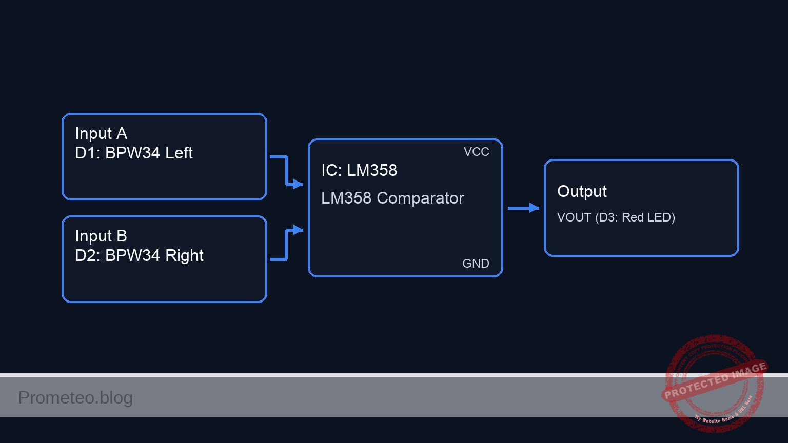
V1: 5 V DC supplyD1: BPW34 photodiode, function: left light sensor (reverse-biased)D2: BPW34 photodiode, function: right light sensor (reverse-biased)R1: 100 kΩ resistor, function: D1 load (current-to-voltage conversion)R2: 100 kΩ resistor, function: D2 load (current-to-voltage conversion)U1: LM358 operational amplifier, function: voltage comparatorR3: 330 Ω resistor, function: LED current limitingD3: red LED, function: left-direction indicator
Wiring guide
V1connects betweenVCCand0.D1connects betweenVCC(cathode) andVL(anode).R1connects betweenVLand0.D2connects betweenVCC(cathode) andVR(anode).R2connects betweenVRand0.U1positive power supply pin connects toVCC.U1negative power supply pin connects to0.U1non-inverting input (IN+) connects toVL.U1inverting input (IN-) connects toVR.U1output connects to nodeVOUT.R3connects betweenVOUTandVLED.D3connects betweenVLED(anode) and0(cathode).
Conceptual block diagram
Schematic
VCC --> [ D1: BPW34 Left ] ---(Node VL)--> [ R1: 100 kΩ ] --> GND
                                  |
                                  +-----(IN+)-----> [             ]
                                                    [ U1: LM358   ]
                                                    [ Comparator  ] --(VOUT)--> [ R3: 330 Ω ] --(VLED)--> [ D3: Red LED ] --> GND
                                  +-----(IN-)-----> [             ]
                                  |
VCC --> [ D2: BPW34 Right ] --(Node VR)--> [ R2: 100 kΩ ] --> GND
Electrical diagram
Measurements and tests
- Reverse Current Verification: Measure the DC voltage drops across
R1andR2. Calculate the reverse photocurrent using Ohm’s Law ($I = V/R$). Ensure the current increases linearly as you move a flashlight closer to the respective photodiode. - Differential Voltage Measurement: Place a multimeter probe on
VLand the other onVR. Shine a light evenly between both sensors; the differential voltage should be near 0 V. Move the light to the left, and the differential voltage should become positive. Move it to the right, and it should become negative. - Switching Threshold Observation: Slowly move a light source from right to left across the sensors. Monitor
VOUTwith a multimeter or oscilloscope. The output should sharply transition from near 0 V (Low) to roughly 3.5 V–4 V (High) precisely whenVL>VR.
SPICE netlist and simulation
Reference SPICE Netlist (ngspice) — excerptFull SPICE netlist (ngspice)
* Optical sensor for a solar tracker
.width out=256

* Power Supply
V1 VCC 0 5V

* Left Light Sensor (D1 and load R1)
* D1 is reverse-biased. I1 simulates the photocurrent generated by light exposure.
D1 VL VCC BPW34
I1 VCC VL PULSE(1u 20u 0 1u 1u 50u 100u)
R1 VL 0 100k

* Right Light Sensor (D2 and load R2)
* D2 is reverse-biased. I2 simulates the photocurrent generated by light exposure.
D2 VR VCC BPW34
I2 VCC VR PULSE(2u 21u 0 1u 1u 100u 200u)
R2 VR 0 100k

* Voltage Comparator (LM358)
XU1 VL VR VCC 0 VOUT LM358
* ... (truncated in public view) ...
Copy this content into a .cir file and run with ngspice.
* Optical sensor for a solar tracker
.width out=256

* Power Supply
V1 VCC 0 5V

* Left Light Sensor (D1 and load R1)
* D1 is reverse-biased. I1 simulates the photocurrent generated by light exposure.
D1 VL VCC BPW34
I1 VCC VL PULSE(1u 20u 0 1u 1u 50u 100u)
R1 VL 0 100k

* Right Light Sensor (D2 and load R2)
* D2 is reverse-biased. I2 simulates the photocurrent generated by light exposure.
D2 VR VCC BPW34
I2 VCC VR PULSE(2u 21u 0 1u 1u 100u 200u)
R2 VR 0 100k

* Voltage Comparator (LM358)
XU1 VL VR VCC 0 VOUT LM358

* Left-Direction Indicator LED
R3 VOUT VLED 330
D3 VLED 0 DLED

* Component Models
.model BPW34 D(IS=5e-10 RS=10 N=1)
.model DLED D(IS=1e-19 N=1.6 RS=10)

* LM358 Operational Amplifier Behavioral Subcircuit (Comparator Mode)
.subckt LM358 in_plus in_minus vcc v_ee out
* Smooth continuous switching to ensure convergence, output swings to VCC - 1.2V
B1 out_ideal 0 V = V(v_ee) + (V(vcc) - V(v_ee) - 1.2) * (0.5 + 0.5 * tanh(1000 * (V(in_plus) - V(in_minus))))
Rout out_ideal out 50
.ends

* Simulation Directives
.op
.tran 1u 400u
.print tran V(VL) V(VR) V(VOUT) V(VLED)
.end
* --- GPT review (BOM/Wiring/SPICE) ---
* circuit_ok=true
* simulation_summary: The simulation shows the circuit acting as a comparator. When the left sensor voltage (VL) is higher than the right sensor voltage (VR), the output (VOUT) goes high (approx 3.5V) and the LED turns on (VLED approx 1.65V). When VR is higher than VL, VOUT goes low (0V) and the LED turns off. This matches the expected behavior of a solar tracker optical sensor.
* bom_vs_spice equivalences ignored:
*   - LM358 operational amplifier is modeled using a behavioral subcircuit (comparator mode).
*   - Photodiodes D1 and D2 are modeled with BPW34 diode models and parallel PULSE current sources (I1, I2) to simulate photocurrent.
*   - Red LED D3 is modeled as a standard diode with a specific model (DLED).
* overall_comment: The SPICE netlist accurately reflects the BOM and wiring guide. The use of current sources to simulate photocurrent in reverse-biased photodiodes is an excellent didactic approach. The behavioral model for the LM358 works well to demonstrate the comparator function. The circuit is fully functional and serves as a great practical example for students.
* --------------------------------------
Simulation Results (Transient Analysis)

Show raw data table (464 rows)
Index   time            v(vl)           v(vr)           v(vout)         v(vled)
0	0.000000e+00	1.000505e-01	2.000505e-01	2.554194e-49	1.941187e-48
1	1.000000e-08	1.190505e-01	2.190505e-01	2.407063e-64	1.829368e-63
2	2.000000e-08	1.380505e-01	2.380505e-01	-2.40706e-64	-1.82937e-63
3	4.000000e-08	1.760505e-01	2.760505e-01	-1.13420e-78	-8.61995e-78
4	8.000000e-08	2.520505e-01	3.520505e-01	4.536814e-79	3.447978e-78
5	1.600000e-07	4.040505e-01	5.040504e-01	3.420381e-93	2.599489e-92
6	3.200000e-07	7.080504e-01	8.080504e-01	-8.55095e-94	-6.49872e-93
7	6.400000e-07	1.316050e+00	1.416050e+00	-8.86422e-108	-6.73681e-107
8	1.000000e-06	2.000050e+00	2.100050e+00	9.065683e-109	6.889919e-108
9	1.064000e-06	2.000050e+00	2.100050e+00	2.491317e-123	1.893401e-122
10	1.192000e-06	2.000050e+00	2.100050e+00	-1.70869e-123	-1.29861e-122
11	1.448000e-06	2.000050e+00	2.100050e+00	-9.52641e-138	-7.24007e-137
12	1.960000e-06	2.000050e+00	2.100050e+00	3.220532e-138	2.447604e-137
13	2.960000e-06	2.000050e+00	2.100050e+00	2.649727e-152	2.013792e-151
14	3.960000e-06	2.000050e+00	2.100050e+00	-3.03502e-153	-2.30661e-152
15	4.960000e-06	2.000050e+00	2.100050e+00	-3.06913e-167	-2.33254e-166
16	5.960000e-06	2.000050e+00	2.100050e+00	2.860189e-168	2.173743e-167
17	6.960000e-06	2.000050e+00	2.100050e+00	3.431423e-182	2.607881e-181
18	7.960000e-06	2.000050e+00	2.100050e+00	-2.69543e-183	-2.04853e-182
19	8.960000e-06	2.000050e+00	2.100050e+00	-3.74179e-197	-2.84376e-196
20	9.960000e-06	2.000050e+00	2.100050e+00	2.540164e-198	1.930525e-197
21	1.096000e-05	2.000050e+00	2.100050e+00	4.005019e-212	3.043815e-211
22	1.196000e-05	2.000050e+00	2.100050e+00	-2.39384e-213	-1.81932e-212
23	1.296000e-05	2.000050e+00	2.100050e+00	-4.22550e-227	-3.21138e-226
... (440 more rows) ...
Common mistakes and how to avoid them
- Forward-biasing the photodiodes: Photodiodes must be reverse-biased to act as light-dependent current sources. If the anode is connected to
VCC, the diode will conduct heavily like a standard diode, bypassing the light-sensing capability. Always ensure the cathode connects to the positive supply. - Using load resistors that are too small: A photodiode’s reverse current is typically in the microampere (µA) range. If
R1andR2are too low (e.g., 1 kΩ), the resulting voltage drop will be too small for the comparator to reliably measure. Stick to high values like 100 kΩ or 1 MΩ. - Lack of optical separation: If both sensors are placed flat next to each other without an optical barrier (a small piece of opaque plastic separating their fields of view), they will receive almost identical light regardless of the angle, preventing the differential circuit from working.
Troubleshooting
- Symptom:
VOUTconstantly fluctuates or the LED flickers continuously.- Cause: The sensors are picking up the 50 Hz / 60 Hz flicker from indoor AC lighting, causing the comparator to oscillate.
- Fix: Add a small capacitor (e.g., 100 nF) in parallel with
R1andR2to act as a low-pass filter, or test the circuit using a DC light source like a flashlight or natural sunlight.
- Symptom: The LED never turns on, even when
D1is flooded with light.- Cause: The LM358 output voltage might not be high enough to overcome the LED’s forward voltage plus the voltage drop of
R3, or the LED is installed backward. - Fix: Verify the LED polarity (anode to
R3, cathode to0). MeasureVOUTto ensure it reaches at least 2 V whenVL>VR.
- Cause: The LM358 output voltage might not be high enough to overcome the LED’s forward voltage plus the voltage drop of
- Symptom: Both
VLandVRremain near 0 V regardless of light.- Cause: The photodiodes might be installed backward (blocking current entirely), or the light intensity is significantly too low for the chosen load resistors.
- Fix: Double-check the photodiode orientation. If correct, increase the value of
R1andR2to 470 kΩ or 1 MΩ to increase sensitivity.
Possible improvements and extensions
- Add Hysteresis: Introduce a high-value feedback resistor (e.g., 1 MΩ) from
VOUTto the non-inverting input (VL). This prevents rapid, noisy switching (chattering) when the light source is perfectly balanced in the center. - Motor Driver Integration: Replace the indicator LED with an H-bridge motor driver (like an L298N or L293D). This allows the circuit to physically drive a DC motor to rotate a platform, creating a fully functional 1-axis physical solar tracker.
More Practical Cases on Prometeo.blog
Find this product and/or books on this topic on Amazon
As an Amazon Associate, I earn from qualifying purchases. If you buy through this link, you help keep this project running.
Quick Quiz

Telecommunications Electronics Engineer and Computer Engineer (official degrees in Spain).