Level: Basic
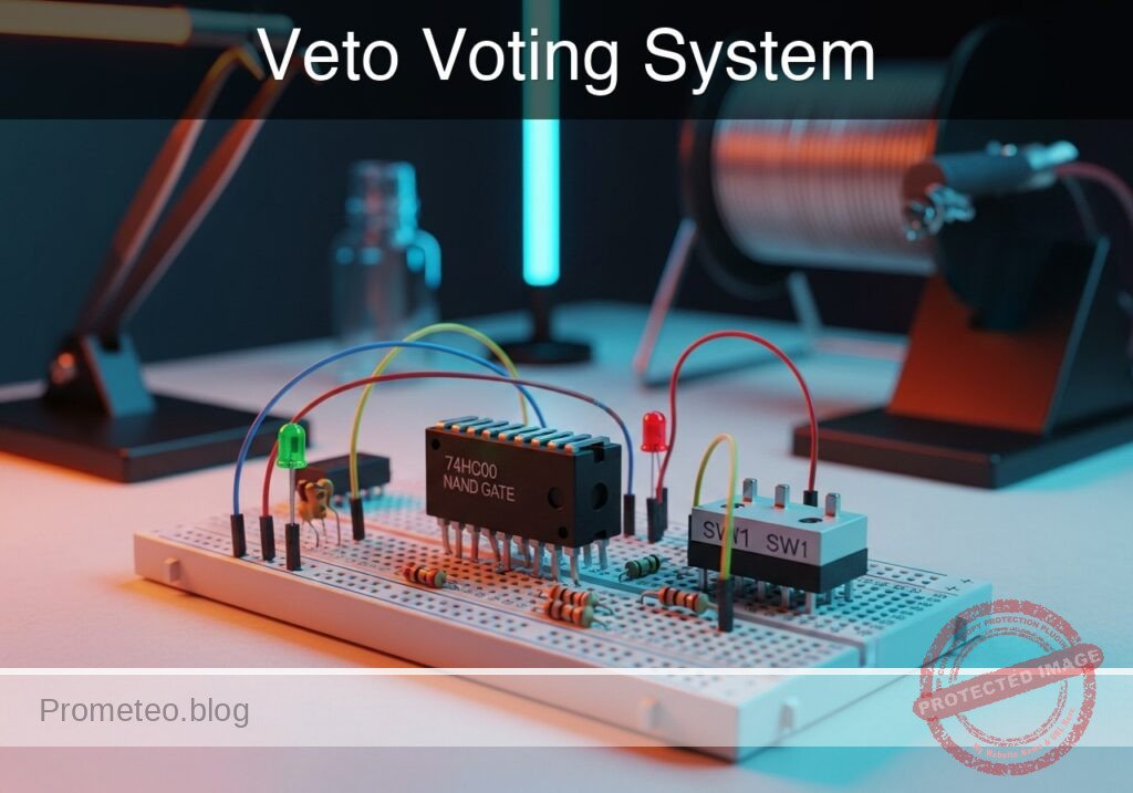
Implement a logic circuit where a proposal passes only if two members vote «Yes» and a third member grants approval (no veto), using a single 74HC00 IC.
Objective and use case
In this practical case, you will build a decision-making circuit using digital logic. The system represents a committee where Member A and Member B must both vote in favor for a motion to pass, but Member C (the Chairperson) holds an «Authorization Key.» If Member C does not activate their switch (Logic Low), the vote is vetoed regardless of A and B.
- Corporate Governance: Models a board where majority support is needed but the CEO has final approval.
- Safety Interlocks: Represents a machine press where two operators must press buttons (A and B), but a Master Enable key (C) must be inserted for the machine to run.
- Security Access: Requires two distinct user keys plus a central server authorization signal.
Expected Outcome:
* Output High (LED ON): Only when Input A is High, Input B is High, AND Input C is High.
* Output Low (LED OFF): Any other combination (e.g., if A or B vote «No», or if C exerts veto by setting their input Low).
* Target Audience: Students and hobbyists learning to construct complex logic functions (3-input AND) using universal NAND gates.
Materials
- U1: 74HC00 (Quad 2-Input NAND Gate)
- SW1: 3-position DIP Switch (or three individual SPST switches), function: Inputs A, B, and C
- R1: 10 kΩ resistor, function: pull-down for Input A
- R2: 10 kΩ resistor, function: pull-down for Input B
- R3: 10 kΩ resistor, function: pull-down for Input C
- R4: 330 Ω resistor, function: LED current limiting
- D1: Red LED, function: Logic Output Indicator
- V1: 5 V DC Power Supply
Pin-out of the IC used
Chip: 74HC00 (Quad 2-input NAND)
This project utilizes all four gates inside the chip to create a 3-input AND function (Y = A · B · C).
| Pin | Name | Logic Function | Connection in this case |
|---|---|---|---|
| 1 | 1 A | Input | Connect to Switch A |
| 2 | 1B | Input | Connect to Switch B |
| 3 | 1Y | Output | Output of Gate 1 (\overlineA · B) |
| 4 | 2 A | Input | Connect to Pin 3 (1Y) |
| 5 | 2B | Input | Connect to Pin 3 (1Y) |
| 6 | 2Y | Output | Output of Gate 2 (Inverted 1Y \to A · B) |
| 7 | GND | Ground | Connect to Power Supply 0 V |
| 8 | 3Y | Output | Output of Gate 3 (\overline(A · B) · C) |
| 9 | 3 A | Input | Connect to Switch C |
| 10 | 3B | Input | Connect to Pin 6 (2Y) |
| 11 | 4Y | Output | Final Output (drives LED) |
| 12 | 4 A | Input | Connect to Pin 8 (3Y) |
| 13 | 4B | Input | Connect to Pin 8 (3Y) |
| 14 | VCC | Power | Connect to +5 V |
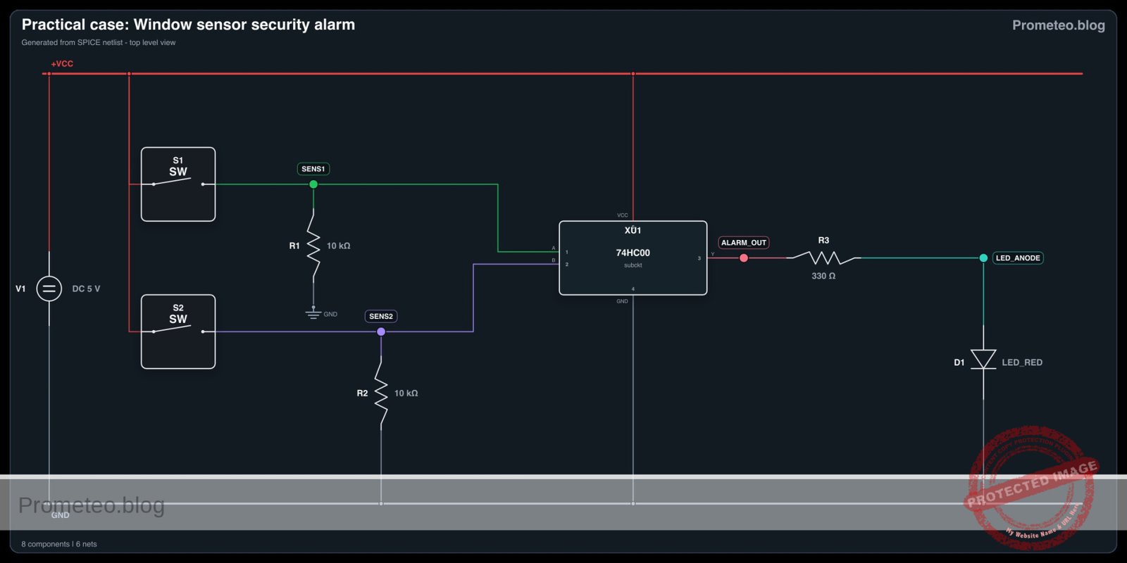
Wiring guide
- VCC: Connect
V1positive terminal,U1pin 14, and the common side ofSW1. - GND: Connect
V1negative terminal,U1pin 7,R1(bottom),R2(bottom),R3(bottom), andD1(cathode). - Input_A: Connect
SW1(Switch 1) toR1(top) andU1pin 1. - Input_B: Connect
SW1(Switch 2) toR2(top) andU1pin 2. - Input_C (Veto): Connect
SW1(Switch 3) toR3(top) andU1pin 9. - Node_NAND1: Connect
U1pin 3 (Output 1) toU1pin 4 andU1pin 5 (Inputs of Gate 2). - Node_AND_AB: Connect
U1pin 6 (Output 2) toU1pin 10 (Input of Gate 3). - Node_NAND_FINAL: Connect
U1pin 8 (Output 3) toU1pin 12 andU1pin 13 (Inputs of Gate 4). - Vout: Connect
U1pin 11 (Final Output) toR4(one side). - LED_Anode: Connect
R4(other side) toD1(anode).
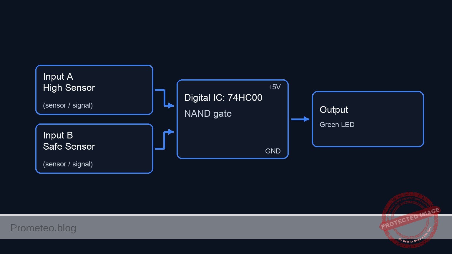
Conceptual block diagram
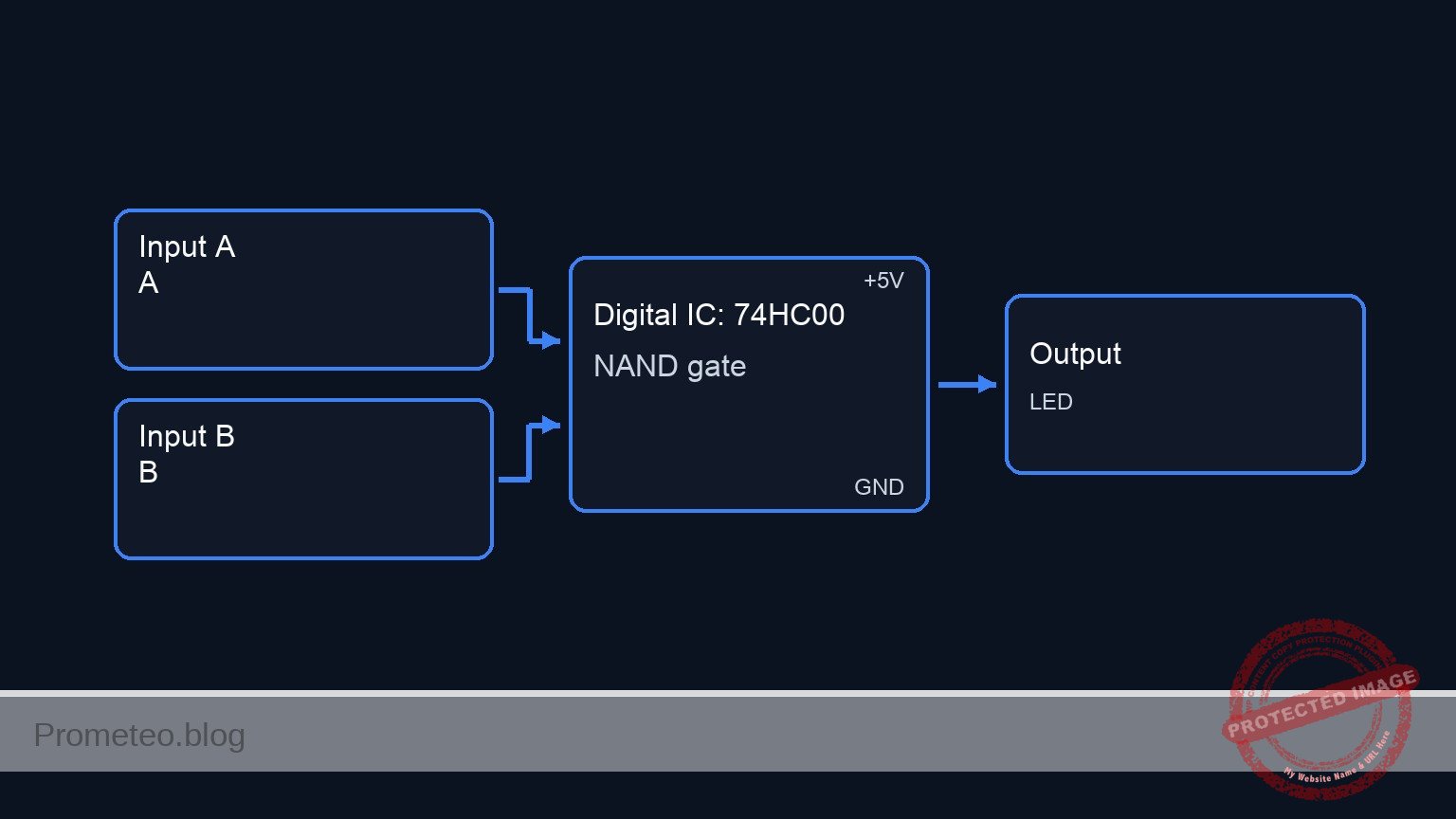
Schematic
Practical Case: Veto Voting System (74HC00 Logic Flow)

INPUTS (Active High)           LOGIC PROCESSING (74HC00 Quad NAND)                               OUTPUT
=======================================================================================================

[ SW A + R1 ] --(Pin 1)-->+
                          |
                    [ U1: Gate 1 ] --(Pin 3)--> [ U1: Gate 2 ] --(Pin 6)---+
                    [ 2-In NAND  ]              [ NAND as NOT]             |
                          |                     (Pins 4+5)                 |
[ SW B + R2 ] --(Pin 2)-->+                                                |
                                                                           |
                                                                           v
                                                                     [ U1: Gate 3 ] --(Pin 8)--> [ U1: Gate 4 ] --(Pin 11)--> [ R4: 330R ] --> [ D1: LED ] --> GND
                                                                     [ 2-In NAND  ]              [ NAND as NOT]
                                                                     (Pin 10)      \             (Pins 12+13)
                                                                                    \
[ SW C + R3 ] -------------------------------------------------------(Pin 9)---------+
(Veto/Enable)

=======================================================================================================
Logic Summary:
1. Gate 1 & 2 form an AND gate for Inputs A & B.
2. Gate 3 & 4 form an AND gate for (Result of A/B) & Input C.
3. Final Function: LED turns ON only if A AND B AND C are all High.
Electrical diagram

Truth table
The circuit implements the logic function Y = A · B · C.
* A/B: Voters
* C: Chairman/Authorization (0 = Veto/Block, 1 = Allow)
| Input A (Voter 1) | Input B (Voter 2) | Input C (Authorization) | Output Y (LED) | Result |
|---|---|---|---|---|
| 0 | 0 | 0 | 0 | Fail |
| 0 | 1 | 1 | 0 | Fail (Lack of votes) |
| 1 | 0 | 1 | 0 | Fail (Lack of votes) |
| 1 | 1 | 0 | 0 | VETOED |
| 1 | 1 | 1 | 1 | Approved |
Measurements and tests
- Supply Check: Before inserting the IC, verify 5 V between VCC and GND lines on your breadboard.
- Default State: Ensure all switches are OFF. Power on. LED should be OFF.
- Veto Test: Turn Switch A and Switch B ON (High). Keep Switch C OFF (Low).
- Observation: LED must remain OFF. This confirms the Veto is active.
- Approval Test: With A and B still ON, turn Switch C ON.
- Observation: LED should light up (Logic High, approx 3.5 V – 4.5 V).
- Single Vote Test: Turn Switch A OFF while B and C are ON.
- Observation: LED should turn OFF.
SPICE netlist and simulation
Reference SPICE Netlist (ngspice) — excerptFull SPICE netlist (ngspice)
* Practical case: Veto Voting System
.width out=256

* ==============================================================================
* Components and Models
* ==============================================================================

* LED Model
.model DLED D(IS=1e-22 RS=10 N=1.5 CJO=10p)

* 74HC00 Quad 2-Input NAND Gate Subcircuit
* Pins: 1=1A, 2=1B, 3=1Y, 4=2A, 5=2B, 6=2Y, 7=GND, 8=3Y, 9=3A, 10=3B, 11=4Y, 12=4A, 13=4B, 14=VCC
.subckt 74HC00 1 2 3 4 5 6 7 8 9 10 11 12 13 14
* Logic Threshold (2.5V) and Gain (20)
.param Vth=2.5
.param K=20
* Gate 1: Inputs 1,2 -> Output 3
B1 3 7 V = V(14,7) * (1 - (1/(1+exp(-K*(V(1,7)-Vth)))) * (1/(1+exp(-K*(V(2,7)-Vth)))))
* Gate 2: Inputs 4,5 -> Output 6
B2 6 7 V = V(14,7) * (1 - (1/(1+exp(-K*(V(4,7)-Vth)))) * (1/(1+exp(-K*(V(5,7)-Vth)))))
* ... (truncated in public view) ...
Copy this content into a .cir file and run with ngspice.
* Practical case: Veto Voting System
.width out=256

* ==============================================================================
* Components and Models
* ==============================================================================

* LED Model
.model DLED D(IS=1e-22 RS=10 N=1.5 CJO=10p)

* 74HC00 Quad 2-Input NAND Gate Subcircuit
* Pins: 1=1A, 2=1B, 3=1Y, 4=2A, 5=2B, 6=2Y, 7=GND, 8=3Y, 9=3A, 10=3B, 11=4Y, 12=4A, 13=4B, 14=VCC
.subckt 74HC00 1 2 3 4 5 6 7 8 9 10 11 12 13 14
* Logic Threshold (2.5V) and Gain (20)
.param Vth=2.5
.param K=20
* Gate 1: Inputs 1,2 -> Output 3
B1 3 7 V = V(14,7) * (1 - (1/(1+exp(-K*(V(1,7)-Vth)))) * (1/(1+exp(-K*(V(2,7)-Vth)))))
* Gate 2: Inputs 4,5 -> Output 6
B2 6 7 V = V(14,7) * (1 - (1/(1+exp(-K*(V(4,7)-Vth)))) * (1/(1+exp(-K*(V(5,7)-Vth)))))
* Gate 3: Inputs 9,10 -> Output 8
B3 8 7 V = V(14,7) * (1 - (1/(1+exp(-K*(V(9,7)-Vth)))) * (1/(1+exp(-K*(V(10,7)-Vth)))))
* Gate 4: Inputs 12,13 -> Output 11
B4 11 7 V = V(14,7) * (1 - (1/(1+exp(-K*(V(12,7)-Vth)))) * (1/(1+exp(-K*(V(13,7)-Vth)))))
.ends 74HC00

* ==============================================================================
* Main Circuit Wiring
* ==============================================================================

* Power Supply (V1)
V1 VCC 0 DC 5

* Inputs (Simulating Switches SW1 positions A, B, C)
* Generating dynamic pulses to test the truth table (000 to 111)
* Input A (LSB, Period 100us)
Va Input_A 0 PULSE(0 5 10u 1u 1u 50u 100u)
* Input B (Period 200us)
Vb Input_B 0 PULSE(0 5 10u 1u 1u 100u 200u)
* Input C (MSB, Period 400us)
Vc Input_C 0 PULSE(0 5 10u 1u 1u 200u 400u)

* Pull-down Resistors (R1, R2, R3)
R1 Input_A 0 10k
R2 Input_B 0 10k
R3 Input_C 0 10k

* Logic IC U1 (74HC00)
* Connectivity based on Wiring Guide:
* Pin 1 (In A) -> Input_A
* Pin 2 (In B) -> Input_B
* Pin 3 (Out 1) -> Node_NAND1
* Pin 4 (In 2A) -> Node_NAND1
* Pin 5 (In 2B) -> Node_NAND1
* Pin 6 (Out 2) -> Node_AND_AB
* Pin 7 (GND)   -> 0
* Pin 8 (Out 3) -> Node_NAND_FINAL
* Pin 9 (In 3A) -> Input_C
* Pin 10 (In 3B)-> Node_AND_AB
* Pin 11 (Out 4)-> Vout
* Pin 12 (In 4A)-> Node_NAND_FINAL
* Pin 13 (In 4B)-> Node_NAND_FINAL
* Pin 14 (VCC)  -> VCC
XU1 Input_A Input_B Node_NAND1 Node_NAND1 Node_NAND1 Node_AND_AB 0 Node_NAND_FINAL Input_C Node_AND_AB Vout Node_NAND_FINAL Node_NAND_FINAL VCC 74HC00

* Output Stage
R4 Vout LED_Anode 330
D1 LED_Anode 0 DLED

* ==============================================================================
* Simulation Commands
* ==============================================================================

.op
.tran 1u 500u

* Print Inputs and Output to check logic (Vout should be High only when A, B, C are High)
.print tran V(Input_A) V(Input_B) V(Input_C) V(Vout)

.end
Simulation Results (Transient Analysis)

Show raw data table (671 rows)
Index   time            v(input_a)      v(input_b)      v(input_c)      v(vout)
0	0.000000e+00	0.000000e+00	0.000000e+00	0.000000e+00	-6.01853e-36
1	1.000000e-08	0.000000e+00	0.000000e+00	0.000000e+00	-6.01853e-36
2	2.000000e-08	0.000000e+00	0.000000e+00	0.000000e+00	-6.01853e-36
3	4.000000e-08	0.000000e+00	0.000000e+00	0.000000e+00	-6.01853e-36
4	8.000000e-08	0.000000e+00	0.000000e+00	0.000000e+00	-6.01853e-36
5	1.600000e-07	0.000000e+00	0.000000e+00	0.000000e+00	-6.01853e-36
6	3.200000e-07	0.000000e+00	0.000000e+00	0.000000e+00	-6.01853e-36
7	6.400000e-07	0.000000e+00	0.000000e+00	0.000000e+00	-6.01853e-36
8	1.280000e-06	0.000000e+00	0.000000e+00	0.000000e+00	-6.01853e-36
9	2.280000e-06	0.000000e+00	0.000000e+00	0.000000e+00	-6.01853e-36
10	3.280000e-06	0.000000e+00	0.000000e+00	0.000000e+00	-6.01853e-36
11	4.280000e-06	0.000000e+00	0.000000e+00	0.000000e+00	-6.01853e-36
12	5.280000e-06	0.000000e+00	0.000000e+00	0.000000e+00	-6.01853e-36
13	6.280000e-06	0.000000e+00	0.000000e+00	0.000000e+00	-6.01853e-36
14	7.280000e-06	0.000000e+00	0.000000e+00	0.000000e+00	-6.01853e-36
15	8.280000e-06	0.000000e+00	0.000000e+00	0.000000e+00	-6.01853e-36
16	9.280000e-06	0.000000e+00	0.000000e+00	0.000000e+00	-6.01853e-36
17	1.000000e-05	0.000000e+00	0.000000e+00	0.000000e+00	-6.01853e-36
18	1.010000e-05	5.000000e-01	5.000000e-01	5.000000e-01	-6.01853e-36
19	1.030000e-05	1.500000e+00	1.500000e+00	1.500000e+00	-6.01853e-36
20	1.048757e-05	2.437858e+00	2.437858e+00	2.437858e+00	-6.01853e-36
21	1.071179e-05	3.558937e+00	3.558937e+00	3.558937e+00	5.000000e+00
22	1.085965e-05	4.298271e+00	4.298271e+00	4.298271e+00	5.000000e+00
23	1.099537e-05	4.976846e+00	4.976846e+00	4.976846e+00	5.000000e+00
... (647 more rows) ...
Common mistakes and how to avoid them
- Floating Inputs: Forgetting the pull-down resistors (R1, R2, R3). Without them, the CMOS inputs of the 74HC00 will float, causing erratic switching or oscillation.
- Confusing Pinout: The 74HC00 pinout is standard, but mixing up Input pins (e.g., 1 A/1B) with Output pins (e.g., 1Y) is common. Double-check the datasheet diagram.
- Misinterpreting «Veto»: In this design, Input C is an «Enable» line (Active High). If you think of Veto as «Switch ON to Block» (Active Low logic), the wiring of Switch C would need to be inverted. Here, Switch C ON means «Authorize».
Troubleshooting
- LED never turns ON: Check that the LED polarity is correct (Anode to resistor, Cathode to GND). Verify U1 is powered (Pin 14 to 5 V, Pin 7 to GND).
- LED stays ON even when switches are OFF: Check if R1, R2, or R3 are missing or disconnected. Ensure you are not using NC (Normally Closed) switches by mistake.
- Circuit works for A and B but C has no effect: Check the wiring on Gate 3 (Pins 8, 9, 10). Ensure pin 9 connects to Switch C and pin 10 connects to the output of the previous stage (Pin 6).
Possible improvements and extensions
- Veto Indicator: Add a second LED (Green) driven by an unused gate (or a transistor) connected to Input C, indicating «Session Open» (Authorization Granted) or «Session Locked» (Veto).
- Majority Vote Modification: Redesign the circuit to allow the proposal to pass if any two of the three members (A, B, C) vote Yes, removing the specific veto power and making all members equal.
More Practical Cases on Prometeo.blog
Find this product and/or books on this topic on Amazon
As an Amazon Associate, I earn from qualifying purchases. If you buy through this link, you help keep this project running.
Quick Quiz

Telecommunications Electronics Engineer and Computer Engineer (official degrees in Spain).