Level: Basic. Control a high-voltage mechanical relay using a small low-power control signal.
Objective and use case
In this practical case, you will build a circuit where a small signal (simulating a microcontroller output like an Arduino) activates an NPN transistor to switch on a 12 V relay.
Why it is useful:
* Microcontroller Protection: Allows delicate 3.3 V or 5 V logic chips to control 12 V or 24 V devices without damage.
* High Current Handling: Transistors can switch relays, which in turn can switch very high currents (AC motors, heaters) that the transistor alone might not handle.
* Automotive Applications: Standard practice for controlling 12 V automotive accessories from an ECU.
* Isolation: While the transistor shares a ground, the relay contacts provide galvanic isolation for the final load.
Expected outcome:
* When the 5 V switch is closed, the transistor saturates (VCE ≈ 0.2 V).
* The relay coil energizes, producing an audible «click.»
* The load LED turns ON.
* The flyback diode protects the transistor from high-voltage spikes when the relay turns OFF.
Target audience and level:
Basic electronics students and hobbyists.
Materials
- V1: 5 V DC supply, function: Logic control voltage source.
- V2: 12 V DC supply, function: Relay coil and load power.
- S1: SPST Toggle Switch, function: Simulates the microcontroller output pin.
- R1: 1 kΩ resistor, function: Base current limiting to ensure saturation.
- Q1: 2N2222 (NPN BJT), function: Low-side switch driver.
- K1: 12 V SPDT Relay, function: Electromechanical switching element.
- D1: 1N4007 Diode, function: Flyback (freewheeling) protection diode.
- R2: 470 Ω resistor, function: Current limiting for the load LED.
- D2: Green LED, function: Visual indicator of the load status (connected to Relay NO contact).
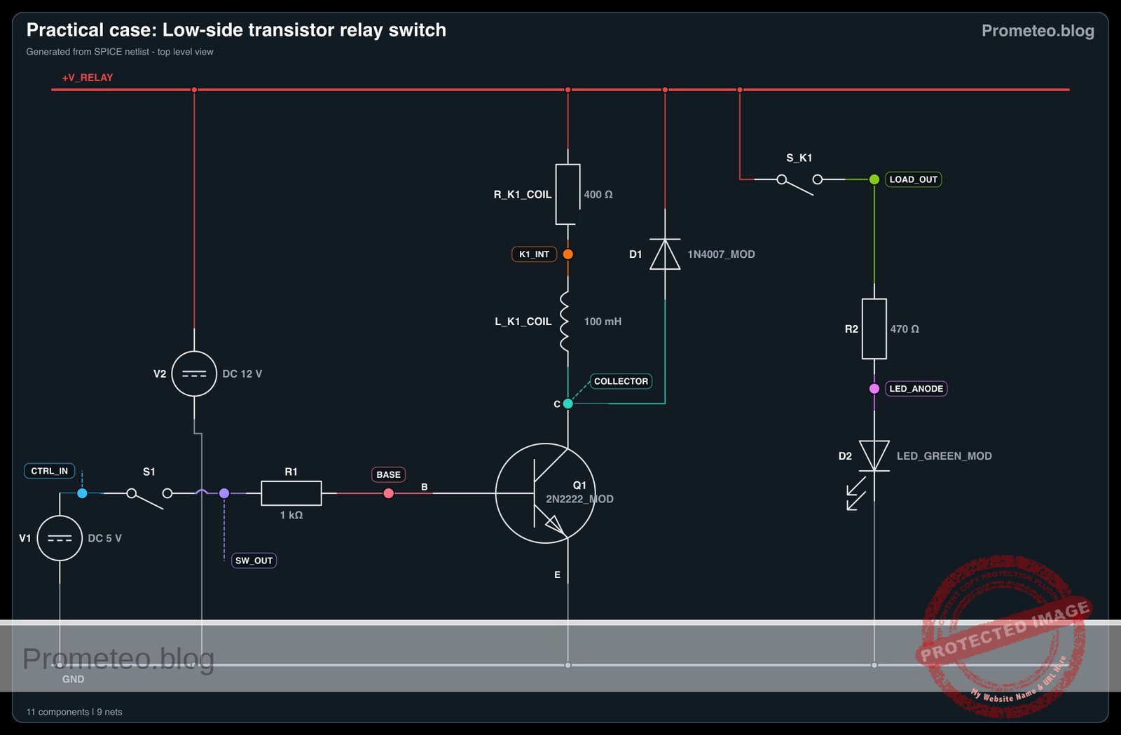
Wiring guide
This guide uses specific node names to define the connections clearly.
* Nodes: GND (Common Ground), CTRL_IN (5 V Logic), V_RELAY (12 V Supply), BASE, COLLECTOR, LOAD_OUT.
- V1: Positive terminal to
CTRL_IN, Negative terminal toGND. - V2: Positive terminal to
V_RELAY, Negative terminal toGND. - S1: Connected between
CTRL_INand input of R1. - R1: Connected between Output of S1 and
BASEof Q1. - Q1:
- Base to
BASE. - Emitter to
GND. - Collector to
COLLECTOR.
- Base to
- K1 (Coil): Connected between
V_RELAYandCOLLECTOR. - D1: Anode to
COLLECTOR, Cathode toV_RELAY(Reverse biased). - K1 (Common Contact): Connected to
V_RELAY. - K1 (Normally Open – NO): Connected to
LOAD_OUT. - R2: Connected between
LOAD_OUTand Anode of D2. - D2: Anode to R2, Cathode to
GND.
Conceptual block diagram
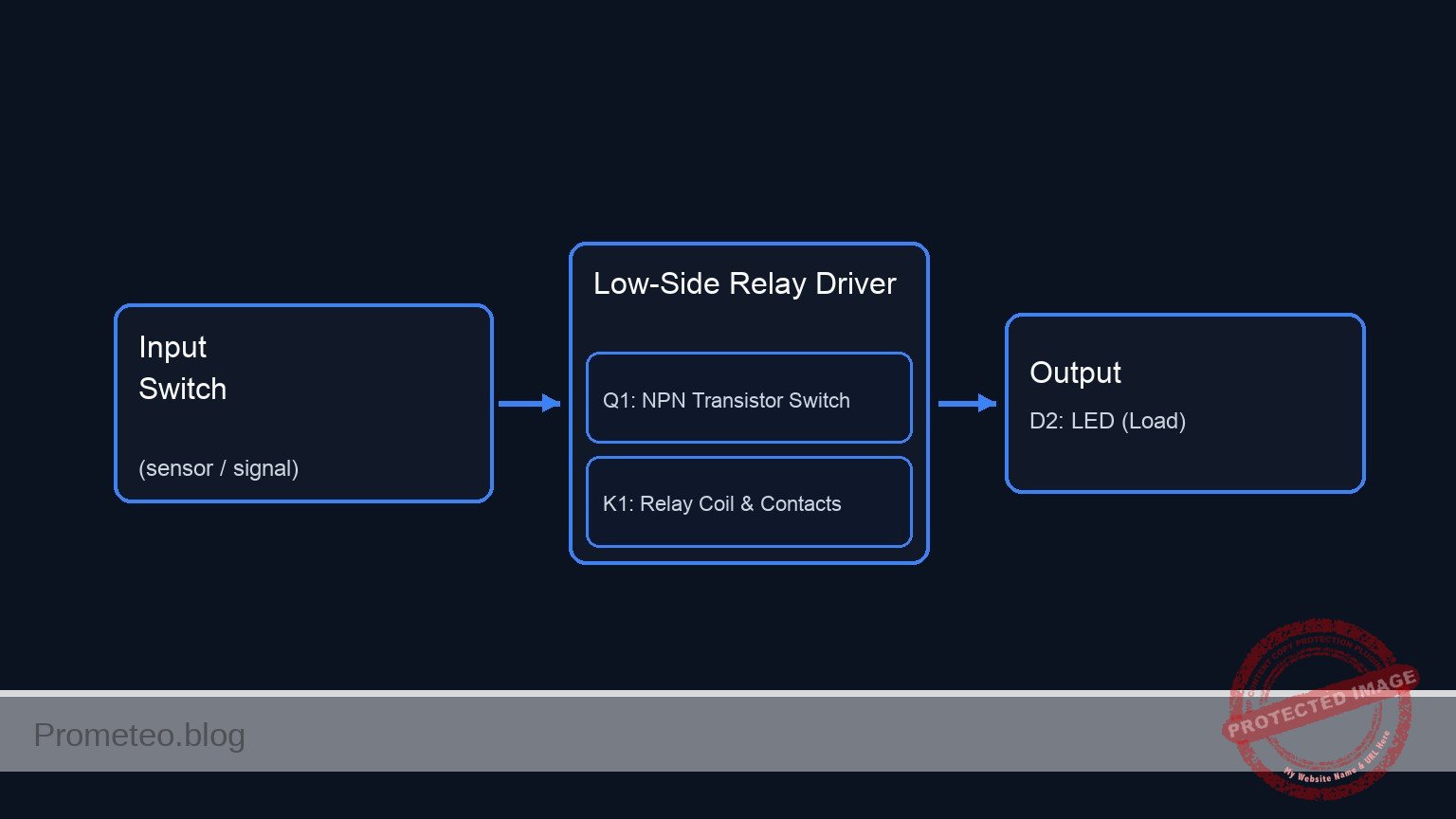
Schematic
Title: Practical case: Low-Side Transistor Relay Switch

1. CONTROL LOOP (Logic Signal)
   Flow: 5 V Logic activates the Transistor Base.

   [ V1: 5 V ] --(Node: CTRL_IN)--> [ S1: Switch ] --> [ R1: 1k ] --(Node: BASE)--> [ Q1: Base ]
                                                                                         |
                                                                                         | (Controls Q1 State)
                                                                                         v

2. RELAY DRIVE LOOP (12 V Power & Coil)
   Flow: Transistor sinks Coil current to Ground; Diode protects against spikes.

                                           (Flyback Protection)
                             .-----[ D1: Cathode <------- Anode ]------.
                             |                                         |
                             v                                         v
   [ V2: 12 V ] --(Node: V_RELAY)--> [ K1: Coil ] --(Node: COLLECTOR)--> [ Q1: Collector ]
                                                                               |
                                                                               | (Current Flow)
                                                                               v
                                                                        [ Q1: Emitter ] --> GND


3. LOAD LOOP (High Power Output)
   Flow: Relay Magnetic Field closes the switch, powering the LED.

          .--------------------------( Magnetic Mechanical Link )--------------------------.
          |                                                                                |
          v                                                                                v
   [ V2: 12 V ] --> [ K1: COM ] --( Switch Closes )--> [ K1: NO ] --(Node: LOAD_OUT)--> [ R2: 470R ] --> [ D2: LED ] --> GND
Electrical diagram
Measurements and tests
Follow these steps to validate the circuit operation using a multimeter:
- OFF State check: Ensure S1 is Open. Measure voltage at
COLLECTORrelative toGND. It should be close to 12 V (floating through the coil). D2 should be OFF. - Activation: Close S1. Listen for the relay click. D2 should turn ON.
- Base-Emitter Voltage (VBE): With S1 closed, measure voltage between
BASEandGND. It should be approx 0.7 V – 0.8 V. - Saturation Verification (VCE): Measure voltage between
COLLECTORandGNDwhile ON. It should be very low (typically < 0.2 V), indicating the transistor is acting like a closed switch. - Coil Voltage: Measure across the relay coil. It should read close to 11.8 V (12 V supply minus the small VCE drop).
SPICE netlist and simulation
Reference SPICE Netlist (ngspice) — excerptFull SPICE netlist (ngspice)
* Practical case: Low-Side Transistor Relay Switch
.width out=256
*
* Description:
* A 5V control signal (simulated via S1) drives a 2N2222 NPN transistor.
* The transistor switches a 12V Relay Coil.
* The Relay contacts switch a 12V load (Green LED).
*
* Nodes defined in Wiring Guide:
* GND, CTRL_IN, V_RELAY, BASE, COLLECTOR, LOAD_OUT

* --- Power Supplies ---
* V1: 5V Logic Supply
V1 CTRL_IN 0 DC 5
* V2: 12V Relay/Load Supply
V2 V_RELAY 0 DC 12

* --- User Switch Simulation (S1) ---
* S1 represents the physical SPST toggle switch.
* We use a voltage-controlled switch model driven by a PULSE source (V_USER)
* ... (truncated in public view) ...
Copy this content into a .cir file and run with ngspice.
* Practical case: Low-Side Transistor Relay Switch
.width out=256
*
* Description:
* A 5V control signal (simulated via S1) drives a 2N2222 NPN transistor.
* The transistor switches a 12V Relay Coil.
* The Relay contacts switch a 12V load (Green LED).
*
* Nodes defined in Wiring Guide:
* GND, CTRL_IN, V_RELAY, BASE, COLLECTOR, LOAD_OUT

* --- Power Supplies ---
* V1: 5V Logic Supply
V1 CTRL_IN 0 DC 5
* V2: 12V Relay/Load Supply
V2 V_RELAY 0 DC 12

* --- User Switch Simulation (S1) ---
* S1 represents the physical SPST toggle switch.
* We use a voltage-controlled switch model driven by a PULSE source (V_USER)
* to simulate the user pressing/releasing the switch.
* Timing: Wait 5ms, ON for 20ms, Period 50ms.
V_USER S1_CTRL 0 PULSE(0 5 5m 10u 10u 20m 50m)

* S1 Instance: Connects CTRL_IN to SW_OUT when S1_CTRL is high.
S1 CTRL_IN SW_OUT S1_CTRL 0 TACTILE_SW

* --- Base Drive ---
* R1: Current limiting for Q1 Base
R1 SW_OUT BASE 1k

* --- Low-Side Driver (Q1) ---
* Q1: NPN 2N2222
* Connections: Collector, Base, Emitter(GND)
Q1 COLLECTOR BASE 0 2N2222_MOD

* --- Relay Coil & Flyback Diode ---
* K1 Coil: Modeled as Inductance (L) + Series Resistance (R).
* Connected between V_RELAY (12V) and COLLECTOR.
* Typical 12V relay coil resistance ~400 Ohms.
R_K1_COIL V_RELAY K1_INT 400
L_K1_COIL K1_INT COLLECTOR 100m

* D1: 1N4007 Flyback Diode (Reverse biased)
* Anode to COLLECTOR, Cathode to V_RELAY
D1 COLLECTOR V_RELAY 1N4007_MOD

* --- Relay Contacts (K1 Switch) ---
* Modeled as a voltage-controlled switch (S_K1).
* Controlled by the voltage across the coil (V_RELAY - COLLECTOR).
* When Q1 is ON, Coil Voltage ~ 12V -> Contacts Close.
* When Q1 is OFF, Coil Voltage ~ 0V -> Contacts Open.
* Connections: Common (V_RELAY) to NO (LOAD_OUT).
S_K1 V_RELAY LOAD_OUT V_RELAY COLLECTOR RELAY_SW_MOD

* --- Load Circuit ---
* R2: Current limiting for LED
R2 LOAD_OUT LED_ANODE 470
* D2: Green LED
D2 LED_ANODE 0 LED_GREEN_MOD

* --- Component Models ---

* Switch Model for S1 (Logic Level Control)
.model TACTILE_SW SW(Vt=2.5 Vh=0.5 Ron=0.01 Roff=100Meg)

* Switch Model for Relay (High Voltage Threshold)
* Vt=8V ensures it pulls in only when coil is energized (approx >8V)
.model RELAY_SW_MOD SW(Vt=8.0 Vh=1.0 Ron=0.05 Roff=100Meg)

* BJT Model 2N2222
.model 2N2222_MOD NPN(IS=1E-14 VAF=100 BF=200 IKF=0.3 XTB=1.5 BR=3 CJC=8E-12 CJE=25E-12 TR=46.91E-9 TF=411.1E-12 ITF=0.6 VTF=1.7 XTF=3 RB=10 RC=1 RE=0.1)

* Diode Model 1N4007
.model 1N4007_MOD D(IS=7n RS=0.034 N=1.8 BV=1000 IBV=5e-8 CJO=10p VJ=0.7 M=0.5 TT=100n)

* LED Model (Green, approx 2.1V Vf)
.model LED_GREEN_MOD D(IS=1e-22 RS=5 N=1.8 CJO=50p VJ=2.2 BV=5 IBV=10u)

* --- Analysis Directives ---
.op
.tran 100u 60m

* Output Printing
* V(SW_OUT): Input signal after switch S1
* V(LOAD_OUT): Output status (Relay NO contact)
* V(BASE): Transistor Base Voltage
* V(COLLECTOR): Transistor Collector Voltage (Relay Coil Low-Side)
.print tran V(SW_OUT) V(LOAD_OUT) V(BASE) V(COLLECTOR) I(L_K1_COIL)

.end
Simulation Results (Transient Analysis)

Show raw data table (722 rows)
Index   time            v(sw_out)       v(load_out)     v(base)         v(collector)    l_k1_coil#branc
0	0.000000e+00	5.331417e-01	1.609847e+00	5.330970e-01	1.199602e+01	9.959371e-06
1	1.000000e-06	5.331417e-01	1.609847e+00	5.330970e-01	1.199602e+01	9.959371e-06
2	2.000000e-06	5.331417e-01	1.609847e+00	5.330970e-01	1.199602e+01	9.959371e-06
3	4.000000e-06	5.331417e-01	1.609847e+00	5.330970e-01	1.199602e+01	9.959371e-06
4	8.000000e-06	5.331417e-01	1.609847e+00	5.330970e-01	1.199602e+01	9.959371e-06
5	1.600000e-05	5.331417e-01	1.609847e+00	5.330970e-01	1.199602e+01	9.959371e-06
6	3.200000e-05	5.331417e-01	1.609847e+00	5.330970e-01	1.199602e+01	9.959371e-06
7	6.400000e-05	5.331417e-01	1.609847e+00	5.330970e-01	1.199602e+01	9.959371e-06
8	1.280000e-04	5.331417e-01	1.609847e+00	5.330970e-01	1.199602e+01	9.959371e-06
9	2.280000e-04	5.331417e-01	1.609847e+00	5.330970e-01	1.199602e+01	9.959371e-06
10	3.280000e-04	5.331417e-01	1.609847e+00	5.330970e-01	1.199602e+01	9.959371e-06
11	4.280000e-04	5.331417e-01	1.609847e+00	5.330970e-01	1.199602e+01	9.959371e-06
12	5.280000e-04	5.331417e-01	1.609847e+00	5.330970e-01	1.199602e+01	9.959371e-06
13	6.280000e-04	5.331417e-01	1.609847e+00	5.330970e-01	1.199602e+01	9.959371e-06
14	7.280000e-04	5.331417e-01	1.609847e+00	5.330970e-01	1.199602e+01	9.959371e-06
15	8.280000e-04	5.331417e-01	1.609847e+00	5.330970e-01	1.199602e+01	9.959371e-06
16	9.280000e-04	5.331417e-01	1.609847e+00	5.330970e-01	1.199602e+01	9.959371e-06
17	1.028000e-03	5.331417e-01	1.609847e+00	5.330970e-01	1.199602e+01	9.959371e-06
18	1.128000e-03	5.331417e-01	1.609847e+00	5.330970e-01	1.199602e+01	9.959371e-06
19	1.228000e-03	5.331417e-01	1.609847e+00	5.330970e-01	1.199602e+01	9.959371e-06
20	1.328000e-03	5.331417e-01	1.609847e+00	5.330970e-01	1.199602e+01	9.959371e-06
21	1.428000e-03	5.331417e-01	1.609847e+00	5.330970e-01	1.199602e+01	9.959371e-06
22	1.528000e-03	5.331417e-01	1.609847e+00	5.330970e-01	1.199602e+01	9.959371e-06
23	1.628000e-03	5.331417e-01	1.609847e+00	5.330970e-01	1.199602e+01	9.959371e-06
... (698 more rows) ...
Reference SPICE netlist (ngspice)
* Practical case: Low-Side Transistor Relay Switch
.width out=256
*
* Description:
* A 5V control signal (simulated via S1) drives a 2N2222 NPN transistor.
* The transistor switches a 12V Relay Coil.
* The Relay contacts switch a 12V load (Green LED).
*
* Nodes defined in Wiring Guide:
* GND, CTRL_IN, V_RELAY, BASE, COLLECTOR, LOAD_OUT

* --- Power Supplies ---
* V1: 5V Logic Supply
V1 CTRL_IN 0 DC 5
* V2: 12V Relay/Load Supply
V2 V_RELAY 0 DC 12

* --- User Switch Simulation (S1) ---
* S1 represents the physical SPST toggle switch.
* We use a voltage-controlled switch model driven by a PULSE source (V_USER)
* to simulate the user pressing/releasing the switch.
* Timing: Wait 5ms, ON for 20ms, Period 50ms.
V_USER S1_CTRL 0 PULSE(0 5 5m 10u 10u 20m 50m)

* S1 Instance: Connects CTRL_IN to SW_OUT when S1_CTRL is high.
S1 CTRL_IN SW_OUT S1_CTRL 0 TACTILE_SW

* --- Base Drive ---
* R1: Current limiting for Q1 Base
R1 SW_OUT BASE 1k

* --- Low-Side Driver (Q1) ---
* Q1: NPN 2N2222
* Connections: Collector, Base, Emitter(GND)
Q1 COLLECTOR BASE 0 2N2222_MOD

* --- Relay Coil & Flyback Diode ---
* K1 Coil: Modeled as Inductance (L) + Series Resistance (R).
* Connected between V_RELAY (12V) and COLLECTOR.
* Typical 12V relay coil resistance ~400 Ohms.
R_K1_COIL V_RELAY K1_INT 400
L_K1_COIL K1_INT COLLECTOR 100m

* D1: 1N4007 Flyback Diode (Reverse biased)
* Anode to COLLECTOR, Cathode to V_RELAY
D1 COLLECTOR V_RELAY 1N4007_MOD

* --- Relay Contacts (K1 Switch) ---
* Modeled as a voltage-controlled switch (S_K1).
* Controlled by the voltage across the coil (V_RELAY - COLLECTOR).
* When Q1 is ON, Coil Voltage ~ 12V -> Contacts Close.
* When Q1 is OFF, Coil Voltage ~ 0V -> Contacts Open.
* Connections: Common (V_RELAY) to NO (LOAD_OUT).
S_K1 V_RELAY LOAD_OUT V_RELAY COLLECTOR RELAY_SW_MOD

* --- Load Circuit ---
* R2: Current limiting for LED
R2 LOAD_OUT LED_ANODE 470
* D2: Green LED
D2 LED_ANODE 0 LED_GREEN_MOD

* --- Component Models ---

* Switch Model for S1 (Logic Level Control)
.model TACTILE_SW SW(Vt=2.5 Vh=0.5 Ron=0.01 Roff=100Meg)

* Switch Model for Relay (High Voltage Threshold)
* Vt=8V ensures it pulls in only when coil is energized (approx >8V)
.model RELAY_SW_MOD SW(Vt=8.0 Vh=1.0 Ron=0.05 Roff=100Meg)

* BJT Model 2N2222
.model 2N2222_MOD NPN(IS=1E-14 VAF=100 BF=200 IKF=0.3 XTB=1.5 BR=3 CJC=8E-12 CJE=25E-12 TR=46.91E-9 TF=411.1E-12 ITF=0.6 VTF=1.7 XTF=3 RB=10 RC=1 RE=0.1)

* Diode Model 1N4007
.model 1N4007_MOD D(IS=7n RS=0.034 N=1.8 BV=1000 IBV=5e-8 CJO=10p VJ=0.7 M=0.5 TT=100n)

* LED Model (Green, approx 2.1V Vf)
.model LED_GREEN_MOD D(IS=1e-22 RS=5 N=1.8 CJO=50p VJ=2.2 BV=5 IBV=10u)

* --- Analysis Directives ---
.op
.tran 100u 60m

* Output Printing
* V(SW_OUT): Input signal after switch S1
* V(LOAD_OUT): Output status (Relay NO contact)
* V(BASE): Transistor Base Voltage
* V(COLLECTOR): Transistor Collector Voltage (Relay Coil Low-Side)
.print tran V(SW_OUT) V(LOAD_OUT) V(BASE) V(COLLECTOR) I(L_K1_COIL)

.end
Simulation Results (Transient Analysis)
Common mistakes and how to avoid them
- Omitting the flyback diode (D1):
- Consequence: The high-voltage spike generated by the relay coil collapsing can destroy the transistor immediately.
- Solution: Always install a diode in parallel with the coil, cathode to positive voltage.
- Using a base resistor (R1) that is too high:
- Consequence: The transistor operates in the active region instead of saturation, causing it to overheat and potentially fail to trigger the relay.
- Solution: Calculate IB to be at least 5× to 10× the required base current for the given collector load.
- Connecting the load to the Emitter (High-side):
- Consequence: The relay will not receive 12 V; it will only receive approx Vbase – 0.7 V (approx 4.3 V), which is insufficient to actuate a 12 V relay.
- Solution: Always use NPN transistors as «Low-side» switches (Load connected to Collector, Emitter to Ground).
Troubleshooting
- Symptom: Relay does not click, LED D2 stays off.
- Cause: S1 is not connecting or R1 is too large.
- Fix: Check continuity on S1 and verify 5 V is reaching R1.
- Symptom: Transistor gets very hot when Relay is ON.
- Cause: Transistor is not fully saturated (Base current too low).
- Fix: Reduce R1 value (e.g., try 470 Ω) to push Q1 into deep saturation.
- Symptom: Circuit worked once, then stopped working permanently.
- Cause: D1 is missing or reversed (causing short circuit) or Q1 is blown.
- Fix: Replace Q1 and ensure D1 is correctly installed (Cathode to +12 V).
- Symptom: D2 turns on, but no «click» is heard.
- Cause: You might be testing with a solid-state indicator instead of a mechanical relay, or the relay coil is damaged.
- Fix: Verify the coil resistance matches the datasheet specifications.
Possible improvements and extensions
- MOSFET Upgrade: Replace the NPN BJT with an N-Channel Logic-Level MOSFET (e.g., IRLZ44N) for higher efficiency and zero gate current draw.
- Optical Isolation: Add an optocoupler (like 4N25) before Q1 to completely electrically isolate the 5 V control side from the 12 V power side, protecting the microcontroller from catastrophic power failures.
More Practical Cases on Prometeo.blog
Find this product and/or books on this topic on Amazon
As an Amazon Associate, I earn from qualifying purchases. If you buy through this link, you help keep this project running.
Quick Quiz

Telecommunications Electronics Engineer and Computer Engineer (official degrees in Spain).