Level: Medium — Design and analyze a circuit that attenuates high frequencies using a capacitor and a resistor to verify the cutoff frequency.
Objective and use case
In this practical case, you will build a passive first-order Low-Pass Filter (LPF) using a resistor and a capacitor connected in series. You will analyze how the capacitor’s reactance changes with frequency, allowing low frequencies to pass while attenuating signals above a calculated cutoff point.
Why it is useful:
* Audio noise reduction: Removes high-frequency hiss or static from audio recordings.
* Subwoofer crossovers: Directs only low-frequency bass notes to the subwoofer driver.
* Signal conditioning: Acts as an anti-aliasing filter before Analog-to-Digital Conversion (ADC) to prevent digital artifacts.
* Power supply smoothing: Filters out high-frequency ripple noise from DC power lines.
Expected outcome:
* Passband: Frequencies below ~1 kHz retain approximately their original amplitude (Vin ≈ Vout).
* Cutoff point: At the calculated cutoff frequency (fc), the output voltage drops to approximately 70.7% of the input voltage (-3 dB).
* Stopband: Frequencies significantly higher than 1 kHz are heavily attenuated.
* Phase shift: Observe a phase lag of -45° at the cutoff frequency.
Target audience and level: Electronics students and audio enthusiasts; Level: Medium.
Materials
- V1: AC Voltage Source (Sine Wave, 5 Vpk, tunable frequency), function: Input audio signal simulation.
- R1: 1.6 kΩ resistor, function: Current limiting and voltage division partner.
- C1: 100 nF capacitor (ceramic or film), function: Frequency-dependent shunt to ground.
- Measurement Tool: Oscilloscope (Dual channel) or Bode Plotter.
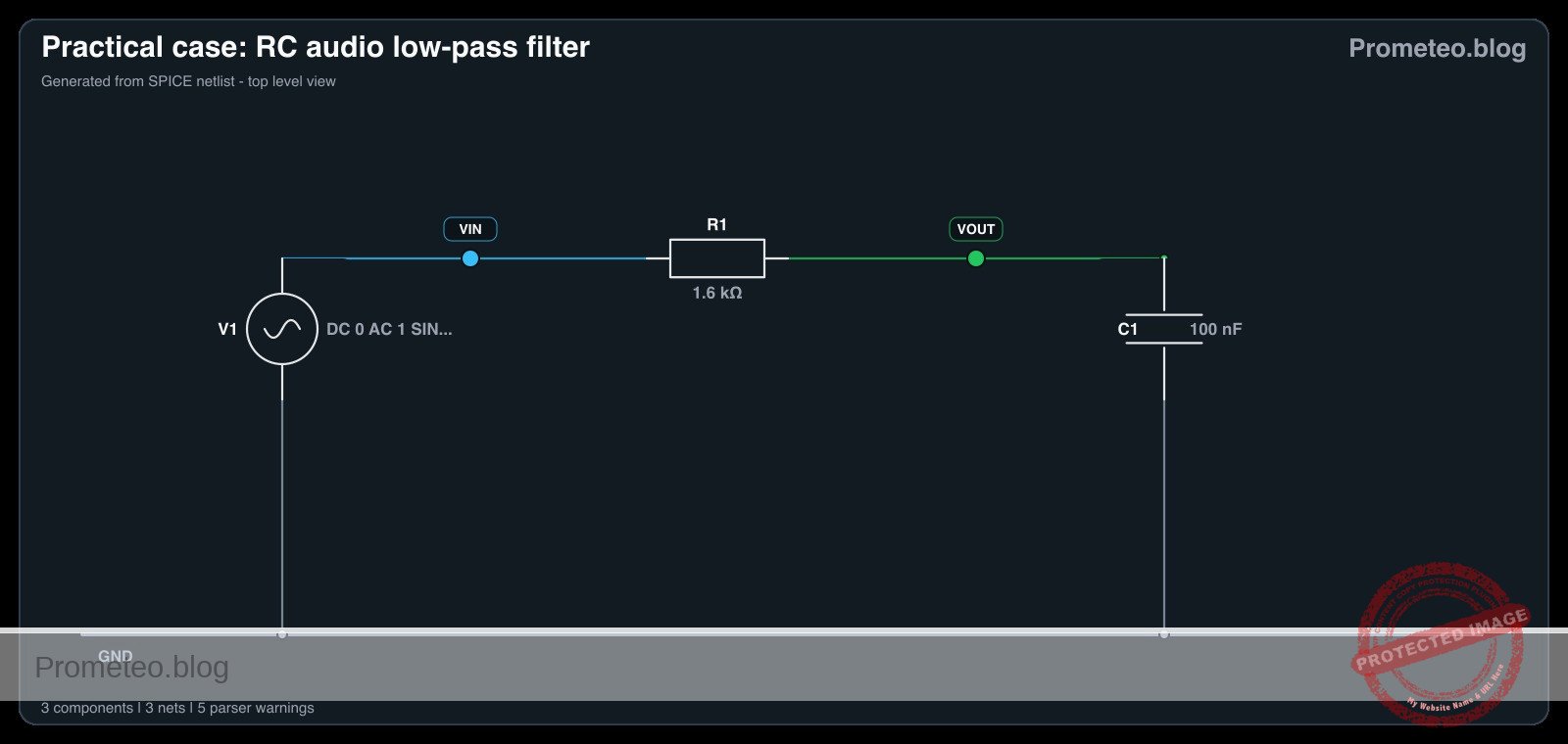
Wiring guide
Construct the circuit using the following connections. Note the explicit node names for analysis.
- V1 (Source): Connect the positive terminal to node
VINand the negative terminal to node0(GND). - R1: Connect one leg to node
VINand the other leg to nodeVOUT. - C1: Connect one leg to node
VOUTand the other leg to node0(GND). - Oscilloscope Ch1: Connect probe tip to
VINand ground clip to0. - Oscilloscope Ch2: Connect probe tip to
VOUTand ground clip to0.
Conceptual block diagram
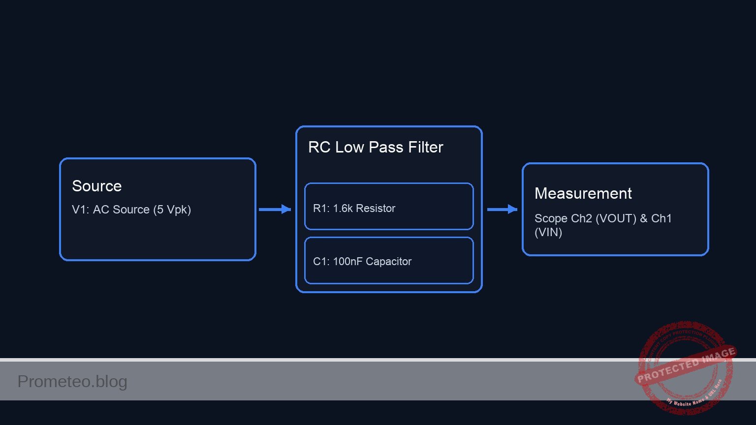
Schematic
[ SIGNAL SOURCE ]               [ RC FILTER STAGE ]                 [ MEASUREMENT ]

                              +--------------------------------------> [ Scope Ch1 (Input) ]
                              |
[ V1: AC Source ] --(VIN)-->--+--> [ R1: 1.6k Resistor ] --(VOUT)-->--+--> [ Scope Ch2 (Output) ]
      (5 Vpk)                                                         |
                                                                      +--> [ C1: 100nF Cap ] --> GND
Electrical diagram
Measurements and tests
Follow these steps to validate the filter design (fc ≈ 1 kHz):
-
Low Frequency Test (Passband):
- Set V1 to 100 Hz.
- Measure Vout peak-to-peak. It should be nearly identical to Vin (approx. 5 V).
-
Cutoff Frequency Verification (fc):
- Increase V1 frequency to 1 kHz.
- Measure Vout. It should drop to approximately 0.707 × Vin (approx. 3.53 V).
- Measure the phase difference between Ch1 and Ch2. Vout should lag Vin by roughly 45°.
-
High Frequency Test (Stopband):
- Set V1 to 10 kHz (one decade above cutoff).
- Measure Vout. The amplitude should be significantly attenuated (approx. 0.5 V or -20 dB relative to input).
-
Bode Plot Analysis (Optional):
- If using a simulation or Bode plotter, sweep from 10 Hz to 100 kHz. Observe the «roll-off» slope of -20 dB/decade after the cutoff point.
SPICE netlist and simulation
Reference SPICE Netlist (ngspice) — excerptFull SPICE netlist (ngspice)
* Practical case: RC audio low-pass filter

* --- Components per BOM and Wiring Guide ---
* V1: AC Voltage Source (Sine Wave, 5 Vpk, 1kHz, AC 1V for Bode)
* Connected: Positive -> VIN, Negative -> 0 (GND)
V1 VIN 0 DC 0 AC 1 SIN(0 5 1000)

* R1: 1.6 kOhm resistor
* Connected: VIN -> VOUT
R1 VIN VOUT 1.6k

* C1: 100 nF capacitor
* Connected: VOUT -> 0 (GND)
C1 VOUT 0 100n

* --- Simulation Commands ---
* Using .control block to sequence analyses and printing correctly in ngspice
.control
    * Transient Analysis: 1kHz signal, run for 5ms
    tran 10u 5ms
* ... (truncated in public view) ...
Copy this content into a .cir file and run with ngspice.
* Practical case: RC audio low-pass filter

* --- Components per BOM and Wiring Guide ---
* V1: AC Voltage Source (Sine Wave, 5 Vpk, 1kHz, AC 1V for Bode)
* Connected: Positive -> VIN, Negative -> 0 (GND)
V1 VIN 0 DC 0 AC 1 SIN(0 5 1000)

* R1: 1.6 kOhm resistor
* Connected: VIN -> VOUT
R1 VIN VOUT 1.6k

* C1: 100 nF capacitor
* Connected: VOUT -> 0 (GND)
C1 VOUT 0 100n

* --- Simulation Commands ---
* Using .control block to sequence analyses and printing correctly in ngspice
.control
    * Transient Analysis: 1kHz signal, run for 5ms
    tran 10u 5ms
    * Print transient results (Oscilloscope)
    print V(VIN) V(VOUT)

    * AC Analysis: Bode Plot, 10 Hz to 100 kHz
    ac dec 10 10 100k
    * Print AC results (Bode Plotter)
    print V(VOUT)

    * Operating Point
    op
.endc

.end
Simulation Results (Transient Analysis)

Show raw data table (512 rows)
Index   time            v(vin)          v(vout)
0	0.000000e+00	0.000000e+00	0.000000e+00
1	1.000000e-07	3.141592e-03	1.962269e-06
2	1.084035e-07	3.405596e-03	2.141025e-06
3	1.252105e-07	3.933604e-03	2.526248e-06
4	1.588245e-07	4.989618e-03	3.462948e-06
5	2.260525e-07	7.101647e-03	6.001184e-06
6	3.605086e-07	1.132570e-02	1.373560e-05
7	6.294206e-07	1.977378e-02	3.982505e-05
8	1.167245e-06	3.666975e-02	1.343969e-04
9	2.242893e-06	7.046023e-02	4.923968e-04
10	4.394190e-06	1.380300e-01	1.878099e-03
11	8.696783e-06	2.730815e-01	7.282571e-03
12	1.730197e-05	5.424874e-01	2.825846e-02
13	2.730197e-05	8.535162e-01	6.884897e-02
14	3.730197e-05	1.161176e+00	1.257276e-01
15	4.730197e-05	1.464254e+00	1.976662e-01
16	5.730197e-05	1.761553e+00	2.834382e-01
17	6.730197e-05	2.051900e+00	3.818193e-01
18	7.730197e-05	2.334149e+00	4.915893e-01
19	8.730197e-05	2.607186e+00	6.115335e-01
20	9.730197e-05	2.869934e+00	7.404442e-01
21	1.073020e-04	3.121356e+00	8.771230e-01
22	1.173020e-04	3.360458e+00	1.020383e+00
23	1.273020e-04	3.586299e+00	1.169049e+00
... (488 more rows) ...
Reference SPICE netlist (ngspice)
* Practical case: RC audio low-pass filter

* --- Components per BOM and Wiring Guide ---
* V1: AC Voltage Source (Sine Wave, 5 Vpk, 1kHz, AC 1V for Bode)
* Connected: Positive -> VIN, Negative -> 0 (GND)
V1 VIN 0 DC 0 AC 1 SIN(0 5 1000)

* R1: 1.6 kOhm resistor
* Connected: VIN -> VOUT
R1 VIN VOUT 1.6k

* C1: 100 nF capacitor
* Connected: VOUT -> 0 (GND)
C1 VOUT 0 100n

* --- Simulation Commands ---
* Using .control block to sequence analyses and printing correctly in ngspice
.control
    * Transient Analysis: 1kHz signal, run for 5ms
    tran 10u 5ms
    * Print transient results (Oscilloscope)
    print V(VIN) V(VOUT)

    * AC Analysis: Bode Plot, 10 Hz to 100 kHz
    ac dec 10 10 100k
    * Print AC results (Bode Plotter)
    print V(VOUT)

    * Operating Point
    op
.endc

.end
Simulation Results (Transient Analysis)
Common mistakes and how to avoid them
- Swapping components (High-Pass vs. Low-Pass):
- Error: Connecting C1 in series and R1 to ground creates a High-Pass filter.
- Solution: Ensure the Capacitor is the component connected between the output node and Ground.
- Ignoring Load Impedance:
- Error: Connecting a low-impedance load (like an 8 Ω speaker) directly to
VOUT. - Solution: This passive filter has high output impedance. Use an op-amp buffer if driving a heavy load.
- Error: Connecting a low-impedance load (like an 8 Ω speaker) directly to
- Using Polarized Capacitors Incorrectly:
- Error: Using an electrolytic capacitor with reverse polarity in an AC circuit without a DC bias.
- Solution: For pure AC audio signals, use non-polarized capacitors (ceramic, film, or bipolar electrolytic).
Troubleshooting
- Symptom: Vout is zero at all frequencies.
- Cause: Short circuit across C1 or open circuit at R1.
- Fix: Check continuity across C1; if it beeps, the capacitor is shorted or the node is grounded accidentally.
- Symptom: No attenuation occurs at high frequencies.
- Cause: C1 is open (broken) or R1 is shorted.
- Fix: Replace C1. Verify R1 measures 1.6 kΩ.
- Symptom: Cutoff frequency is totally wrong.
- Cause: Incorrect component values (e.g., using 100 pF instead of 100 nF).
- Fix: Double-check color codes on resistors and markings on capacitors (104 code = 100 nF).
Possible improvements and extensions
- Second-Order Filter: Cascade two RC stages in series to achieve a steeper roll-off (-40 dB/decade) for better noise rejection.
- Active Low-Pass Filter: Add an Operational Amplifier (Op-Amp) to create an active filter, allowing for signal gain and preventing the load from affecting the filter’s frequency response.
More Practical Cases on Prometeo.blog
Find this product and/or books on this topic on Amazon
As an Amazon Associate, I earn from qualifying purchases. If you buy through this link, you help keep this project running.
Quick Quiz

Telecommunications Electronics Engineer and Computer Engineer (official degrees in Spain).