Level: Medium – Design an RPM measurement system using a photodiode in photoconductive mode to detect light interruptions.
Objective and use case
In this practical case, you will build a non-contact optical sensor circuit that converts light interruptions caused by a rotating propeller into a clean digital pulse stream. The system uses a photodiode in reverse bias (photoconductive mode) to detect light intensity changes, a comparator to digitize the analog signal, and a logic inverter to buffer the output.
Why it is useful:
* Speed Control Systems: Provides feedback for PID controllers to maintain constant motor speed under varying loads.
* Conveyor Belt Monitoring: Detects jams or stoppages by monitoring the rotation of drive rollers.
* Fan Failure Detection: Used in servers and industrial equipment to trigger alarms if cooling fans stop spinning.
* Non-contact Measurement: Allows measurement of high-speed mechanical parts without adding friction or physical wear.
Expected outcome:
* Signal generation: A square wave output (VOUT) where the frequency is proportional to the motor speed.
* Visual indication: An indicator LED flashes in sync with the propeller blade passing (visible at low speeds).
* Voltage levels: The analog sensor voltage swings between ≈ 0 V (dark) and $>2 V$ (light), converted to valid 5 V TTL logic levels at the output.
* Target audience: Electronics students and hobbyists familiar with basic Op-Amps and discrete semiconductors.
Materials
Bill of Materials:
* V1: 5 V DC supply, function: Main circuit power.
* V2: 5 V DC supply, function: Power for the external light source (or shared with V1).
* D1: BPW34 (or generic) Photodiode, function: Light sensor (Reverse biased).
* R1: 100 kΩ resistor, function: Current-to-voltage conversion (Gain resistor).
* RV1: 10 kΩ potentiometer, function: Adjustable reference voltage (VREF) for the comparator.
* U1: LM358 Op-Amp, function: Voltage comparator.
* U2: 74HC04 Hex Inverter, function: Signal buffering and inversion.
* R2: 330 Ω resistor, function: Output LED current limiting.
* D2: Red LED, function: Pulse indicator.
* L1: White LED or Flashlight, function: External light source pointing at D1.
* M1: DC Motor with a propeller/fan, function: Object to measure (cuts the light beam).
Pin-out of the IC used
Selected Chip: 74HC04 (Hex Inverter)
| Pin | Name | Logic Function | Connection in this case |
|---|---|---|---|
| 1 | 1 A | Input | Connected to Comparator Output (VCOMP) |
| 2 | 1Y | Output | Connected to Output Node (VOUT) |
| 7 | GND | Ground | Connected to Circuit Ground (0) |
| 14 | VCC | Power Supply | Connected to VCC (5 V) |
Note: The LM358 Op-Amp pinout is standard (Pin 8: VCC, Pin 4: GND, Pin 3: Non-inverting input, Pin 2: Inverting input, Pin 1: Output).
Wiring guide
Construct the circuit following these node connections. Ensure the photodiode is shielded from ambient light for best results.
-
Power Nodes:
VCC: Connect positive terminal ofV1, Pin 8 ofU1(LM358), Pin 14 ofU2(74HC04), and one side ofRV1.0(GND): Connect negative terminal ofV1, Pin 4 ofU1, Pin 7 ofU2, the other side ofRV1, Anode ofD1, and Cathode ofD2.
-
Sensor Stage (Photoconductive Mode):
VSENS: Connect Cathode ofD1(Photodiode), one end ofR1, and Pin 3 (Non-inverting input) ofU1.- Connect the other end of
R1toVCC. - Note: This configuration creates a voltage divider. When light hits
D1, reverse current flows, dropping voltage atVSENS. Dark = High Voltage (near VCC); Light = Low Voltage.
-
Comparator Stage:
VREF: Connect the wiper (middle pin) ofRV1to Pin 2 (Inverting input) ofU1.VCOMP: Connect Pin 1 (Output) ofU1to Pin 1 (Input 1 A) ofU2.
-
Output Stage:
VOUT: Connect Pin 2 (Output 1Y) ofU2to one end ofR2. This is your measurement point for the oscilloscope.- Connect the other end of
R2to the Anode ofD2(LED).
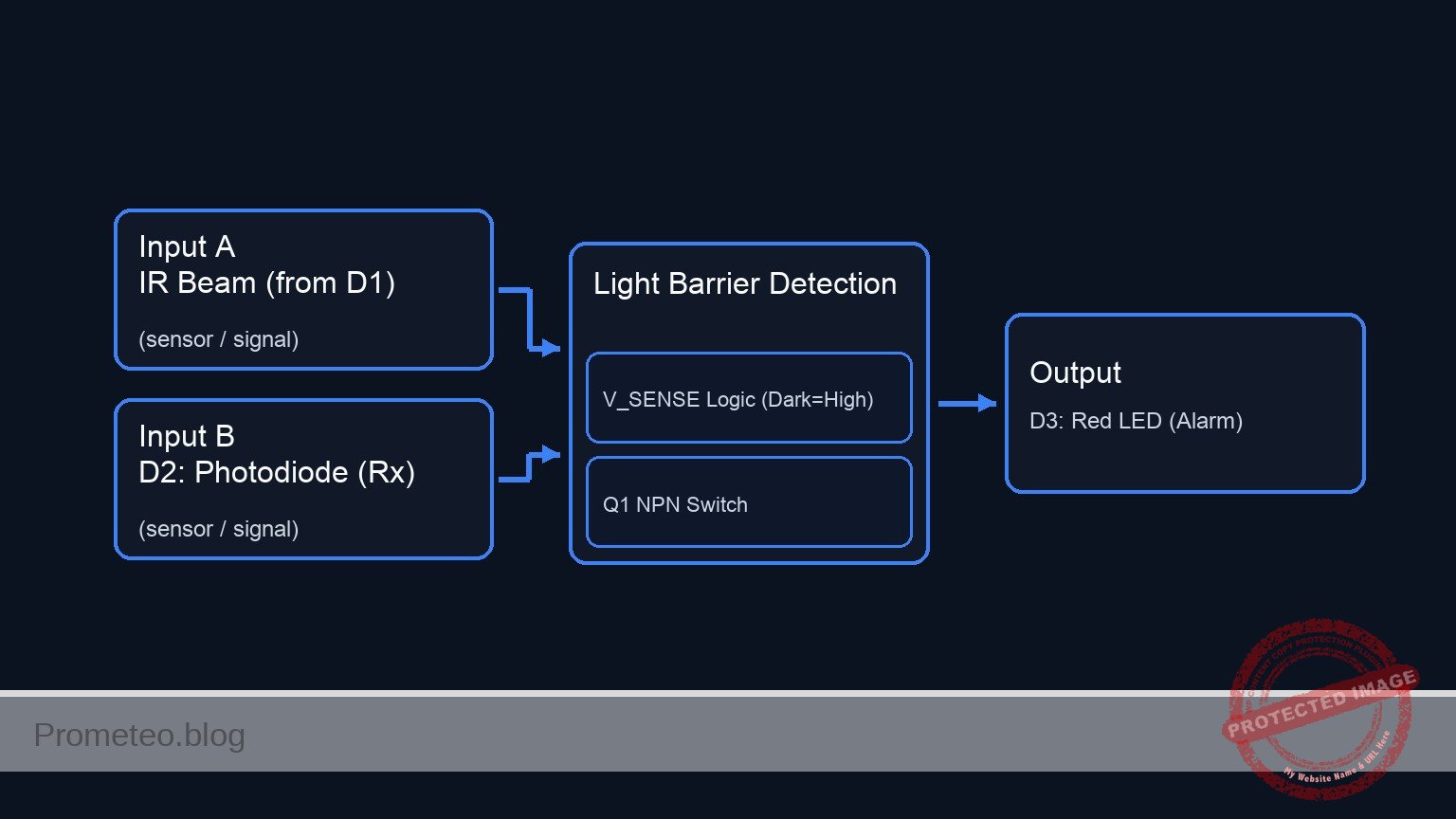
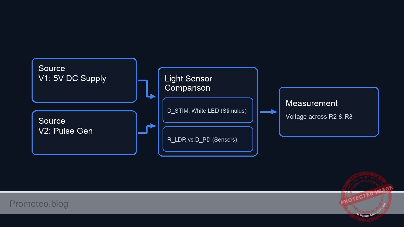
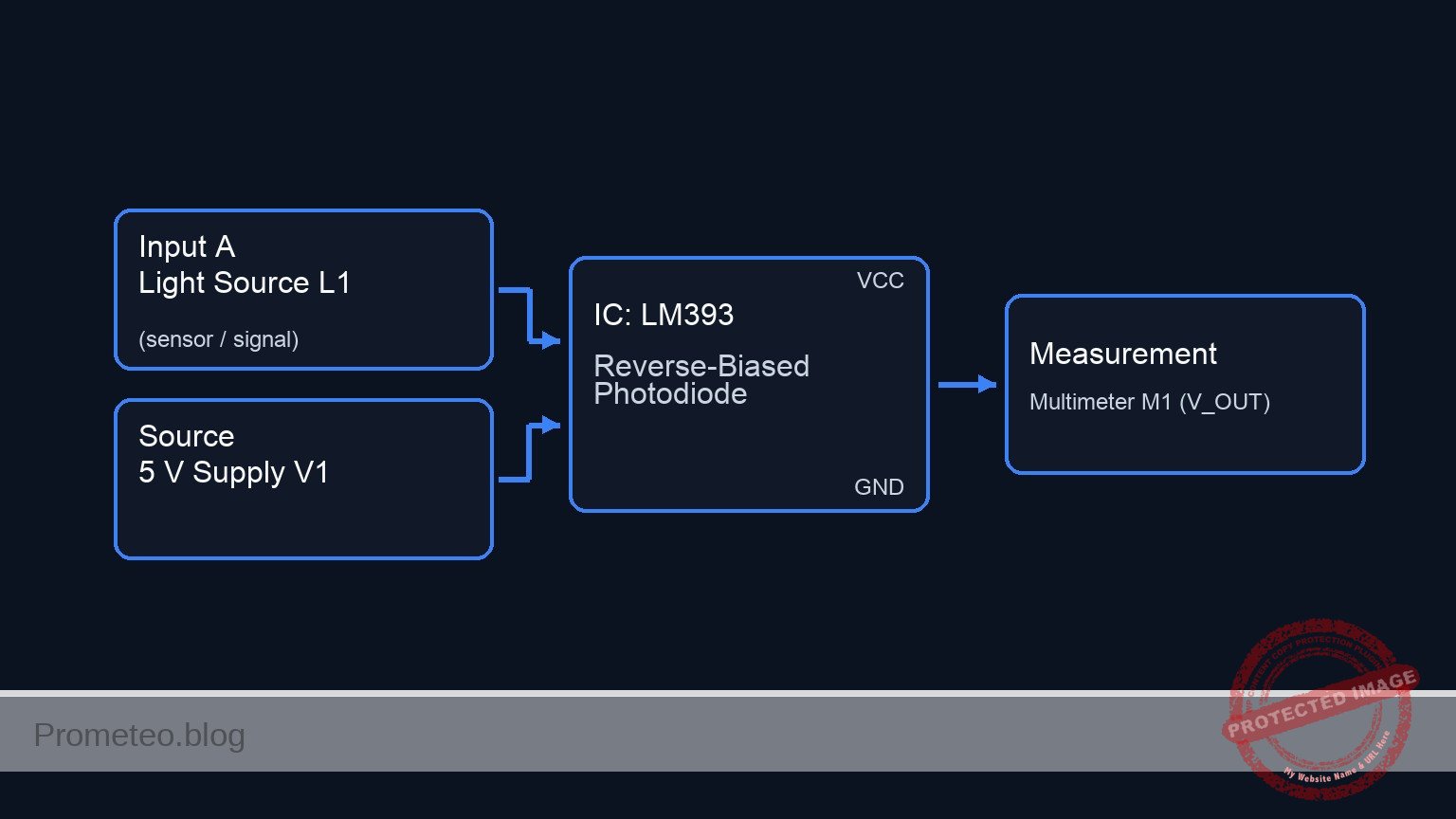
Conceptual block diagram
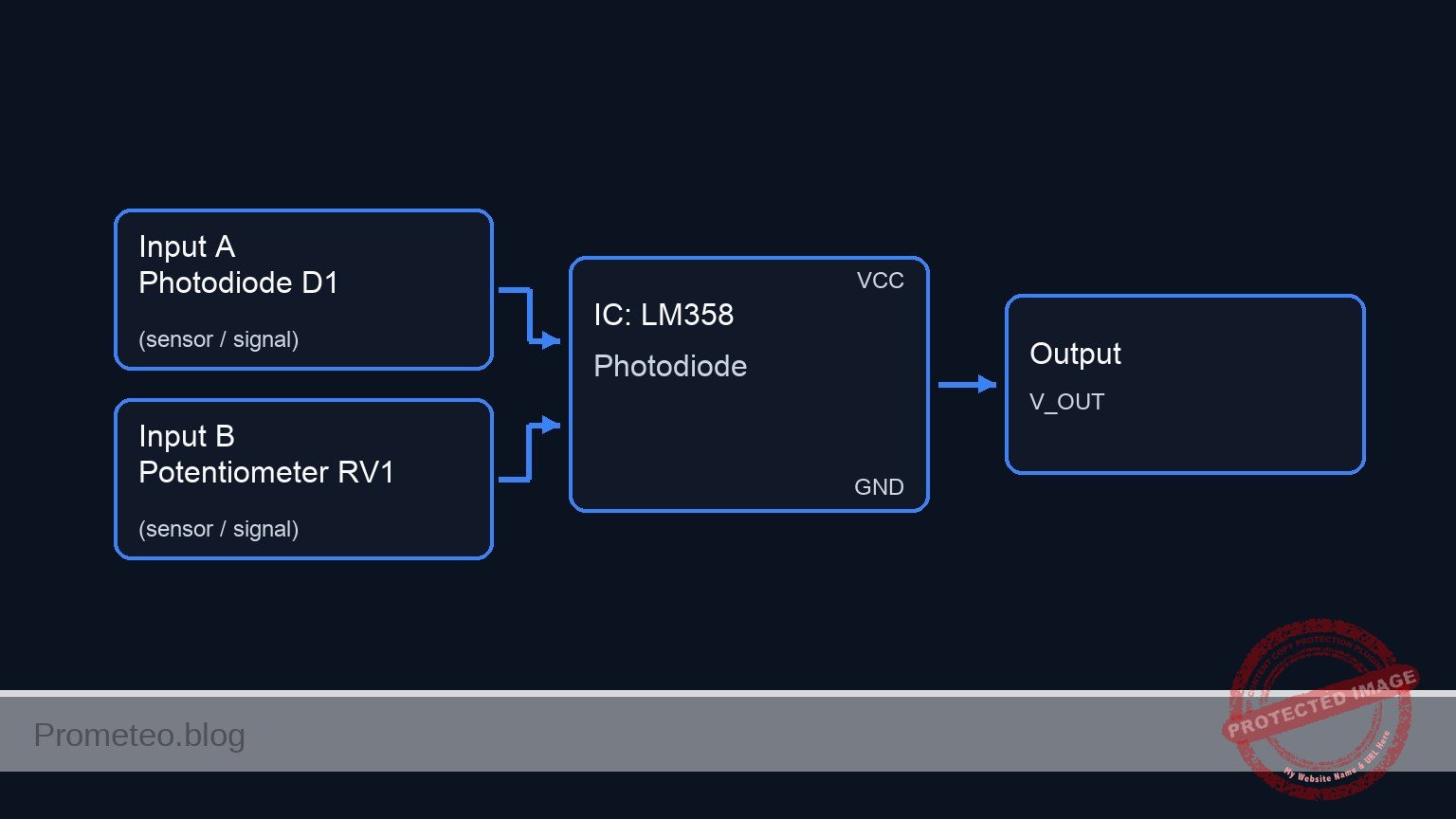
Schematic
Title: Practical case: Optical tachometer for DC motor

      [ INPUTS / SENSORS ]                     [ LOGIC / PROCESSING ]                  [ OUTPUTS ]

[ Light Source L1 ]
        |
   (Light Beam)
        |
        v
[ Motor M1 (Propeller) ]
        |
 (Interrupted Beam)
        |
        v
[ Photodiode D1 ] --(VSENS: Pin 3)-->+----------------+
(Rev-Biased w/ R1)                   |                |
                                     |   U1: LM358    |
                                     |   Comparator   | --(VCOMP: Pin 1)-->+
                                     |                |                    |
[ Potentiometer RV1 ] --(VREF: Pin 2)-->+----------------+                    |
(Adjust Sensitivity)                                                       |
                                                                           v
                                                                   +----------------+
                                                                   |                |
                                                                   |   U2: 74HC04   |
                                                                   |  Hex Inverter  |
                                                                   |                |
                                                                   +-------+--------+
                                                                           |
                                                                     (VOUT: Pin 2)
                                                                           |
                                                                           +--------(Scope Probe)-->
                                                                           |
                                                                           v
                                                                    [ Resistor R2 ]
                                                                           |
                                                                           v
                                                                      [ LED D2 ]
                                                                           |
                                                                           v
                                                                         (GND)
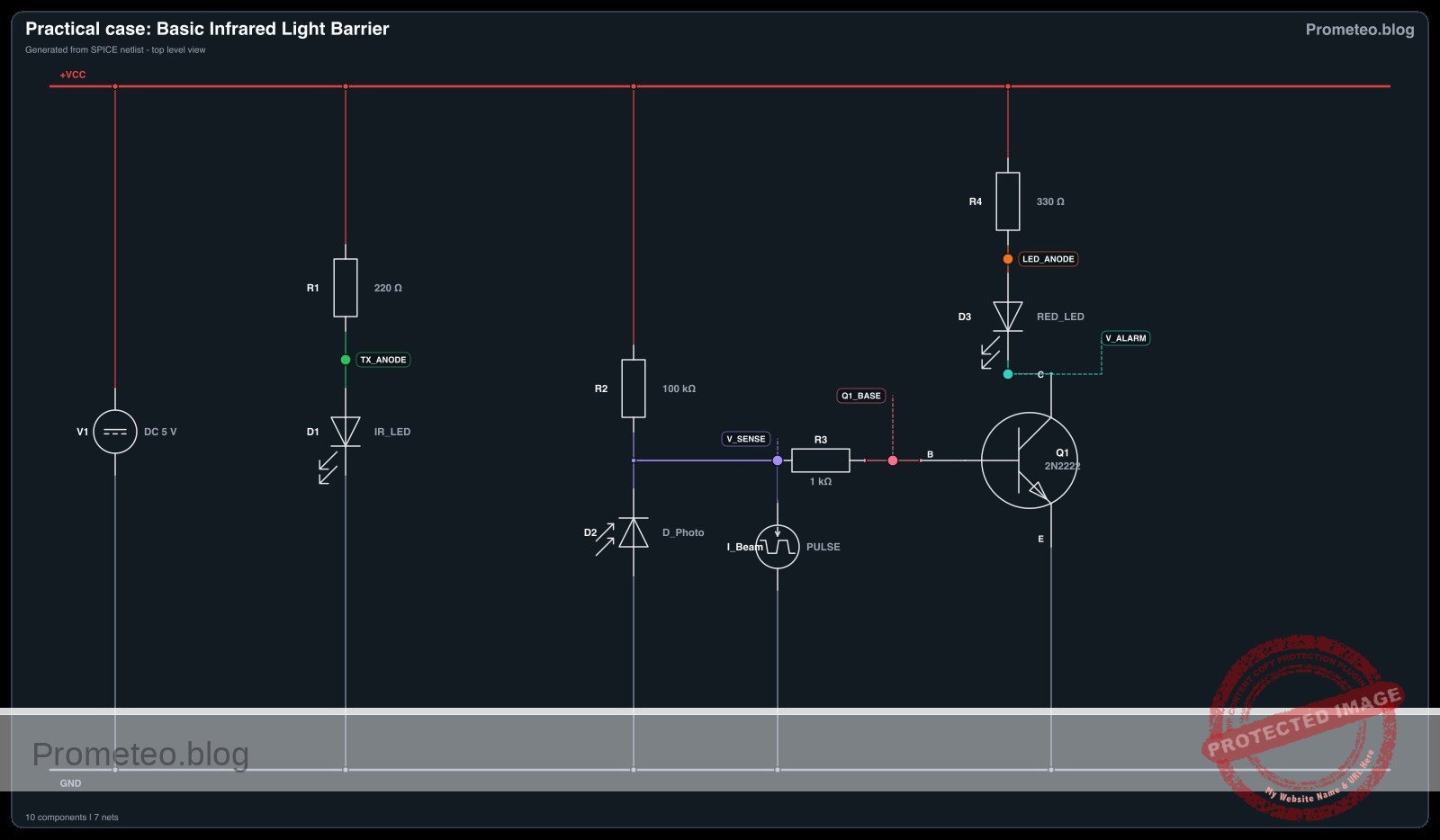
Electrical diagram
Truth table (Logic Stage)
This table describes the logic flow from the physical state to the final electrical output.
| State of Propeller | Light at Photodiode (D1) | Voltage at VSENS |
Comparator Out (VCOMP) |
Inverter Out (VOUT) |
LED (D2) |
|---|---|---|---|---|---|
| Blocking Light | Low / Dark | High (> VREF) | High (Logic 1) | Low (Logic 0) | OFF |
| Pass Through | High / Bright | Low (< VREF) | Low (Logic 0) | High (Logic 1) | ON |
Note: Since the sensor configuration pulls VSENS low when illuminated, the Comparator output goes Low when lit. The 74HC04 inverts this, so the LED turns ON when light passes through.
Measurements and tests
-
Calibration (Static Test):
- Power on the system (
V1= 5 V). - Ensure the light source
L1is shining directly onD1. - Measure
VSENSwith a multimeter. It should be low (e.g., 1 V – 2 V) due to photocurrent. - Block the light with your hand.
VSENSshould rise close toVCC(e.g., 4.5 V). - Adjust potentiometer
RV1so thatVREFis exactly in the middle of these two values (e.g., if Dark=4.5 V and Light=1.5 V, setVREFto 3.0 V).
- Power on the system (
-
Dynamic Test:
- Place the motor
M1so its propeller cuts the beam betweenL1andD1. - Connect Channel 1 of your oscilloscope to
VOUT. - Run the motor. You should see a square wave train.
- Place the motor
-
Calculation:
- Measure the frequency ($f$) of the signal at
VOUTin Hertz. - Count the number of blades ($N$) on your propeller.
- Calculate RPM: RPM = ≤ft( (f / N) \right) × 60.
- Measure the frequency ($f$) of the signal at
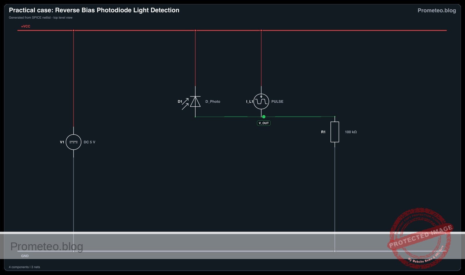
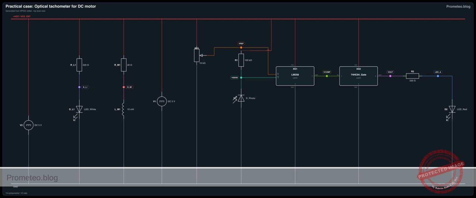
SPICE netlist and simulation
Reference SPICE Netlist (ngspice) — excerptFull SPICE netlist (ngspice)
* Practical case: Optical tachometer for DC motor

* ==========================================
* Models and Definitions
* ==========================================

* Photodiode Model (Generic BPW34)
.model D_BPW34 D(IS=10n N=1.1 RS=5 CJO=20p)

* Output LED Model (Red)
.model LED_Red D(IS=1u N=1.8 RS=5 BV=5 IBV=10u)

* External Light Source LED Model (White)
.model LED_White D(IS=1n N=2.5 RS=10 BV=5 IBV=10u)

* Subcircuit: LM358 Op-Amp (Comparator Mode)
* Pins: OUT INM INP GND VCC
.subckt LM358 OUT INM INP GND VCC
* Dummy resistors to ensure DC path for all pins (avoids floating node warnings)
R_supply VCC GND 100Meg
* ... (truncated in public view) ...
Copy this content into a .cir file and run with ngspice.
* Practical case: Optical tachometer for DC motor

* ==========================================
* Models and Definitions
* ==========================================

* Photodiode Model (Generic BPW34)
.model D_BPW34 D(IS=10n N=1.1 RS=5 CJO=20p)

* Output LED Model (Red)
.model LED_Red D(IS=1u N=1.8 RS=5 BV=5 IBV=10u)

* External Light Source LED Model (White)
.model LED_White D(IS=1n N=2.5 RS=10 BV=5 IBV=10u)

* Subcircuit: LM358 Op-Amp (Comparator Mode)
* Pins: OUT INM INP GND VCC
.subckt LM358 OUT INM INP GND VCC
* Dummy resistors to ensure DC path for all pins (avoids floating node warnings)
R_supply VCC GND 100Meg
R_inM    INM GND 100Meg
R_inP    INP GND 100Meg
* Behavioral Output: High (VCC) if INP > INM, Low (GND) otherwise
B_Out OUT GND V = (V(VCC)-V(GND)) * (1 / (1 + exp(-100 * (V(INP)-V(INM)))))
.ends LM358

* Subcircuit: 74HC04 Hex Inverter (Single Gate)
* Pins: IN OUT GND VCC
.subckt 74HC04_Gate IN OUT GND VCC
* Dummy resistors
R_supply VCC GND 100Meg
R_in     IN  GND 100Meg
* Inverter Logic: High if IN < 2.5V
B_Out OUT GND V = (V(VCC)-V(GND)) * (1 / (1 + exp(100 * (V(IN) - 2.5))))
.ends 74HC04_Gate

* ==========================================
* Circuit Instantiation
* ==========================================

* --- Power Supply Section ---
* V1: 5V DC Supply for the main circuit (VCC)
V1 VCC 0 DC 5

* V2: 5V DC Supply for external components (Motor/Light)
V2 VCC_EXT 0 DC 5

* --- Environment (Physical BOM Components) ---
* L1: White LED (External Light Source)
* Modeled as electrical load on V2. Light emission is implicit.
R_L1 VCC_EXT N_L1 220
D_L1 N_L1 0 LED_White

* M1: DC Motor (Propeller)
* Modeled as electrical load on V2. Rotation is simulated by the chopper signal.
R_M1 VCC_EXT N_M1 20
L_M1 N_M1 0 10m

* Optical Interaction Simulation:
* V_Chopper simulates the propeller cutting the light beam from L1 to D1.
* 1V = Light Passing (Gap), 0V = Light Blocked (Blade).
* Frequency approx 500Hz (2ms period).
V_Chopper V_OPT_LINK 0 PULSE(0 1 0 100u 100u 800u 2000u)

* --- Sensor Stage ---
* R1: 100k Resistor (Pull-up) connecting VCC to VSENS
R1 VCC VSENS 100k

* D1: BPW34 Photodiode
* Wiring: Cathode to VSENS, Anode to GND (Reverse Biased)
D1 0 VSENS D_BPW34

* Photocurrent Injection (Behavioral):
* Represents light hitting D1 when V_OPT_LINK is High.
* Current flows Cathode to Anode (VSENS to GND). I_photo = 50uA.
B_Photo VSENS 0 I = V(V_OPT_LINK) * 50u

* --- Comparator Stage ---
* RV1: 10k Potentiometer (Reference Voltage)
* Configured as 50% divider (5k + 5k) setting VREF to ~2.5V.
R_RV1_Top VCC VREF 5k
R_RV1_Bot VREF 0 5k

* U1: LM358 Op-Amp configured as Comparator
* Pin 8=VCC, Pin 4=GND, Pin 3=VSENS (Non-Inv), Pin 2=VREF (Inv), Pin 1=VCOMP
XU1 VCOMP VREF VSENS 0 VCC LM358

* --- Buffer/Inverter Stage ---
* U2: 74HC04 Hex Inverter (Gate 1)
* Pin 14=VCC, Pin 7=GND, Pin 1=VCOMP (Input), Pin 2=VOUT (Output)
XU2 VCOMP VOUT 0 VCC 74HC04_Gate

* --- Output Stage ---
* R2: 330 Ohm Current Limiting Resistor
R2 VOUT LED_A 330

* D2: Red LED (Signal Indicator)
* Wiring: Anode to R2, Cathode to GND
D2 LED_A 0 LED_Red

* ==========================================
* Analysis Commands
* ==========================================

* Transient analysis: 10ms to capture 5 pulses
.tran 100u 10ms

* Monitor signals
.print tran V(VSENS) V(VREF) V(VCOMP) V(VOUT) V(LED_A) V(V_OPT_LINK)

.end
Simulation Results (Transient Analysis)

Show raw data table (526 rows)
Index   time            v(vsens)        v(vref)         v(vcomp)
0	0.000000e+00	4.994005e+00	2.499938e+00	5.000000e+00
1	1.000000e-06	4.966501e+00	2.499938e+00	5.000000e+00
2	2.000000e-06	4.926705e+00	2.499938e+00	5.000000e+00
3	4.000000e-06	4.836178e+00	2.499938e+00	5.000000e+00
4	8.000000e-06	4.635945e+00	2.499938e+00	5.000000e+00
5	1.600000e-05	4.238426e+00	2.499938e+00	5.000000e+00
6	3.200000e-05	3.442420e+00	2.499938e+00	5.000000e+00
7	6.400000e-05	1.854804e+00	2.499938e+00	4.799431e-28
8	1.000000e-04	8.527235e-02	2.499938e+00	5.000000e-99
9	1.009874e-04	5.613111e-02	2.499938e+00	5.038370e-99
10	1.029622e-04	1.810390e-02	2.499938e+00	5.069277e-99
11	1.055177e-04	3.702381e-03	2.499938e+00	5.376972e-99
12	1.063053e-04	2.444841e-03	2.499938e+00	6.193694e-99
13	1.072769e-04	1.458053e-03	2.499938e+00	5.050362e-99
14	1.083003e-04	8.469348e-04	2.499938e+00	4.694441e-99
15	1.095417e-04	4.347045e-04	2.499938e+00	5.049162e-99
16	1.109578e-04	2.013374e-04	2.499938e+00	4.883316e-99
17	1.123791e-04	9.296145e-05	2.499938e+00	4.945812e-99
18	1.143288e-04	3.056502e-05	2.499938e+00	4.968802e-99
19	1.167173e-04	7.196143e-06	2.499938e+00	4.988316e-99
20	1.202744e-04	2.927790e-07	2.499938e+00	4.996548e-99
21	1.252257e-04	-3.66547e-08	2.499938e+00	4.999835e-99
22	1.343972e-04	1.488928e-08	2.499938e+00	5.000026e-99
23	1.527400e-04	-9.71180e-09	2.499938e+00	4.999988e-99
... (502 more rows) ...
Reference SPICE netlist (ngspice)
* Practical case: Optical tachometer for DC motor

* ==========================================
* Models and Definitions
* ==========================================

* Photodiode Model (Generic BPW34)
.model D_BPW34 D(IS=10n N=1.1 RS=5 CJO=20p)

* Output LED Model (Red)
.model LED_Red D(IS=1u N=1.8 RS=5 BV=5 IBV=10u)

* External Light Source LED Model (White)
.model LED_White D(IS=1n N=2.5 RS=10 BV=5 IBV=10u)

* Subcircuit: LM358 Op-Amp (Comparator Mode)
* Pins: OUT INM INP GND VCC
.subckt LM358 OUT INM INP GND VCC
* Dummy resistors to ensure DC path for all pins (avoids floating node warnings)
R_supply VCC GND 100Meg
R_inM    INM GND 100Meg
R_inP    INP GND 100Meg
* Behavioral Output: High (VCC) if INP > INM, Low (GND) otherwise
B_Out OUT GND V = (V(VCC)-V(GND)) * (1 / (1 + exp(-100 * (V(INP)-V(INM)))))
.ends LM358

* Subcircuit: 74HC04 Hex Inverter (Single Gate)
* Pins: IN OUT GND VCC
.subckt 74HC04_Gate IN OUT GND VCC
* Dummy resistors
R_supply VCC GND 100Meg
R_in     IN  GND 100Meg
* Inverter Logic: High if IN < 2.5V
B_Out OUT GND V = (V(VCC)-V(GND)) * (1 / (1 + exp(100 * (V(IN) - 2.5))))
.ends 74HC04_Gate

* ==========================================
* Circuit Instantiation
* ==========================================

* --- Power Supply Section ---
* V1: 5V DC Supply for the main circuit (VCC)
V1 VCC 0 DC 5

* V2: 5V DC Supply for external components (Motor/Light)
V2 VCC_EXT 0 DC 5

* --- Environment (Physical BOM Components) ---
* L1: White LED (External Light Source)
* Modeled as electrical load on V2. Light emission is implicit.
R_L1 VCC_EXT N_L1 220
D_L1 N_L1 0 LED_White

* M1: DC Motor (Propeller)
* Modeled as electrical load on V2. Rotation is simulated by the chopper signal.
R_M1 VCC_EXT N_M1 20
L_M1 N_M1 0 10m

* Optical Interaction Simulation:
* V_Chopper simulates the propeller cutting the light beam from L1 to D1.
* 1V = Light Passing (Gap), 0V = Light Blocked (Blade).
* Frequency approx 500Hz (2ms period).
V_Chopper V_OPT_LINK 0 PULSE(0 1 0 100u 100u 800u 2000u)

* --- Sensor Stage ---
* R1: 100k Resistor (Pull-up) connecting VCC to VSENS
R1 VCC VSENS 100k

* D1: BPW34 Photodiode
* Wiring: Cathode to VSENS, Anode to GND (Reverse Biased)
D1 0 VSENS D_BPW34

* Photocurrent Injection (Behavioral):
* Represents light hitting D1 when V_OPT_LINK is High.
* Current flows Cathode to Anode (VSENS to GND). I_photo = 50uA.
B_Photo VSENS 0 I = V(V_OPT_LINK) * 50u

* --- Comparator Stage ---
* RV1: 10k Potentiometer (Reference Voltage)
* Configured as 50% divider (5k + 5k) setting VREF to ~2.5V.
R_RV1_Top VCC VREF 5k
R_RV1_Bot VREF 0 5k

* U1: LM358 Op-Amp configured as Comparator
* Pin 8=VCC, Pin 4=GND, Pin 3=VSENS (Non-Inv), Pin 2=VREF (Inv), Pin 1=VCOMP
XU1 VCOMP VREF VSENS 0 VCC LM358

* --- Buffer/Inverter Stage ---
* U2: 74HC04 Hex Inverter (Gate 1)
* Pin 14=VCC, Pin 7=GND, Pin 1=VCOMP (Input), Pin 2=VOUT (Output)
XU2 VCOMP VOUT 0 VCC 74HC04_Gate

* --- Output Stage ---
* R2: 330 Ohm Current Limiting Resistor
R2 VOUT LED_A 330

* D2: Red LED (Signal Indicator)
* Wiring: Anode to R2, Cathode to GND
D2 LED_A 0 LED_Red

* ==========================================
* Analysis Commands
* ==========================================

* Transient analysis: 10ms to capture 5 pulses
.tran 100u 10ms

* Monitor signals
.print tran V(VSENS) V(VREF) V(VCOMP) V(VOUT) V(LED_A) V(V_OPT_LINK)

.end
Simulation Results (Transient Analysis)
Common mistakes and how to avoid them
- Photodiode polarity reversed: In photoconductive mode, the photodiode MUST be reverse-biased (Cathode to positive potential relative to Anode). If connected forward, it acts like a regular diode and won’t sense light effectively.
- Fix: Check the flat side or shorter lead of the photodiode and ensure it connects to the
VSENSnode (which is pulled up to VCC via R1).
- Fix: Check the flat side or shorter lead of the photodiode and ensure it connects to the
- Improper Reference Voltage (
VREF): IfVREFis set too high (above the dark voltage) or too low (below the light voltage), the comparator will never toggle.- Fix: Always measure
VSENSin both dark and light states before settingRV1.
- Fix: Always measure
- Ambient Light Interference: Room lighting (especially fluorescent lights flickering at 50/60Hz) can trigger the sensor falsely.
- Fix: Use an opaque tube (heat shrink or a pen casing) around the photodiode to narrow its field of view strictly to the light source.
Troubleshooting
- Symptom: LED is always ON or always OFF.
- Cause:
VREFis not set correctly or the light source is too weak. - Fix: Retune
RV1. EnsureL1is bright and aligned.
- Cause:
- Symptom: Output signal is jittery or has multiple glitches per pulse.
- Cause: Noisy transitions when the voltage crosses the threshold slowly.
- Fix: Add a small hysteresis resistor (e.g., 1 MΩ) between
VCOMPand Pin 3 ofU1, or ensure the optical transition is sharp (focused beam).
- Symptom:
VSENSdoes not change significantly with light.- Cause:
R1value is too low for the sensitivity ofD1. - Fix: Increase
R1to 220 kΩ or 470 kΩ to increase voltage gain (V = Iphoto × R1).
- Cause:
Possible improvements and extensions
- Hysteresis (Schmitt Trigger): Modify the Op-Amp circuit to include positive feedback. This creates two distinct threshold voltages, making the system immune to noise around the switching point.
- Reflective Sensor Mode: Instead of placing the light source opposite the sensor (transmissive), place them side-by-side. Paint the propeller blades black (non-reflective) and white (reflective). This allows measuring RPM on motors where you cannot access both sides of the blades.
More Practical Cases on Prometeo.blog
Find this product and/or books on this topic on Amazon
As an Amazon Associate, I earn from qualifying purchases. If you buy through this link, you help keep this project running.
Quick Quiz

Telecommunications Electronics Engineer and Computer Engineer (official degrees in Spain).