Level: Medium – Analyze a Graetz bridge to convert AC to pulsating DC and measure total voltage drop.
Objective and use case
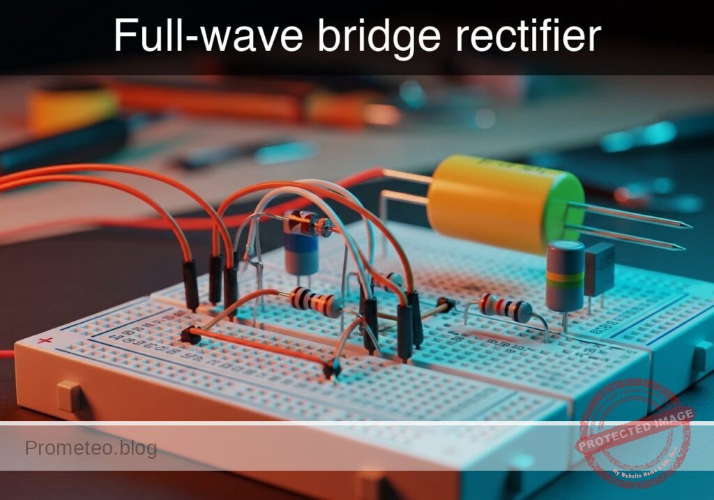
In this practical case, you will build a standard Graetz bridge circuit using four diodes and an AC voltage source to supply a resistive load. This circuit converts an alternating current input (where voltage polarity changes) into a pulsating direct current output (where voltage polarity remains positive).
Why it is useful:
* Power Supplies: It is the fundamental first stage in converting AC mains power to DC for charging laptops, phones, and powering appliances.
* Motor Control: Used in DC motor drives to run motors from an AC supply.
* Polarity Protection: Ensures that a device works correctly regardless of how the input power wires are connected.
* High Efficiency: Utilizes both the positive and negative half-cycles of the AC input, unlike a half-wave rectifier.
Expected outcome:
* Input Signal: A sinusoidal waveform (e.g., 12 V RMS / ~17 V Peak) at 60Hz.
* Output Signal: A series of positive «mounds» (pulsating DC) at 120Hz (double the input frequency).
* Voltage Drop: The peak output voltage will be approximately 1.4 V lower than the peak input voltage due to the forward voltage drop of two diodes in series (2 × 0.7 V).
* Current Flow: Current flows through the load resistor in the same direction during both AC half-cycles.
Target audience and level: Electronics students and hobbyists familiar with basic diode biasing.
Materials
- V1: AC Voltage Source (Amplitude: 17 V [12Vrms], Frequency: 60Hz), function: Input supply
- D1: 1N4007 Diode, function: Rectifier (Bridge arm 1)
- D2: 1N4007 Diode, function: Rectifier (Bridge arm 2)
- D3: 1N4007 Diode, function: Rectifier (Bridge arm 3)
- D4: 1N4007 Diode, function: Rectifier (Bridge arm 4)
- R1: 1 kΩ resistor, function: Output Load
Wiring guide
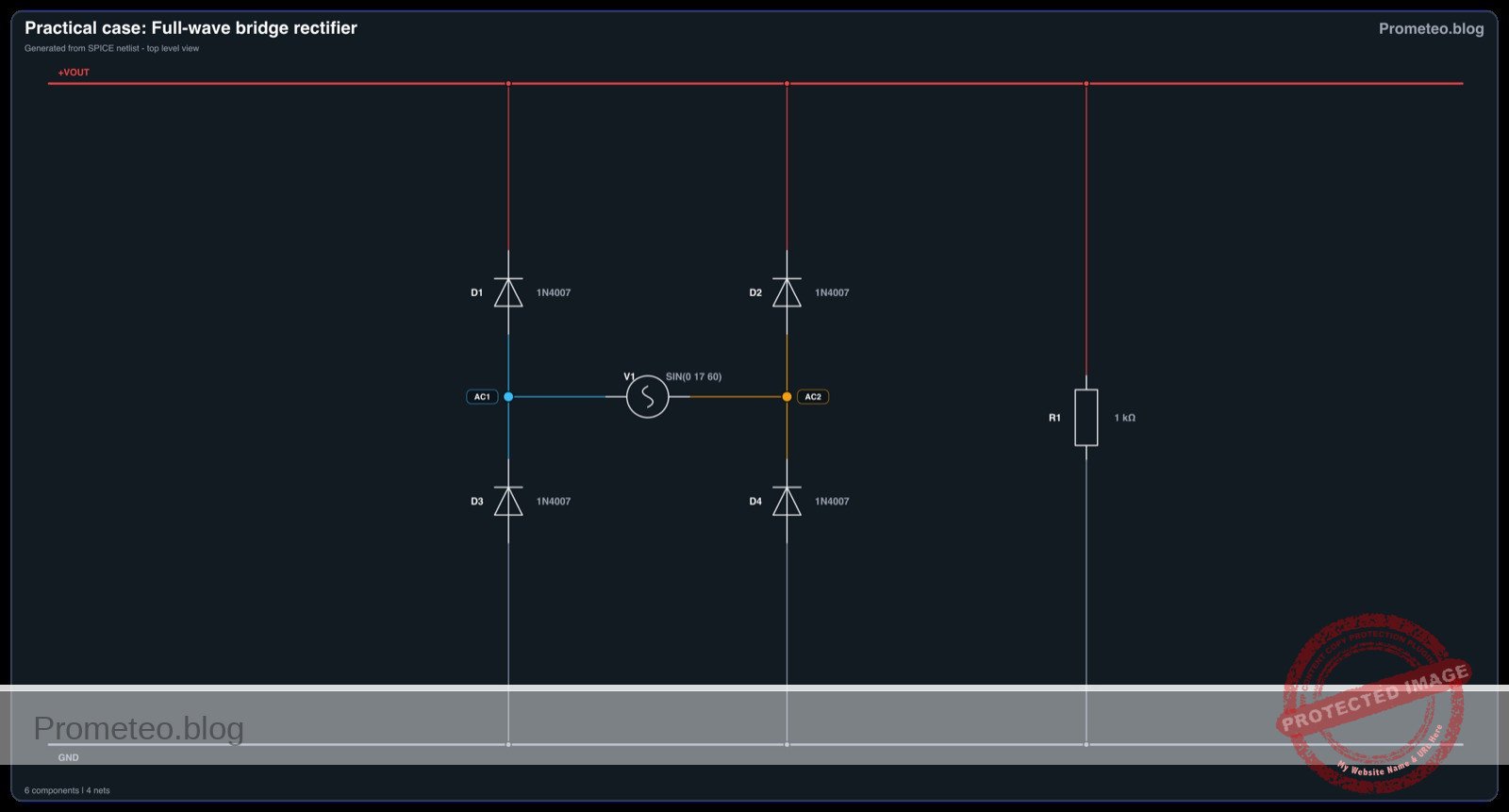
This guide uses specific node names to represent the connections. Ensure the AC source is floating relative to the DC ground to simulate the isolation provided by a transformer.
- V1 (Positive terminal) connects to node
AC1. - V1 (Negative terminal) connects to node
AC2. - D1 (Anode) connects to node
AC1. - D1 (Cathode) connects to node
VOUT. - D2 (Anode) connects to node
AC2. - D2 (Cathode) connects to node
VOUT. - D3 (Anode) connects to node
0(GND). - D3 (Cathode) connects to node
AC1. - D4 (Anode) connects to node
0(GND). - D4 (Cathode) connects to node
AC2. - R1 connects between node
VOUTand node0(GND).
Conceptual block diagram
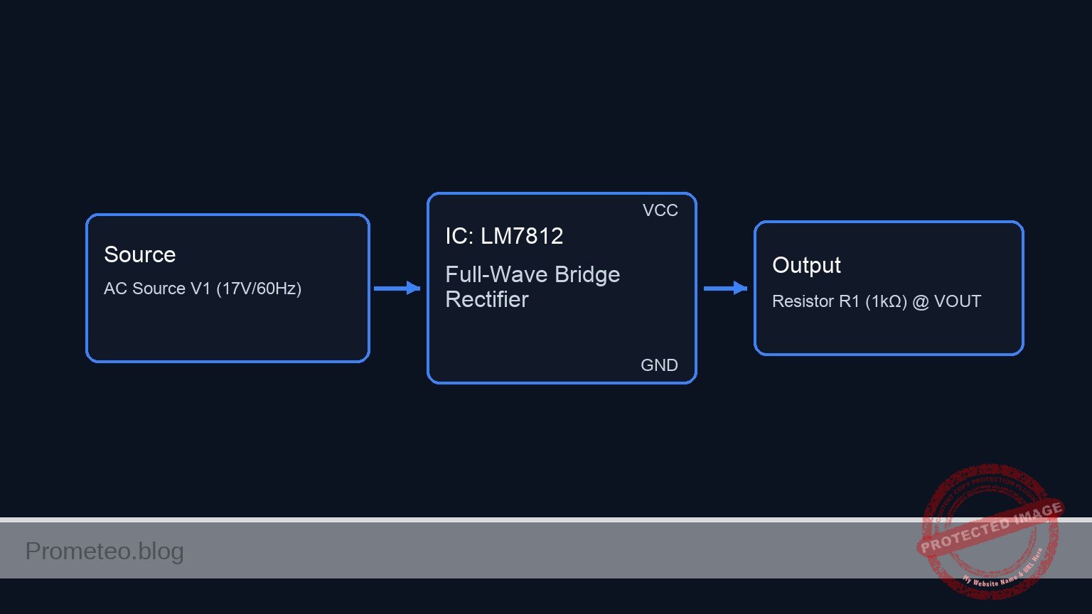
Schematic
[ INPUT SOURCE ]               [ PROCESSING / LOGIC ]               [ OUTPUT LOAD ]

[ AC Source V1 ]
(17 V Amp / 60Hz)
       |
       +----(Node AC1)----->+-----------------------------+
                            |    FULL-WAVE BRIDGE         |
                            |                             |
                            |  [ Diodes D1 & D2 ]         |
                            |  (Direct Positive Peaks)    |--(Node VOUT)--> [ Resistor R1 ]
                            |                             |                 (1 kOhm)
                            |                             |                     |
       +----(Node AC2)----->|  [ Diodes D3 & D4 ]         |                     |
       |                    |  (Direct Negative Peaks)    |                     v
       |                    |  (Create Return Path)       |                    GND
(Source Return)             |                             |
                            +-----------------------------+
                                          |
                                          v
                                     (Node 0/GND)
Electrical diagram
Measurements and tests
Perform the following steps to validate the circuit operation using an oscilloscope or a multimeter:
- Input Verification: Connect channel 1 of the oscilloscope across
AC1andAC2. Verify a full sine wave with a frequency of 60Hz. - Output Visualization: Connect channel 2 of the oscilloscope across
R1(Probe onVOUT, Clip on0). Observe that the negative portions of the sine wave have been «flipped» up, creating a continuous chain of positive pulses. - Frequency Measurement: Measure the frequency of the signal at
VOUT. It should be exactly 120Hz (double the input frequency). - Voltage Drop Analysis: Measure the peak voltage of the Input (Vpeakin) and the peak voltage of the Output (Vpeakout).
- Vpeakout should be approximately Vpeakin – 1.4 V. This accounts for the 0.7 V drop across D1 and 0.7 V drop across D4 (during one cycle) or D2 and D3 (during the other).
SPICE netlist and simulation
Reference SPICE Netlist (ngspice) — excerptFull SPICE netlist (ngspice)
* Title: Practical case: Full-wave bridge rectifier

* --- Component Instantiation ---

* V1: AC Voltage Source (Amplitude: 17 V, Frequency: 60Hz)
* Wiring: V1 (Positive) -> AC1, V1 (Negative) -> AC2
* Note: Source is floating relative to ground (Node 0), connected only to the bridge.
V1 AC1 AC2 SIN(0 17 60)

* D1: 1N4007 Diode (Bridge arm 1)
* Wiring: Anode -> AC1, Cathode -> VOUT
D1 AC1 VOUT 1N4007

* D2: 1N4007 Diode (Bridge arm 2)
* Wiring: Anode -> AC2, Cathode -> VOUT
D2 AC2 VOUT 1N4007

* D3: 1N4007 Diode (Bridge arm 3)
* Wiring: Anode -> 0 (GND), Cathode -> AC1
D3 0 AC1 1N4007
* ... (truncated in public view) ...
Copy this content into a .cir file and run with ngspice.
* Title: Practical case: Full-wave bridge rectifier

* --- Component Instantiation ---

* V1: AC Voltage Source (Amplitude: 17 V, Frequency: 60Hz)
* Wiring: V1 (Positive) -> AC1, V1 (Negative) -> AC2
* Note: Source is floating relative to ground (Node 0), connected only to the bridge.
V1 AC1 AC2 SIN(0 17 60)

* D1: 1N4007 Diode (Bridge arm 1)
* Wiring: Anode -> AC1, Cathode -> VOUT
D1 AC1 VOUT 1N4007

* D2: 1N4007 Diode (Bridge arm 2)
* Wiring: Anode -> AC2, Cathode -> VOUT
D2 AC2 VOUT 1N4007

* D3: 1N4007 Diode (Bridge arm 3)
* Wiring: Anode -> 0 (GND), Cathode -> AC1
D3 0 AC1 1N4007

* D4: 1N4007 Diode (Bridge arm 4)
* Wiring: Anode -> 0 (GND), Cathode -> AC2
D4 0 AC2 1N4007

* R1: 1 kΩ Resistor (Output Load)
* Wiring: VOUT -> 0 (GND)
R1 VOUT 0 1k

* --- Models ---
* Standard model for 1N4007 Rectifier Diode
.model 1N4007 D (IS=7.03n RS=0.034 N=1.81 BV=1000 IBV=0.5u CJO=10p TT=0.1u)

* --- Analysis Commands ---
* Transient analysis: 60Hz period is ~16.6ms.
* Simulating 50ms to capture approximately 3 full cycles.
.tran 50u 50m

* --- Output Directives ---
* Print voltages at AC inputs (relative to GND) and the rectified Output
.print tran V(AC1) V(AC2) V(VOUT)

* Calculate DC operating point
.op

.end
Simulation Results (Transient Analysis)

Show raw data table (1016 rows)
Index   time            v(ac1)          v(ac2)          v(vout)
0	0.000000e+00	3.036573e-18	3.036573e-18	-7.53268e-22
1	5.000000e-07	1.602212e-03	-1.60221e-03	-9.54567e-15
2	1.000000e-06	3.204481e-03	-3.20437e-03	1.126318e-07
3	2.000000e-06	6.409036e-03	-6.40866e-03	3.747988e-07
4	4.000000e-06	1.281816e-02	-1.28172e-02	9.375665e-07
5	8.000000e-06	2.563689e-02	-2.56338e-02	3.056599e-06
6	1.600000e-05	5.127600e-02	-5.12650e-02	1.103556e-05
7	3.200000e-05	1.025657e-01	-1.02513e-01	5.319168e-05
8	6.400000e-05	2.053399e-01	-2.04787e-01	5.532611e-04
9	1.140000e-04	3.725509e-01	-3.57833e-01	1.471794e-02
10	1.640000e-04	5.903791e-01	-4.60003e-01	1.303764e-01
11	2.140000e-04	8.628382e-01	-5.07168e-01	3.556700e-01
12	2.640000e-04	1.155738e+00	-5.33407e-01	6.223310e-01
13	3.140000e-04	1.456815e+00	-5.50867e-01	9.059481e-01
14	3.640000e-04	1.761378e+00	-5.64128e-01	1.197250e+00
15	4.140000e-04	2.068103e+00	-5.74401e-01	1.493702e+00
16	4.640000e-04	2.375673e+00	-5.82891e-01	1.792782e+00
17	5.140000e-04	2.683430e+00	-5.90142e-01	2.093289e+00
18	5.640000e-04	2.990978e+00	-5.96439e-01	2.394538e+00
19	6.140000e-04	3.297988e+00	-6.02000e-01	2.695989e+00
20	6.640000e-04	3.604206e+00	-6.06966e-01	2.997240e+00
21	7.140000e-04	3.909408e+00	-6.11453e-01	3.297955e+00
22	7.640000e-04	4.213406e+00	-6.15537e-01	3.597869e+00
23	8.140000e-04	4.516026e+00	-6.19284e-01	3.896742e+00
... (992 more rows) ...
Reference SPICE netlist (ngspice)
* Title: Practical case: Full-wave bridge rectifier

* --- Component Instantiation ---

* V1: AC Voltage Source (Amplitude: 17 V, Frequency: 60Hz)
* Wiring: V1 (Positive) -> AC1, V1 (Negative) -> AC2
* Note: Source is floating relative to ground (Node 0), connected only to the bridge.
V1 AC1 AC2 SIN(0 17 60)

* D1: 1N4007 Diode (Bridge arm 1)
* Wiring: Anode -> AC1, Cathode -> VOUT
D1 AC1 VOUT 1N4007

* D2: 1N4007 Diode (Bridge arm 2)
* Wiring: Anode -> AC2, Cathode -> VOUT
D2 AC2 VOUT 1N4007

* D3: 1N4007 Diode (Bridge arm 3)
* Wiring: Anode -> 0 (GND), Cathode -> AC1
D3 0 AC1 1N4007

* D4: 1N4007 Diode (Bridge arm 4)
* Wiring: Anode -> 0 (GND), Cathode -> AC2
D4 0 AC2 1N4007

* R1: 1 kΩ Resistor (Output Load)
* Wiring: VOUT -> 0 (GND)
R1 VOUT 0 1k

* --- Models ---
* Standard model for 1N4007 Rectifier Diode
.model 1N4007 D (IS=7.03n RS=0.034 N=1.81 BV=1000 IBV=0.5u CJO=10p TT=0.1u)

* --- Analysis Commands ---
* Transient analysis: 60Hz period is ~16.6ms.
* Simulating 50ms to capture approximately 3 full cycles.
.tran 50u 50m

* --- Output Directives ---
* Print voltages at AC inputs (relative to GND) and the rectified Output
.print tran V(AC1) V(AC2) V(VOUT)

* Calculate DC operating point
.op

.end
Simulation Results (Transient Analysis)
Common mistakes and how to avoid them
- Ground Loops (Scope): Connecting the oscilloscope ground clip to
AC1orAC2while the circuit is mains-referenced can cause a short circuit. Solution: Only connect the scope ground to the common circuit ground (0) at the load, or use a differential probe for the input. - Diode Orientation: Inserting a diode backward in the bridge. Solution: Ensure that two diodes point towards the positive DC output node (
VOUT) and two diodes point away from the ground node (0). - Ignoring Power Ratings: Using a resistor with low wattage for
R1. Solution: Calculate power P = V^2 / R. For 17 V peak, P ≈ 0.3W. Use a 0.5W resistor or greater.
Troubleshooting
- Symptom: The output looks like a half-wave rectifier (gaps between pulses).
- Cause: One of the diodes is open (disconnected or blown).
- Fix: Check continuity of all four diodes; replace the faulty one.
- Symptom: Zero output voltage.
- Cause: Short circuit in the load or open circuit in the source/wiring.
- Fix: Check connections at
AC1andAC2; ensureR1is not shorted.
- Symptom: Input fuse blows or source current is excessive.
- Cause: One or more diodes are shorted, or a diode is installed in reverse (creating a direct path from AC to Ground).
- Fix: Test diodes for shorts using the diode check mode on a multimeter.
Possible improvements and extensions
- Filtering: Add a capacitor (e.g., 470 µF) in parallel with
R1to fill in the gaps between pulses, creating a smooth DC voltage (Ripple reduction). - Regulation: Connect a voltage regulator (like an LM7812 or a Zener diode circuit) after the filter capacitor to produce a constant, stable DC voltage regardless of input fluctuations.
More Practical Cases on Prometeo.blog
Find this product and/or books on this topic on Amazon
As an Amazon Associate, I earn from qualifying purchases. If you buy through this link, you help keep this project running.
Quick Quiz

Telecommunications Electronics Engineer and Computer Engineer (official degrees in Spain).