Level: Basic. Build a safety circuit that cuts a ‘Ready’ signal instantly when a stop button is pressed.
Objective and use case
In this tutorial, you will build a digital logic circuit that inverts an input signal. Specifically, a «System Ready» indicator (Green LED) will remain active by default and will immediately turn off when an emergency pushbutton is pressed.
-
Why it is useful:
- Industrial safety: Simulates an emergency kill switch where the active state shuts down machinery.
- Security systems: Sensors (like door contacts) often break a circuit to trigger an alarm or change a status.
- Fail-safe logic: Ensures a system defaults to «safe» (off) when an active intervention occurs.
-
Expected outcome:
- Idle State: When the button is NOT pressed (Logic 0), the Green LED is ON (Logic 1).
- Active State: When the button IS pressed (Logic 1), the Green LED turns OFF (Logic 0).
- Signal Voltage: Input transitions between 0 V and 5 V; Output inverts logically.
-
Target audience and level: Students and hobbyists learning basic digital inversion.
Materials
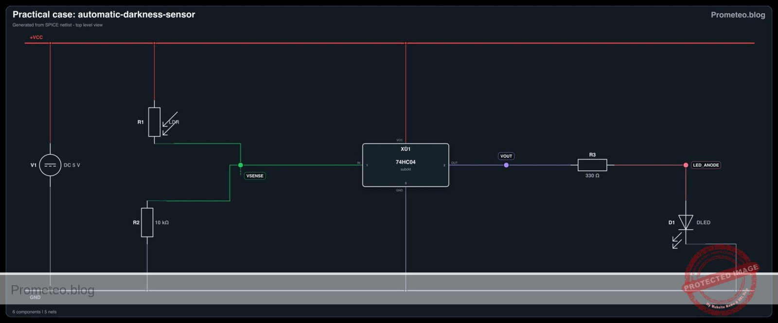
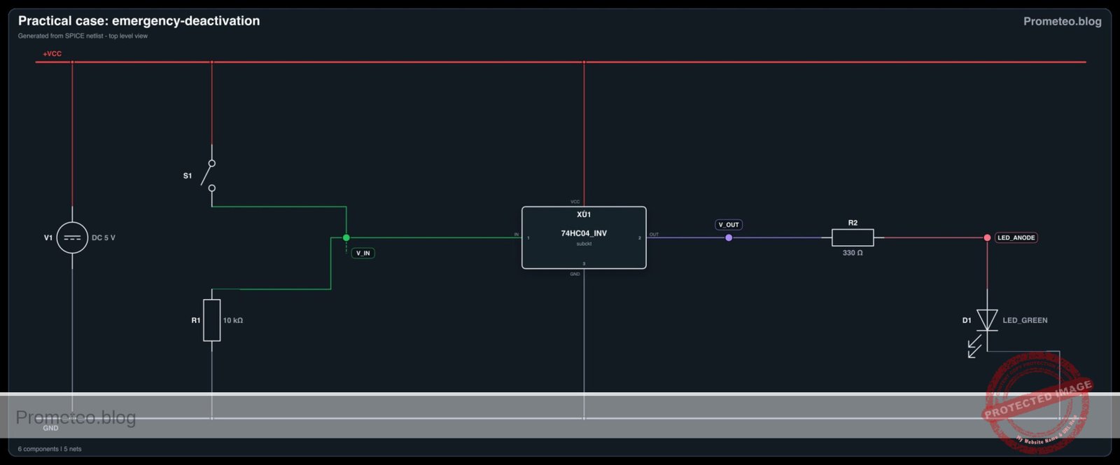
- V1: 5 V DC supply, function: main power source.
- U1: 74HC04 Hex Inverter IC, function: logic inversion (NOT gate).
- S1: Pushbutton (Normally Open), function: emergency signal trigger.
- R1: 10 kΩ resistor, function: pull-down resistor for input stability.
- R2: 330 Ω resistor, function: current limiting for the LED.
- D1: Green LED, function: ‘System Ready’ indicator.
Pin-out of the IC used
Selected Chip: 74HC04 (Hex Inverter)
| Pin | Name | Logic function | Connection in this case |
|---|---|---|---|
| 14 | VCC | Power Supply (+5V) | Connect to 5 V rail |
| 7 | GND | Ground (0V) | Connect to 0 V rail |
| 1 | 1A | Input 1 | Connect to Pushbutton and Pull-down resistor |
| 2 | 1Y | Output 1 | Connect to LED resistor (R2) |
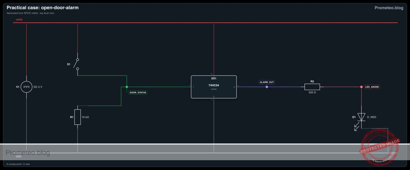
Wiring guide
Construct the circuit following these node connections (Nodes: VCC, 0, V_IN, V_OUT):
- Power Supply:
- V1 connects between
VCC(positive) and0(negative/GND). - U1 Pin 14 connects to
VCC. - U1 Pin 7 connects to
0.
- V1 connects between
- Input Stage (Button Logic):
- S1 connects between
VCCandV_IN. - R1 connects between
V_INand0(This pulls the input to 0 V when the button is open). - U1 Pin 1 (Input 1A) connects to
V_IN.
- S1 connects between
- Output Stage (Indicator):
- U1 Pin 2 (Output 1Y) connects to
V_OUT. - R2 connects between
V_OUTand nodeLED_ANODE. - D1 Anode connects to
LED_ANODE. - D1 Cathode connects to
0.
- U1 Pin 2 (Output 1Y) connects to
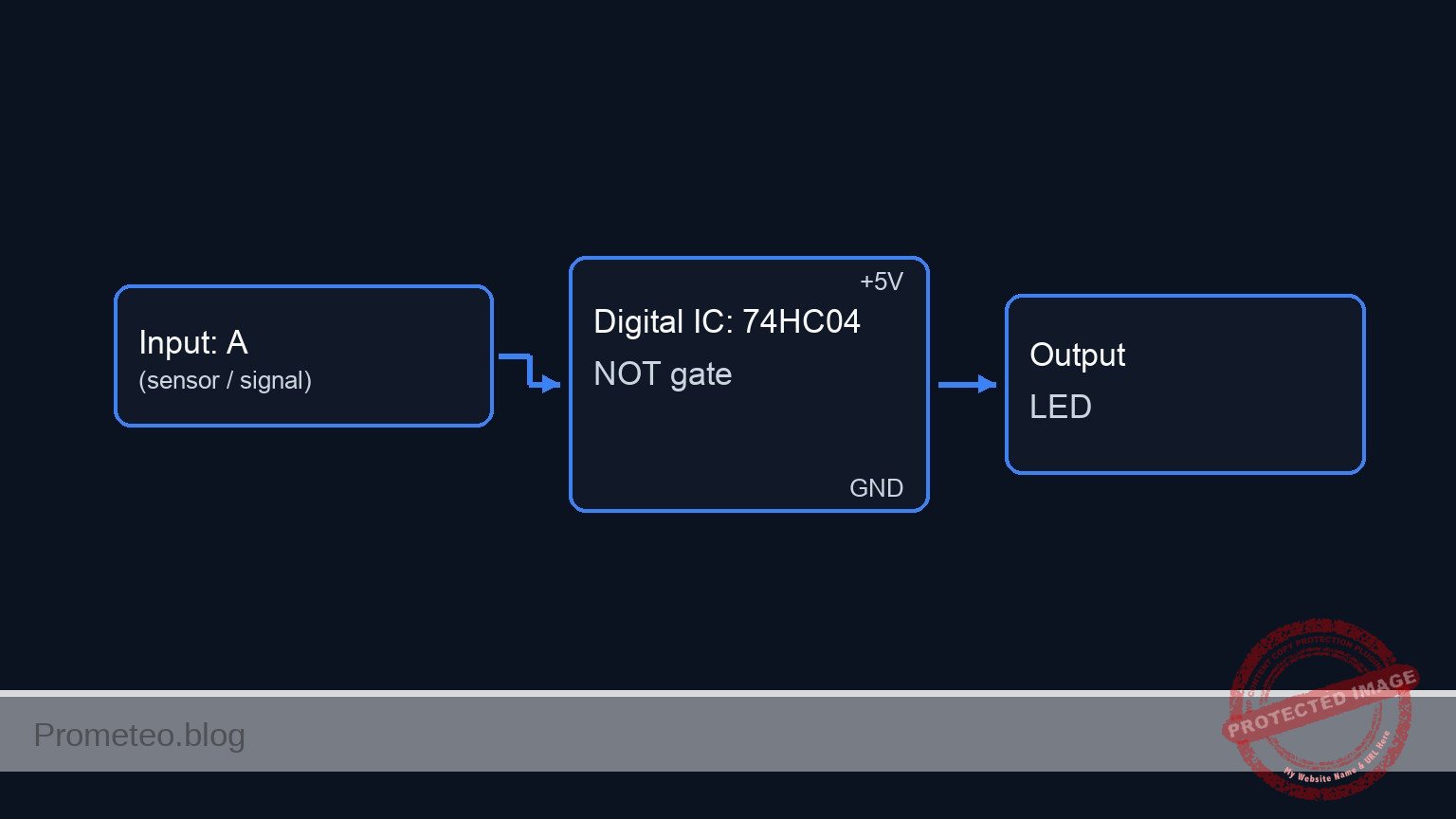
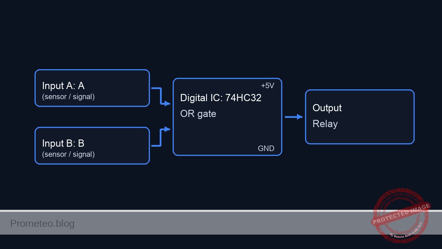
Conceptual block diagram

Schematic
[ INPUT STAGE ]                          [ LOGIC STAGE ]                       [ OUTPUT STAGE ]

    [ V1: 5V Supply ] --(Power VCC)--------> [ U1 Power: Pin 14 ]

    [ S1: Pushbutton ] --(Press = 5V)--+
    (Emergency Trig)                   |
                                       v
                                  [ Node V_IN ] --(Pin 1)--> [   U1: 74HC04   ] --(Pin 2)--> [ R2: 330 Ohm ] --> [ D1: Green LED ] --> [ GND ]
                                       ^                     [ Hex Inverter IC]              (Current Limit)     (System Ready)
                                       |                     [   (NOT Gate)   ]
    [ R1: 10k Resistor ] --(Open = 0V)-+                     [  GND: Pin 7    ]
    (Pull-down to GND)                                             |
                                                                   v
                                                                [ GND ]
Electrical diagram
Truth table
The 74HC04 implements the Boolean NOT function ($Y = \overline{A}$).
| Button State | Input Voltage (V_IN) | Logic Input (A) | Logic Output (Y) | LED State |
|---|---|---|---|---|
| Released | 0 V (Pulled down) | 0 | 1 | ON |
| Pressed | 5 V (VCC) | 1 | 0 | OFF |
Measurements and tests
Follow these steps to validate the emergency deactivation logic:
-
Idle Check:
- Ensure the power supply is on. Do not touch the button.
- Visual: The Green LED should be lit.
- Measurement: Use a multimeter to measure voltage at
V_IN(Pin 1). It should be approx 0 V. - Measurement: Measure voltage at
V_OUT(Pin 2). It should be approx 5 V (Logic High).
-
Activation Check:
- Press and hold the pushbutton S1.
- Visual: The Green LED must turn OFF immediately.
- Measurement: Voltage at
V_INshould rise to 5 V. - Measurement: Voltage at
V_OUTshould drop to approx 0 V (Logic Low).
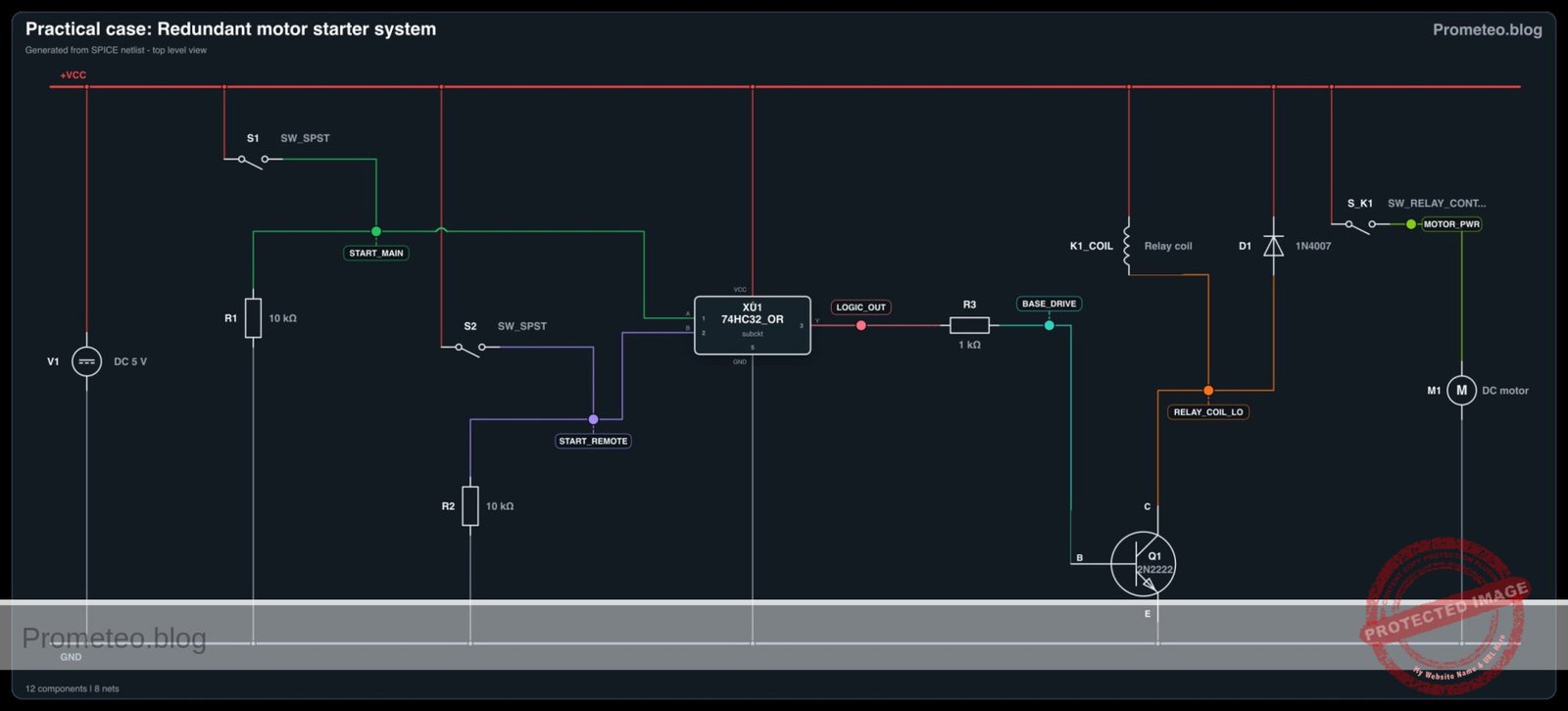
SPICE netlist and simulation
Reference SPICE Netlist (ngspice) — excerptFull SPICE netlist (ngspice)
* Practical case: Emergency deactivation
* Circuit: Inverter Logic (NOT Gate) with LED Indicator

* --- Power Supply ---
* V1: Main 5V DC supply
V1 VCC 0 DC 5

* --- Input Stage (Button Logic) ---
* Components: S1 (Pushbutton), R1 (Pull-down)
* Connectivity: S1 connects VCC to V_IN. R1 connects V_IN to 0.
* Logic:
*   - Button Released (Default): S1 Open -> V_IN pulled to 0V by R1.
*   - Button Pressed (Emergency): S1 Closed -> V_IN pulled to 5V (VCC).

* Simulation of S1 (Normally Open Pushbutton):
* Modeled as a Voltage-Controlled Switch (S1) driven by SW_CTRL.
* Vt=2.5V ensures switch closes when control signal is 5V.
S1 VCC V_IN SW_CTRL 0 SW_BTN
.model SW_BTN SW(Vt=2.5 Vh=0.1 Ron=1 Roff=10Meg)

* ... (truncated in public view) ...
Copy this content into a .cir file and run with ngspice.
* Practical case: Emergency deactivation
* Circuit: Inverter Logic (NOT Gate) with LED Indicator

* --- Power Supply ---
* V1: Main 5V DC supply
V1 VCC 0 DC 5

* --- Input Stage (Button Logic) ---
* Components: S1 (Pushbutton), R1 (Pull-down)
* Connectivity: S1 connects VCC to V_IN. R1 connects V_IN to 0.
* Logic:
*   - Button Released (Default): S1 Open -> V_IN pulled to 0V by R1.
*   - Button Pressed (Emergency): S1 Closed -> V_IN pulled to 5V (VCC).

* Simulation of S1 (Normally Open Pushbutton):
* Modeled as a Voltage-Controlled Switch (S1) driven by SW_CTRL.
* Vt=2.5V ensures switch closes when control signal is 5V.
S1 VCC V_IN SW_CTRL 0 SW_BTN
.model SW_BTN SW(Vt=2.5 Vh=0.1 Ron=1 Roff=10Meg)

* Control Signal (User Finger Simulation):
* Generates a pulse: 0V (Released) -> 5V (Pressed) -> 0V (Released).
* Timeline: Idle for 100us, Press for 300us, then Release.
V_BTN_CTRL SW_CTRL 0 PULSE(0 5 100u 1u 1u 300u 1000u)

* R1: 10k Pull-down resistor
R1 V_IN 0 10k

* --- Logic Stage (U1) ---
* Component: 74HC04 Hex Inverter
* Connectivity: Pin 1 (Input) -> V_IN, Pin 2 (Output) -> V_OUT.
* Power: Pin 14 -> VCC, Pin 7 -> 0.
XU1 V_IN V_OUT 0 VCC 74HC04_INV

* Subcircuit for 74HC04 Inverter
* Behavioral model: Output is High when Input is Low.
* Uses a sigmoid function for smooth switching and convergence.
.subckt 74HC04_INV In Out Gnd Vcc
B1 Out Gnd V = V(Vcc,Gnd) / (1 + exp(50 * (V(In,Gnd) - V(Vcc,Gnd)/2)))
.ends

* --- Output Stage (Indicator) ---
* Components: R2 (Resistor), D1 (Green LED)
* Connectivity: V_OUT -> R2 -> LED_ANODE -> D1 -> 0
* Logic:
*   - V_IN=0 (Ready) -> V_OUT=5 -> LED ON.
*   - V_IN=5 (Emergency) -> V_OUT=0 -> LED OFF.

R2 V_OUT LED_ANODE 330

* D1: Green LED
D1 LED_ANODE 0 LED_GREEN
.model LED_GREEN D(Is=1e-22 Rs=5 N=1.5 Cjo=10p Vj=0.75 M=0.33 BV=5 Ibv=10u)

* --- Simulation Directives ---
* Transient analysis to observe the button press event
.tran 10u 600u

* Output data for analysis
.print tran V(V_IN) V(V_OUT) V(LED_ANODE) V(SW_CTRL)

* Calculate DC operating point
.op

.end
Simulation Results (Transient Analysis)

Show raw data table (260 rows)
Index   time            v(v_in)         v(v_out)        v(led_anode)
0	0.000000e+00	4.995005e-03	5.000000e+00	1.833072e+00
1	6.000000e-08	4.995005e-03	5.000000e+00	1.833072e+00
2	1.200000e-07	4.995005e-03	5.000000e+00	1.833072e+00
3	2.400000e-07	4.995005e-03	5.000000e+00	1.833072e+00
4	4.800000e-07	4.995005e-03	5.000000e+00	1.833072e+00
5	9.600000e-07	4.995005e-03	5.000000e+00	1.833072e+00
6	1.920000e-06	4.995005e-03	5.000000e+00	1.833072e+00
7	3.840000e-06	4.995005e-03	5.000000e+00	1.833072e+00
8	7.680000e-06	4.995005e-03	5.000000e+00	1.833072e+00
9	1.536000e-05	4.995005e-03	5.000000e+00	1.833072e+00
10	2.536000e-05	4.995005e-03	5.000000e+00	1.833072e+00
11	3.536000e-05	4.995005e-03	5.000000e+00	1.833072e+00
12	4.536000e-05	4.995005e-03	5.000000e+00	1.833072e+00
13	5.536000e-05	4.995005e-03	5.000000e+00	1.833072e+00
14	6.536000e-05	4.995005e-03	5.000000e+00	1.833072e+00
15	7.536000e-05	4.995005e-03	5.000000e+00	1.833072e+00
16	8.536000e-05	4.995005e-03	5.000000e+00	1.833072e+00
17	9.536000e-05	4.995005e-03	5.000000e+00	1.833072e+00
18	1.000000e-04	4.995005e-03	5.000000e+00	1.833072e+00
19	1.001000e-04	4.995005e-03	5.000000e+00	1.833072e+00
20	1.002750e-04	4.995005e-03	5.000000e+00	1.833072e+00
21	1.003234e-04	4.995005e-03	5.000000e+00	1.833072e+00
22	1.004082e-04	4.995005e-03	5.000000e+00	1.833072e+00
23	1.004317e-04	4.995005e-03	5.000000e+00	1.833072e+00
... (236 more rows) ...
Common mistakes and how to avoid them
- Floating Input: Omitting R1 (pull-down resistor) causes the input to float when the button is released.
- Solution: Always ensure the input pin is connected to GND via a resistor (e.g., 10 kΩ) when the switch is open.
- LED Reversed: The LED does not light up even when the output is High.
- Solution: Check D1 polarity. The longer leg (Anode) must face the resistor/IC output; the shorter leg (Cathode) goes to Ground.
- Short Circuiting Power: Connecting the button directly between VCC and GND without the gate input in between or wiring the button in parallel with the supply.
- Solution: Follow the node list carefully. The button connects VCC to the Input Pin, not directly to Ground.
Troubleshooting
- Symptom: LED is always ON, pressing the button does nothing.
- Cause: The button is not connected to VCC, or the input pin is permanently grounded.
- Fix: Check continuity across S1 when pressed. Ensure S1 connects to Pin 1.
- Symptom: LED is always OFF.
- Cause: IC not powered, LED reversed, or input permanently connected to VCC.
- Fix: Measure Pin 14 (VCC) and Pin 7 (GND). Check
V_INvoltage; it should be 0 V when the button is released.
- Symptom: LED flickers when your hand gets close to the wire.
- Cause: Floating input (Missing R1).
- Fix: Install the 10 kΩ pull-down resistor securely between Pin 1 and Ground.
Possible improvements and extensions
- Add a «Stop» Indicator: Add a second inverter (or use another gate on the same chip) to drive a Red LED that turns ON when the system is stopped (Output High when Input High).
- Latching Circuit: Replace the simple NOT gate with a Flip-Flop logic circuit so that once the emergency button is pressed, the system stays off even if the button is released, requiring a separate «Reset» button.
More Practical Cases on Prometeo.blog
Find this product and/or books on this topic on Amazon
As an Amazon Associate, I earn from qualifying purchases. If you buy through this link, you help keep this project running.
Quick Quiz

Telecommunications Electronics Engineer and Computer Engineer (official degrees in Spain).