Level: Medium — Design a safety logic circuit that lifts a barrier only when vehicle presence and valid ticket verification occur simultaneously.
Objective and use case
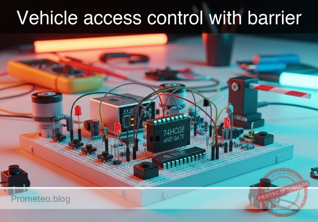
In this practical case, you will build a digital control circuit using a 74HC08 AND gate to simulate the logic of an automated parking barrier. The barrier (represented by an LED) will only activate when a vehicle presence sensor and a ticket validation system trigger simultaneously.
Why it is useful:
* Parking lots: Ensures the gate does not open for pedestrians or if a ticket is invalid.
* Toll booths: Synchronizes payment confirmation with physical vehicle presence.
* Industrial safety: Prevents machinery operation unless a guard is in place and a start command is issued.
* Secure access: Requires dual authentication factors in physical security systems.
Expected outcome:
* State 0 (Rest): LED remains OFF when no buttons are pressed (0 V output).
* State 1 (Partial): LED remains OFF if only the vehicle is detected or only the ticket is validated.
* State 2 (Active): LED turns ON (approx. 5 V / High logic) ONLY when both inputs are active simultaneously.
* Logic Verification: Confirmation of the standard Boolean AND operation ($Y = A \cdot B$).
Target audience and level: Electronics students and hobbyists / Medium.
Materials
- V1: 5 V DC power supply, function: Main circuit power
- U1: 74HC08, function: Quad 2-Input AND Gate IC
- S1: Push-button (NO), function: Simulates «Vehicle Presence Sensor»
- S2: Push-button (NO), function: Simulates «Ticket Validation Signal»
- R1: 10 kΩ resistor, function: Pull-down for Vehicle input
- R2: 10 kΩ resistor, function: Pull-down for Ticket input
- R3: 330 Ω resistor, function: LED current limiting
- D1: Green LED, function: Simulates «Barrier Motor/Open Signal»
- Breadboard and jumper wires
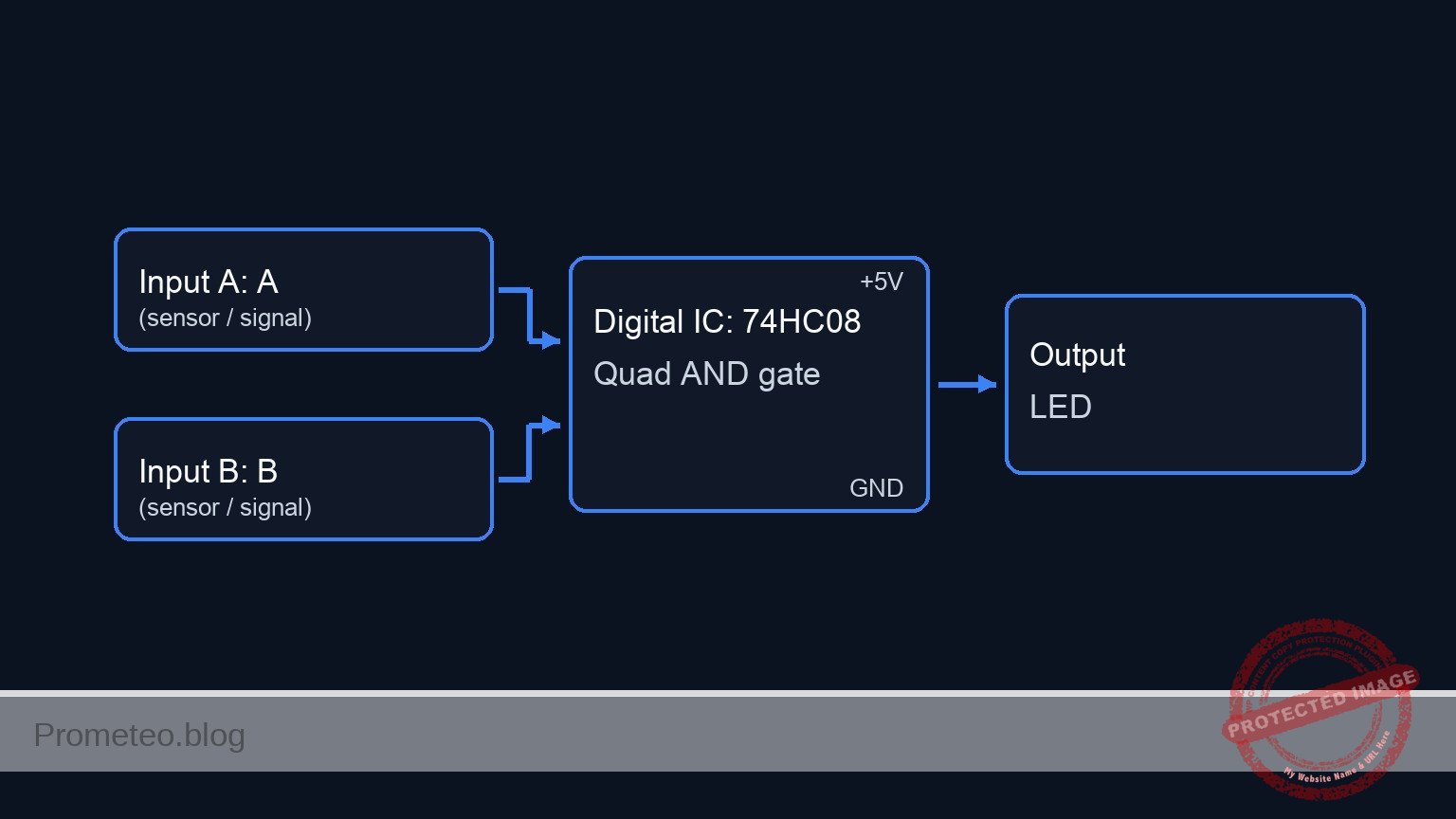
Pin-out of the IC used
Chip: 74HC08 (Quad 2-Input AND Gate)
| Pin | Name | Logic function | Connection in this case |
|---|---|---|---|
| 1 | 1A | Input A | Connected to Vehicle Sensor (S1) |
| 2 | 1B | Input B | Connected to Ticket Validator (S2) |
| 3 | 1Y | Output | Connected to Barrier Indicator (LED) |
| 7 | GND | Ground | Connected to Supply Ground (0 V) |
| 14 | VCC | Power Supply | Connected to +5 V Supply |
Note: Pins 4, 5, 6, 8, 9, 10, 11, 12, and 13 are unused in this specific circuit.
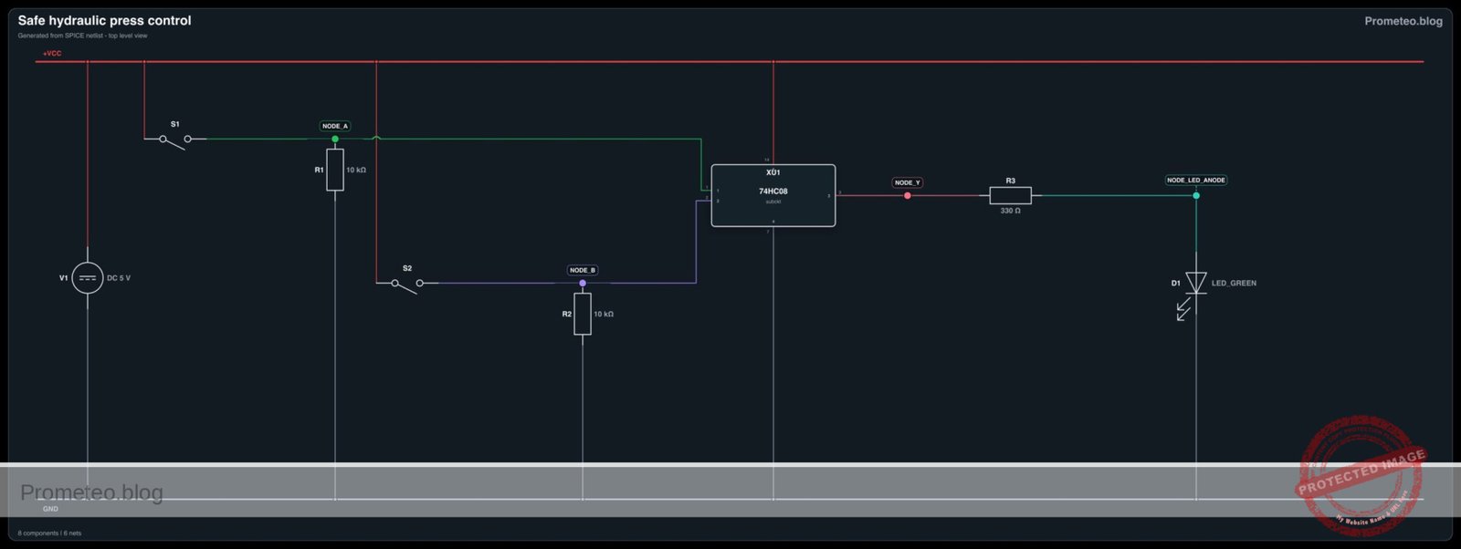
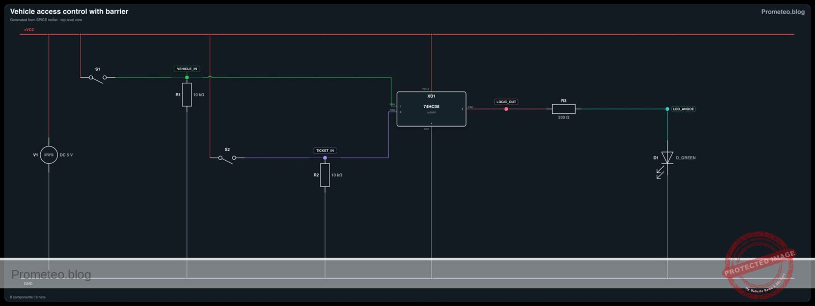
Wiring guide
- Power Supply:
- V1 (+) connects to node
VCC. - V1 (-) connects to node
0(GND).
- V1 (+) connects to node
- IC Power:
- U1 Pin 14 connects to node
VCC. - U1 Pin 7 connects to node
0.
- U1 Pin 14 connects to node
- Input Stage (Vehicle Sensor):
- S1 connects between node
VCCand nodeVEHICLE_IN. - R1 connects between node
VEHICLE_INand node0(active-high configuration). - U1 Pin 1 connects to node
VEHICLE_IN.
- S1 connects between node
- Input Stage (Ticket Validator):
- S2 connects between node
VCCand nodeTICKET_IN. - R2 connects between node
TICKET_INand node0(active-high configuration). - U1 Pin 2 connects to node
TICKET_IN.
- S2 connects between node
- Output Stage (Barrier Actuator):
- U1 Pin 3 connects to node
LOGIC_OUT. - R3 connects between node
LOGIC_OUTand nodeLED_ANODE. - D1 (Anode) connects to node
LED_ANODE. - D1 (Cathode) connects to node
0.
- U1 Pin 3 connects to node
Conceptual block diagram

Schematic
[ INPUT SENSORS ]                     [ LOGIC PROCESSING ]                  [ ACTUATOR OUTPUT ]

 [ VCC ]
    |
 [ S1: Vehicle ]
    |
    +----(Node: VEHICLE_IN)----(Pin 1)-->+----------------------+
    |                                    |                      |
 [ R1: 10k ]                             |      U1: 74HC08      |
    |                                    |      (AND Gate)      |
 [ GND ]                                 |                      |--(Pin 3)--> [ R3: 330 ] --> [ D1: Green LED ] --> [ GND ]
                                         |  (Pin 14: VCC)       |
 [ VCC ]                                 |  (Pin 7:  GND)       |
    |                                    |                      |
 [ S2: Ticket ]                          |                      |
    |                                    |                      |
    +----(Node: TICKET_IN)-----(Pin 2)-->+----------------------+
    |
 [ R2: 10k ]
    |
 [ GND ]
Electrical diagram
Truth table
The 74HC08 follows the standard AND logic verification:
| Vehicle Detected (S1) | Ticket Validated (S2) | Output Voltage (Pin 3) | Barrier State (LED) |
|---|---|---|---|
| Low (0) | Low (0) | ~0 V | Closed (OFF) |
| Low (0) | High (1) | ~0 V | Closed (OFF) |
| High (1) | Low (0) | ~0 V | Closed (OFF) |
| High (1) | High (1) | ~5 V | Open (ON) |
Measurements and tests
- Idle Check: Ensure neither S1 nor S2 is pressed. Measure voltage at U1 Pin 1 and Pin 2 relative to GND. It should read 0 V (Logic Low). The LED must be OFF.
- Single Input Test: Press S1 (Vehicle) only. Measure voltage at Pin 1 (5 V) and Pin 3 (0 V). LED must remain OFF. Repeat for S2 (Ticket).
- Activation Test: Press both S1 and S2 simultaneously. Measure voltage at U1 Pin 3. It should read close to 5 V (Logic High).
- Load Check: Observe the LED turning ON brightly when both buttons are held. This confirms the barrier would lift.
SPICE netlist and simulation
Reference SPICE Netlist (ngspice) — excerptFull SPICE netlist (ngspice)
* TITLE: Practical case: Vehicle access control with barrier
* Ngspice Netlist
* Implements a 74HC08 AND gate circuit with push-button inputs and LED output

* --- Component Models ---
* Switch Model: Voltage Controlled Switch for Push-buttons
* Vt=2.5V (Threshold), Ron=1 ohm (Closed), Roff=100Meg (Open)
.model SW_PUSH SW(Vt=2.5 Ron=1 Roff=100Meg)

* LED Model: Generic Green LED
.model D_GREEN D(Is=1e-22 Rs=5 N=1.5 Cjo=10p BV=5)

* --- Power Supply ---
* V1: 5V DC Main Power Supply
V1 VCC 0 DC 5

* --- Dynamic Stimuli (User Button Presses) ---
* These sources actuate the switches S1 and S2 to simulate user interaction.
* They are not part of the physical circuit but provide the mechanical "push".
* Sequence designed to test Truth Table: 00 -> 10 -> 01 -> 11
* Time unit: microseconds (us)

* S1 Actuator (Vehicle Sensor): Toggles every 200us (starts at 100us)
V_ACT_S1 S1_CTRL 0 PULSE(0 5 100u 1u 1u 100u 200u)

* S2 Actuator (Ticket Validator): Toggles every 400us (starts at 200us)
V_ACT_S2 S2_CTRL 0 PULSE(0 5 200u 1u 1u 200u 400u)

* --- Input Stage: Vehicle Sensor ---
* S1: Push-button connecting VCC to VEHICLE_IN when pressed
* ... (truncated in public view) ...
Copy this content into a .cir file and run with ngspice.
* TITLE: Practical case: Vehicle access control with barrier
* Ngspice Netlist
* Implements a 74HC08 AND gate circuit with push-button inputs and LED output

* --- Component Models ---
* Switch Model: Voltage Controlled Switch for Push-buttons
* Vt=2.5V (Threshold), Ron=1 ohm (Closed), Roff=100Meg (Open)
.model SW_PUSH SW(Vt=2.5 Ron=1 Roff=100Meg)

* LED Model: Generic Green LED
.model D_GREEN D(Is=1e-22 Rs=5 N=1.5 Cjo=10p BV=5)

* --- Power Supply ---
* V1: 5V DC Main Power Supply
V1 VCC 0 DC 5

* --- Dynamic Stimuli (User Button Presses) ---
* These sources actuate the switches S1 and S2 to simulate user interaction.
* They are not part of the physical circuit but provide the mechanical "push".
* Sequence designed to test Truth Table: 00 -> 10 -> 01 -> 11
* Time unit: microseconds (us)

* S1 Actuator (Vehicle Sensor): Toggles every 200us (starts at 100us)
V_ACT_S1 S1_CTRL 0 PULSE(0 5 100u 1u 1u 100u 200u)

* S2 Actuator (Ticket Validator): Toggles every 400us (starts at 200us)
V_ACT_S2 S2_CTRL 0 PULSE(0 5 200u 1u 1u 200u 400u)

* --- Input Stage: Vehicle Sensor ---
* S1: Push-button connecting VCC to VEHICLE_IN when pressed
S1 VCC VEHICLE_IN S1_CTRL 0 SW_PUSH
* R1: 10k Pull-down resistor for Vehicle input
R1 VEHICLE_IN 0 10k

* --- Input Stage: Ticket Validator ---
* S2: Push-button connecting VCC to TICKET_IN when pressed
S2 VCC TICKET_IN S2_CTRL 0 SW_PUSH
* R2: 10k Pull-down resistor for Ticket input
R2 TICKET_IN 0 10k

* --- Logic Stage: U1 (74HC08 Quad 2-Input AND Gate) ---
* Subcircuit representing one gate of the 74HC08 IC
* Pins mapped: 1(A), 2(B), 3(Y), 7(GND), 14(VCC)
.subckt 74HC08_GATE PIN1 PIN2 PIN3 PIN7 PIN14
    * Behavioral AND logic using continuous sigmoid functions for convergence
    * Y = VCC if (A > 2.5V) AND (B > 2.5V)
    B_LOGIC PIN3 PIN7 V = V(PIN14) * (1 / (1 + exp(-50*(V(PIN1)-2.5)))) * (1 / (1 + exp(-50*(V(PIN2)-2.5))))
.ends

* Instantiate U1 connected according to Wiring Guide
* Pin 1->VEHICLE_IN, Pin 2->TICKET_IN, Pin 3->LOGIC_OUT, Pin 7->0, Pin 14->VCC
XU1 VEHICLE_IN TICKET_IN LOGIC_OUT 0 VCC 74HC08_GATE

* --- Output Stage: Barrier Actuator ---
* R3: 330 ohm current limiting resistor
R3 LOGIC_OUT LED_ANODE 330
* D1: Green LED (Anode to R3, Cathode to GND)
D1 LED_ANODE 0 D_GREEN

* --- Simulation Directives ---
* Transient analysis for 500us to capture full sequence
.tran 1u 500u
.op

* Print signals to verify logic:
* Expect LOGIC_OUT to be High (~5V) only when both Inputs are High (300us-400us)
.print tran V(VEHICLE_IN) V(TICKET_IN) V(LOGIC_OUT) V(LED_ANODE)

.end
Simulation Results (Transient Analysis)

Show raw data table (1254 rows)
Index   time            v(vehicle_in)   v(ticket_in)    v(logic_out)
0	0.000000e+00	4.999500e-04	4.999500e-04	1.403014e-108
1	1.000000e-08	4.999500e-04	4.999500e-04	1.403014e-108
2	2.000000e-08	4.999500e-04	4.999500e-04	1.403014e-108
3	4.000000e-08	4.999500e-04	4.999500e-04	1.403014e-108
4	8.000000e-08	4.999500e-04	4.999500e-04	1.403014e-108
5	1.600000e-07	4.999500e-04	4.999500e-04	1.403014e-108
6	3.200000e-07	4.999500e-04	4.999500e-04	1.403014e-108
7	6.400000e-07	4.999500e-04	4.999500e-04	1.403014e-108
8	1.280000e-06	4.999500e-04	4.999500e-04	1.403014e-108
9	2.280000e-06	4.999500e-04	4.999500e-04	1.403014e-108
10	3.280000e-06	4.999500e-04	4.999500e-04	1.403014e-108
11	4.280000e-06	4.999500e-04	4.999500e-04	1.403014e-108
12	5.280000e-06	4.999500e-04	4.999500e-04	1.403014e-108
13	6.280000e-06	4.999500e-04	4.999500e-04	1.403014e-108
14	7.280000e-06	4.999500e-04	4.999500e-04	1.403014e-108
15	8.280000e-06	4.999500e-04	4.999500e-04	1.403014e-108
16	9.280000e-06	4.999500e-04	4.999500e-04	1.403014e-108
17	1.028000e-05	4.999500e-04	4.999500e-04	1.403014e-108
18	1.128000e-05	4.999500e-04	4.999500e-04	1.403014e-108
19	1.228000e-05	4.999500e-04	4.999500e-04	1.403014e-108
20	1.328000e-05	4.999500e-04	4.999500e-04	1.403014e-108
21	1.428000e-05	4.999500e-04	4.999500e-04	1.403014e-108
22	1.528000e-05	4.999500e-04	4.999500e-04	1.403014e-108
23	1.628000e-05	4.999500e-04	4.999500e-04	1.403014e-108
... (1230 more rows) ...
Common mistakes and how to avoid them
- Floating Inputs: Failing to include resistors R1 and R2 causes the inputs to «float,» leading to erratic LED flickering even when buttons are not pressed. Always use pull-down resistors with 74HC series logic.
- Missing Power Connections: Forgetting to connect Pin 14 (VCC) and Pin 7 (GND) is a classic error. Logic chips will not function without power, even if inputs are wired correctly.
- LED Without Resistor: Connecting the LED directly to the logic output (Pin 3) without R3 can damage the LED or the 74HC08 output stage due to excessive current.
Troubleshooting
- Symptom: The LED is always ON, even when buttons are released.
- Cause: Missing pull-down resistors or inputs connected directly to VCC.
- Fix: Ensure R1 and R2 are installed correctly between the inputs and GND.
- Symptom: The LED does not light up when both buttons are pressed.
- Cause: LED polarity reversed or IC not powered.
- Fix: Check D1 orientation (flat side is cathode/GND) and measure 5 V across Pins 14 and 7.
- Symptom: LED is very dim when active.
- Cause: Current limiting resistor (R3) value is too high.
- Fix: Ensure R3 is 330 Ω (orange-orange-brown). If it is 10 kΩ or higher, the LED will be barely visible.
Possible improvements and extensions
- Emergency Stop: Introduce a third input using a 3-input AND gate (74HC11) or cascading another 74HC08 gate, connected to a «Stop» switch that overrides the open command.
- Motor Driver Interface: Replace the LED with an NPN transistor (e.g., 2N2222) and a relay to drive a real DC motor or solenoid, simulating a heavy-duty barrier mechanism.
More Practical Cases on Prometeo.blog
Find this product and/or books on this topic on Amazon
As an Amazon Associate, I earn from qualifying purchases. If you buy through this link, you help keep this project running.
Quick Quiz

Telecommunications Electronics Engineer and Computer Engineer (official degrees in Spain).