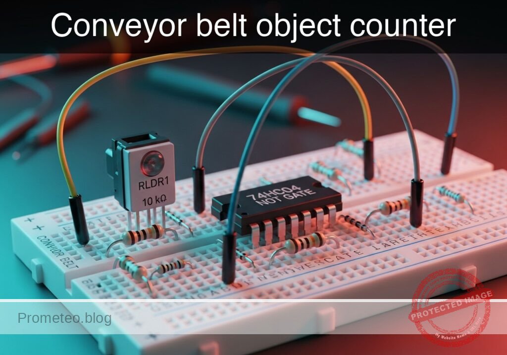
Level: Medium – Build an optical object counter with decimal outputs and an automatic batch reset.
Objective and use case
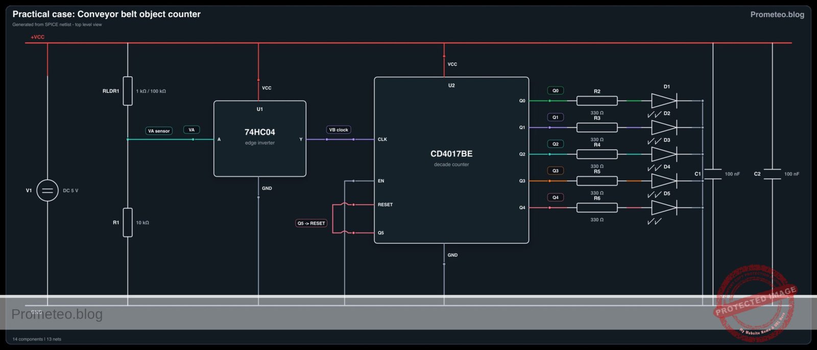
In this practical case, you will build a sequential optical counting circuit using a Light Dependent Resistor (LDR), a 74HC04 inverter for signal conditioning, and a CD4017BE decade counter. The circuit detects objects breaking a light beam, counts them sequentially using LED indicators, and automatically resets after a batch of 5 items.
This circuit is highly relevant in real-world scenarios:
– Packaging lines: Automatically grouping products into predetermined batch sizes (e.g., 5 items per box).
– Industrial automation: Tracking the movement of discrete parts along a conveyor belt.
– Safety interlocks: Monitoring limit switches or optical barriers to ensure an operation cycle is fully completed.
Expected outcome:
– The LDR voltage divider will swing from HIGH (illuminated) to LOW (beam blocked).
– The 74HC04 inverter will generate a clean, rising clock edge (VB) upon each detection.
– The CD4017BE counter will advance its active logic HIGH signal across outputs Q0 to Q4, lighting up LEDs in sequence.
– When the 6th object is detected (count of 5), output Q5 will trigger the reset pin, instantaneously clearing the count back to 0.
Target audience: Electronics students learning sequential logic, decimal counters, and basic sensor integration.
Materials
- V1: 5 V DC supply
- RLDR1: Light Dependent Resistor (LDR), function: optical sensing
- R1: 10 kΩ resistor, function: voltage divider pull-down for LDR
- U1: 74HC04, function: logic inverter and clock edge sharpener
- U2: CD4017BE, function: decade counter with decoded outputs
- D1: red LED, function: count 0 indicator
- D2: red LED, function: count 1 indicator
- D3: red LED, function: count 2 indicator
- D4: red LED, function: count 3 indicator
- D5: red LED, function: count 4 indicator
- R2: 330 Ω resistor, function: LED D1 current limiting
- R3: 330 Ω resistor, function: LED D2 current limiting
- R4: 330 Ω resistor, function: LED D3 current limiting
- R5: 330 Ω resistor, function: LED D4 current limiting
- R6: 330 Ω resistor, function: LED D5 current limiting
- C1: 100 nF capacitor, function: U1 decoupling
- C2: 100 nF capacitor, function: U2 decoupling
Pin-out of the IC used
74HC04 (Hex Inverter)
| Pin | Name | Logic function | Connection in this case |
|---|---|---|---|
| 1 | 1A | Input | Connects to the LDR divider (VA) |
| 2 | 1Y | Output | Connects to the U2 clock input (VB) |
| 7 | GND | Ground | Connects to 0 |
| 14 | VCC | Power | Connects to VCC |
CD4017BE (Decade Counter / Divider)
| Pin | Name | Logic function | Connection in this case |
|---|---|---|---|
| 14 | CLK | Clock input | Connects to the inverted sensor signal (VB) |
| 13 | CKE | Clock enable | Connects to 0 (active low) |
| 15 | RST | Reset | Connects to Q5 (VC) for automatic reset |
| 3 | Q0 | Output 0 | Connects to the D1 branch (V_Q0) |
| 2 | Q1 | Output 1 | Connects to the D2 branch (V_Q1) |
| 4 | Q2 | Output 2 | Connects to the D3 branch (V_Q2) |
| 7 | Q3 | Output 3 | Connects to the D4 branch (V_Q3) |
| 10 | Q4 | Output 4 | Connects to the D5 branch (V_Q4) |
| 1 | Q5 | Output 5 | Connects to reset (VC) |
| 8 | VSS | Ground | Connects to 0 |
| 16 | VDD | Power | Connects to VCC |
Note: Pins 5, 6, 9, 11 and 12 are unused decoded outputs and carry-out pins; leave them floating in this case.
Wiring guide
- V1 connects between
VCCand0. - RLDR1 connects between
VCCandVA. - R1 connects between
VAand0. - U1 pin 14 connects to
VCC. - U1 pin 7 connects to
0. - U1 pin 1 connects to
VA. - U1 pin 2 connects to
VB. - U2 pin 16 connects to
VCC. - U2 pin 8 connects to
0. - U2 pin 13 connects to
0. - U2 pin 14 connects to
VB. - U2 pin 1 connects to
VC. - U2 pin 15 connects to
VC. - U2 pin 3 connects to
V_Q0. - U2 pin 2 connects to
V_Q1. - U2 pin 4 connects to
V_Q2. - U2 pin 7 connects to
V_Q3. - U2 pin 10 connects to
V_Q4. - R2 connects between
V_Q0andV_D1. - D1 connects between
V_D1and0. - R3 connects between
V_Q1andV_D2. - D2 connects between
V_D2and0. - R4 connects between
V_Q2andV_D3. - D3 connects between
V_D3and0. - R5 connects between
V_Q3andV_D4. - D4 connects between
V_D4and0. - R6 connects between
V_Q4andV_D5. - D5 connects between
V_D5and0. - C1 connects between
VCCand0. - C2 connects between
VCCand0.
Conceptual block diagram
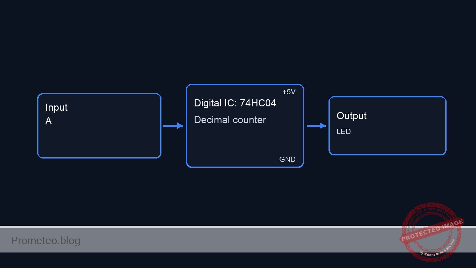
Schematic
[ U2: CD4017BE Decade Counter ]
                                                             |                             |
VCC --> [ RLDR1: LDR ] --(VA)--> [ U1: 74HC04 Inverter ] --(VB)--> CLK (Pin 14)            |
                           |                                 |                  Q0 (Pin 3)-|--(V_Q0)--> [ R2: 330 ] --> [ D1: Red LED ] --> GND
                           +---> [ R1: 10k ] --> GND         |                  Q1 (Pin 2)-|--(V_Q1)--> [ R3: 330 ] --> [ D2: Red LED ] --> GND
                                                             |                  Q2 (Pin 4)-|--(V_Q2)--> [ R4: 330 ] --> [ D3: Red LED ] --> GND
                                                 +--(VC)---------> RST (Pin 15) Q3 (Pin 7)-|--(V_Q3)--> [ R5: 330 ] --> [ D4: Red LED ] --> GND
                                                 |           |                  Q4 (Pin 10)|--(V_Q4)--> [ R6: 330 ] --> [ D5: Red LED ] --> GND
                                                 +---------------< Q5 (Pin 1)              |
                                                             |                             |
                                                 GND ------------> EN (Pin 13)             |
                                                             [-----------------------------]

* Power & Decoupling Notes:
  VCC --> [ C1: 100nF ] --> GND  (U1 Decoupling)
  VCC --> [ C2: 100nF ] --> GND  (U2 Decoupling)
  U1 Power: Pin 14 (VCC), Pin 7 (GND)
  U2 Power: Pin 16 (VCC), Pin 8 (GND)
Electrical diagram
Measurements and tests
- Sensor Calibration: Measure node
VAwith a multimeter. Ensure it rests at >4.0 V when the light source shines on the LDR, and drops to <1.0 V when an object blocks the beam. Adjust R1 if your LDR has different resistance characteristics. - Clock Edge Verification: Connect an oscilloscope to node
VB. Pass an object through the beam and confirm a sharp, clean transition from 0 V to 5 V. - Sequential Counting Check: Monitor nodes
V_Q0throughV_Q4. Verify that each output successively jumps to ~5 V upon each clock pulse, lighting up D1 through D5 one by one. - Auto-Reset Validation: Using an oscilloscope, monitor
VC(Reset). When the 6th object passes, capture the brief microsecond high pulse onVCthat clears the counter back to D1.
SPICE netlist and simulation
Reference SPICE Netlist (ngspice) — excerptFull SPICE netlist (ngspice)
* Conveyor belt object counter
.width out=256

* --- Digital Subcircuits ---

* Analog Behavioral D-Flip-Flop with Asynchronous Reset
.subckt DFF D CLK RST Q
B_M M_int 0 V = V(RST)>2.5 ? 0 : (V(CLK)>2.5 ? (V(M_state)>2.5 ? 5 : 0) : (V(D)>2.5 ? 5 : 0))
R_M M_int M_state 100
C_M M_state 0 1n

B_S S_int 0 V = V(RST)>2.5 ? 0 : (V(CLK)>2.5 ? (V(M_state)>2.5 ? 5 : 0) : (V(S_state)>2.5 ? 5 : 0))
R_S S_int S_state 100
C_S S_state 0 1n

B_Q Q_int 0 V = V(S_state)>2.5 ? 5 : 0
R_Q Q_int Q 100
C_Q Q 0 1n
.ends

* ... (truncated in public view) ...
Copy this content into a .cir file and run with ngspice.
* Conveyor belt object counter
.width out=256

* --- Digital Subcircuits ---

* Analog Behavioral D-Flip-Flop with Asynchronous Reset
.subckt DFF D CLK RST Q
B_M M_int 0 V = V(RST)>2.5 ? 0 : (V(CLK)>2.5 ? (V(M_state)>2.5 ? 5 : 0) : (V(D)>2.5 ? 5 : 0))
R_M M_int M_state 100
C_M M_state 0 1n

B_S S_int 0 V = V(RST)>2.5 ? 0 : (V(CLK)>2.5 ? (V(M_state)>2.5 ? 5 : 0) : (V(S_state)>2.5 ? 5 : 0))
R_S S_int S_state 100
C_S S_state 0 1n

B_Q Q_int 0 V = V(S_state)>2.5 ? 5 : 0
R_Q Q_int Q 100
C_Q Q 0 1n
.ends

* CD4017BE Decade Counter (5-stage Johnson Counter with decoded outputs)
* Pins: 1:Q5(VC), 2:Q1, 3:Q0, 4:Q2, 7:Q3, 8:GND, 10:Q4, 13:EN, 14:CLK, 15:RST, 16:VCC
.subckt CD4017 1 2 3 4 7 8 10 13 14 15 16
B_CLK_INT CLK_INT 0 V = (V(14)>2.5) * (V(13)<2.5) * 5
R_CLK CLK_INT CLK_F 100
C_CLK CLK_F 0 1n

XF1 D1 CLK_F 15 F1 DFF
XF2 F1 CLK_F 15 F2 DFF
XF3 F2 CLK_F 15 F3 DFF
XF4 F3 CLK_F 15 F4 DFF
XF5 F4 CLK_F 15 F5 DFF

B_D1_int D1_int 0 V = V(F5)>2.5 ? 0 : 5
R_D1 D1_int D1 100
C_D1 D1 0 1n

B_Q0_int Q0_int 0 V = (V(F1)<2.5) * (V(F5)<2.5) * 5
R_Q0 Q0_int 3 100
C_Q0 3 0 1n

B_Q1_int Q1_int 0 V = (V(F1)>2.5) * (V(F2)<2.5) * 5
R_Q1 Q1_int 2 100
C_Q1 2 0 1n

B_Q2_int Q2_int 0 V = (V(F2)>2.5) * (V(F3)<2.5) * 5
R_Q2 Q2_int 4 100
C_Q2 4 0 1n

B_Q3_int Q3_int 0 V = (V(F3)>2.5) * (V(F4)<2.5) * 5
R_Q3 Q3_int 7 100
C_Q3 7 0 1n

B_Q4_int Q4_int 0 V = (V(F4)>2.5) * (V(F5)<2.5) * 5
R_Q4 Q4_int 10 100
C_Q4 10 0 1n

* Q5 output is used for the modulo-5 reset via VC, so it uses a slightly larger delay
* to guarantee the reset pulse is wide enough to clear all DFFs.
B_Q5_int Q5_int 0 V = (V(F5)>2.5) * (V(F1)>2.5) * 5
R_Q5 Q5_int 1 100
C_Q5 1 0 10n

* Dummy loads to prevent warnings on power pins
R_GND 8 0 1
R_VCC 16 0 1Meg
.ends

* 74HC04 Hex Inverter (single gate modeled for pins 1, 2)
* Pins: 1:A, 2:Y, 7:GND, 14:VCC
.subckt 74HC04 1 2 7 14
B_Y_int Y_int 0 V = V(1)>2.5 ? 0 : 5
R_Y Y_int 2 100
C_Y 2 0 1n
R_GND 7 0 1
R_VCC 14 0 1Meg
.ends

* --- Main Circuit ---

* Power Supply
V1 VCC 0 DC 5

* Optical Sensing (LDR and pull-down divider)
* Conveyor beam is normally ON (light=1), LDR is 1k.
* When object passes, light is blocked (light=0), LDR becomes 100k.
V_LIGHT N_LIGHT 0 PULSE(1 0 0.1 0.05 0.05 0.2 0.5)
R_LIGHT N_LIGHT 0 1Meg
RLDR1 VCC VA R='V(N_LIGHT) > 0.5 ? 1k : 100k'
R1 VA 0 10k

* Edge sharpener and logic inverter
XU1 VA VB 0 VCC 74HC04

* Decade Counter
XU2 VC V_Q1 V_Q0 V_Q2 V_Q3 0 V_Q4 0 VB VC VCC CD4017

* LED Output Indicators
.model RED_LED D(IS=1e-18 N=1.8 RS=10)

R2 V_Q0 V_D1 330
D1 V_D1 0 RED_LED

R3 V_Q1 V_D2 330
D2 V_D2 0 RED_LED

R4 V_Q2 V_D3 330
D3 V_D3 0 RED_LED

R5 V_Q3 V_D4 330
D4 V_D4 0 RED_LED

R6 V_Q4 V_D5 330
D5 V_D5 0 RED_LED

* Decoupling Capacitors
C1 VCC 0 100n
C2 VCC 0 100n

* Dummy IN/OUT assignments for strict output requirements
R_IN VA IN 1
R_IN_GND IN 0 100Meg
R_OUT V_Q4 OUT 1
R_OUT_GND OUT 0 100Meg

* --- Simulation Commands ---
.op
.tran 1m 3.0
.print tran V(IN) V(OUT) V(VA) V(V_Q0) V(V_Q1) V(V_Q2) V(V_Q3) V(V_Q4)
Simulation Results (Transient Analysis)

Show raw data table (3128 rows)
Index   time            v(in)           v(out)          v(va)           v(v_q0)         v(v_q1)         v(v_q2)         v(v_q3)         v(v_q4)
0	0.000000e+00	4.545413e+00	7.813983e-36	4.545413e+00	7.814080e-36	4.250409e+00	7.814080e-36	7.814080e-36	7.813983e-36
1	1.000000e-05	4.545413e+00	7.736609e-38	4.545413e+00	7.736713e-38	4.250409e+00	7.736713e-38	7.736713e-38	7.736609e-38
2	2.000000e-05	4.545413e+00	7.660001e-40	4.545413e+00	7.660112e-40	4.250409e+00	7.660112e-40	7.660112e-40	7.660001e-40
3	4.000000e-05	4.545413e+00	-7.50832e-40	4.545413e+00	-7.50843e-40	4.250409e+00	-7.50843e-40	-7.50843e-40	-7.50832e-40
4	8.000000e-05	4.545413e+00	7.433609e-40	4.545413e+00	7.433716e-40	4.250409e+00	7.433716e-40	7.433716e-40	7.433609e-40
5	1.600000e-04	4.545413e+00	-7.39653e-40	4.545413e+00	-7.39664e-40	4.250409e+00	-7.39664e-40	-7.39664e-40	-7.39653e-40
6	3.200000e-04	4.545413e+00	7.378065e-40	4.545413e+00	7.378171e-40	4.250409e+00	7.378171e-40	7.378171e-40	7.378065e-40
7	6.400000e-04	4.545413e+00	-7.36885e-40	4.545413e+00	-7.36895e-40	4.250409e+00	-7.36895e-40	-7.36895e-40	-7.36885e-40
8	1.280000e-03	4.545413e+00	7.364244e-40	4.545413e+00	7.364350e-40	4.250409e+00	7.364350e-40	7.364350e-40	7.364244e-40
9	2.280000e-03	4.545413e+00	-7.36130e-40	4.545413e+00	-7.36141e-40	4.250409e+00	-7.36141e-40	-7.36141e-40	-7.36130e-40
10	3.280000e-03	4.545413e+00	7.358355e-40	4.545413e+00	7.358461e-40	4.250409e+00	7.358461e-40	7.358461e-40	7.358355e-40
11	4.280000e-03	4.545413e+00	-7.35541e-40	4.545413e+00	-7.35552e-40	4.250409e+00	-7.35552e-40	-7.35552e-40	-7.35541e-40
12	5.280000e-03	4.545413e+00	7.352471e-40	4.545413e+00	7.352577e-40	4.250409e+00	7.352577e-40	7.352577e-40	7.352471e-40
13	6.280000e-03	4.545413e+00	-7.34953e-40	4.545413e+00	-7.34964e-40	4.250409e+00	-7.34964e-40	-7.34964e-40	-7.34953e-40
14	7.280000e-03	4.545413e+00	7.346591e-40	4.545413e+00	7.346697e-40	4.250409e+00	7.346697e-40	7.346697e-40	7.346591e-40
15	8.280000e-03	4.545413e+00	-7.34365e-40	4.545413e+00	-7.34376e-40	4.250409e+00	-7.34376e-40	-7.34376e-40	-7.34365e-40
16	9.280000e-03	4.545413e+00	7.340716e-40	4.545413e+00	7.340822e-40	4.250409e+00	7.340822e-40	7.340822e-40	7.340716e-40
17	1.028000e-02	4.545413e+00	-7.33778e-40	4.545413e+00	-7.33789e-40	4.250409e+00	-7.33789e-40	-7.33789e-40	-7.33778e-40
18	1.128000e-02	4.545413e+00	7.334846e-40	4.545413e+00	7.334952e-40	4.250409e+00	7.334952e-40	7.334952e-40	7.334846e-40
19	1.228000e-02	4.545413e+00	-7.33191e-40	4.545413e+00	-7.33202e-40	4.250409e+00	-7.33202e-40	-7.33202e-40	-7.33191e-40
20	1.328000e-02	4.545413e+00	7.328981e-40	4.545413e+00	7.329086e-40	4.250409e+00	7.329086e-40	7.329086e-40	7.328981e-40
21	1.428000e-02	4.545413e+00	-7.32605e-40	4.545413e+00	-7.32616e-40	4.250409e+00	-7.32616e-40	-7.32616e-40	-7.32605e-40
22	1.528000e-02	4.545413e+00	7.323120e-40	4.545413e+00	7.323225e-40	4.250409e+00	7.323225e-40	7.323225e-40	7.323120e-40
23	1.628000e-02	4.545413e+00	-7.32019e-40	4.545413e+00	-7.32030e-40	4.250409e+00	-7.32030e-40	-7.32030e-40	-7.32019e-40
... (3104 more rows) ...
Common mistakes and how to avoid them
- Leaving Clock Enable floating: Pin 13 (CKE) on the CD4017BE is active low. If left unconnected, ambient electrical noise will disable the clock input irregularly. Always tie it directly to Ground (
0). - Missing LED current limiters: Connecting LEDs directly to the CD4017BE outputs will draw too much current, potentially burning out the decoded output stages of the IC. Always use individual resistors (e.g., 330 Ω) for each LED.
- Slow sensor transitions: The 74HC04 inverter buffers the signal, but slowly moving objects on a conveyor belt might still cause the logic threshold to linger, causing multiple rapid clock pulses (contact bounce equivalent). If objects move very slowly, replace the 74HC04 with a Schmitt trigger inverter (like the 74HC14) for severe hysteresis.
Troubleshooting
- Symptom: The counter skips numbers or counts randomly.
- Cause: Electrical noise on the LDR line or mechanical vibrations affecting the light source.
- Fix: Add a small 10 nF capacitor between
VAand0to filter out high-frequency optical or electrical jitter. - Symptom: Circuit stays permanently on LED D1 (Count 0) and never advances.
- Cause: The Reset pin (15) is stuck HIGH, or Clock Enable (13) is stuck HIGH.
- Fix: Verify the connection between Q5 and Reset. Ensure Pin 13 is firmly grounded.
- Symptom: LEDs are extremely dim.
- Cause: The current limiting resistors are too large, or the power supply cannot deliver enough current.
- Fix: Check that R2-R6 are exactly 330 Ω, not 330 kΩ. Confirm the VCC supply is maintaining a steady 5 V.
Possible improvements and extensions
- Numerical Display: Replace the 10-LED output logic by substituting the CD4017BE with a CD4026BE, allowing you to directly drive a 7-segment numerical display for a true digit read-out.
- Monostable Debouncing: Insert a 555 timer configured as a monostable multivibrator between the sensor inverter (
VB) and the counter’s clock input. This guarantees a single, fixed-duration clock pulse per object, entirely eliminating false double-counts regardless of object shape or speed.
More Practical Cases on Prometeo.blog
Find this product and/or books on this topic on Amazon
As an Amazon Associate, I earn from qualifying purchases. If you buy through this link, you help keep this project running.
Quick Quiz

Telecommunications Electronics Engineer and Computer Engineer (official degrees in Spain).