Level: Medium. Design an astable NE555 oscillator where an LDR modulates the output frequency based on ambient light.
Objective and use case
In this project, you will build an astable oscillator using the 555 timer IC, where a Light Dependent Resistor (LDR) replaces one of the standard timing resistors. This substitution dynamically changes the pitch of a piezoelectric speaker depending on the amount of light hitting the sensor.
This circuit is highly useful in the real world:
* It serves as an auditory sensor for light warnings, such as an alarm for a refrigerator door left open.
* It acts as a fundamental building block for simple electronic musical instruments, like a basic optical theremin.
* It provides accessibility indicators, giving distinct audio feedback for visually impaired users to know if lights are turned on or off in a room.
* It demonstrates how to convert a varying analog physical property (luminosity) into a frequency-modulated electrical signal.
Expected outcome:
* The piezoelectric speaker will output a continuous, audible tone.
* The frequency (pitch) of the tone will increase significantly when the LDR is exposed to bright light.
* The frequency of the tone will drop to a lower pitch when the LDR is covered or in a dark environment.
* The primary timing capacitor will continuously charge and discharge between 1/3 and 2/3 of the supply voltage.
Target audience and level: Intermediate electronics students looking to combine analog sensors with standard timing ICs.
Materials
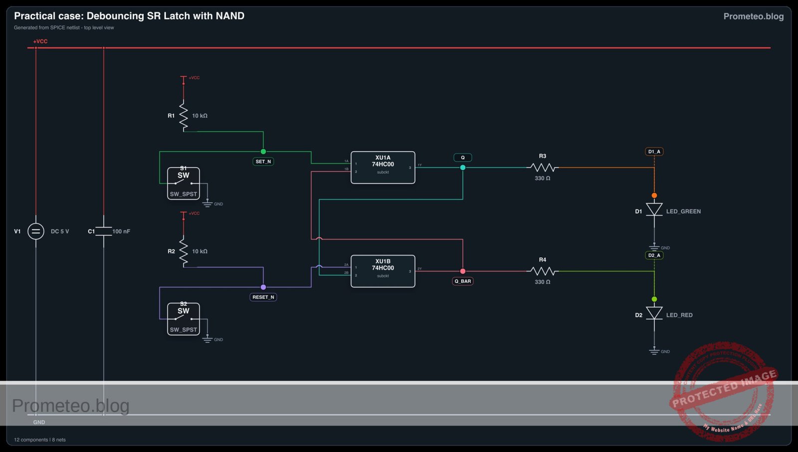
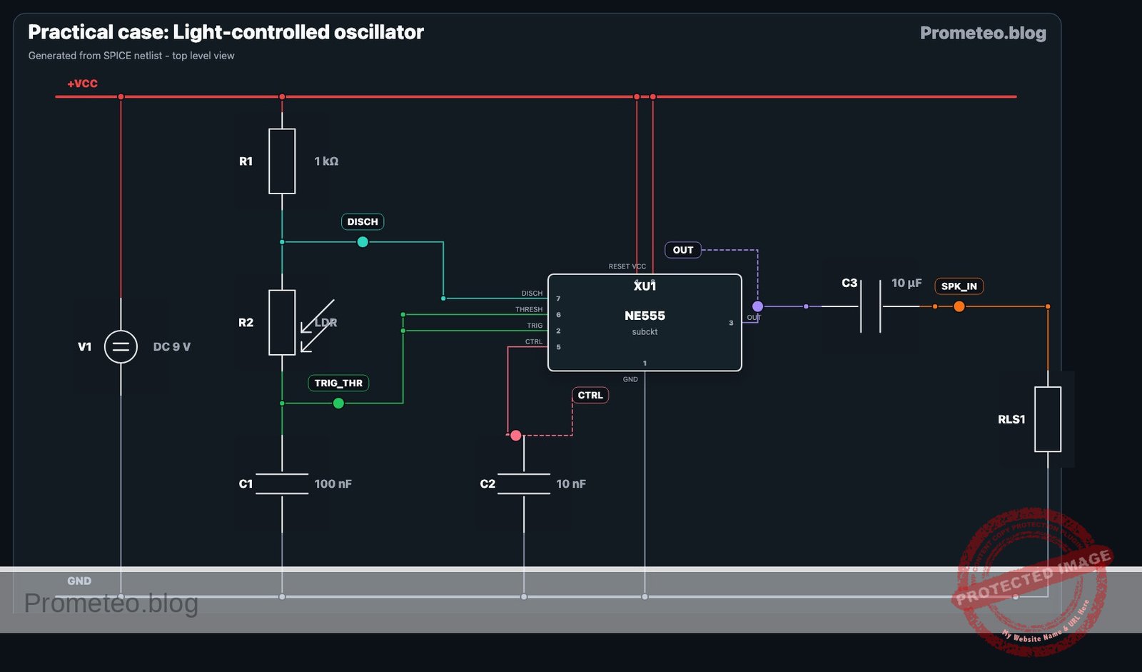
V1: 9 V DC supplyU1: NE555 timer IC, function: astable oscillatorR1: 1 kΩ resistor, function: fixed timing resistor limiting discharge currentR2: Photoresistor (LDR), function: variable timing resistor modulated by lightC1: 100 nF ceramic capacitor, function: primary timing oscillator capacitorC2: 10 nF ceramic capacitor, function: control voltage stabilization for U1C3: 10 µF electrolytic capacitor, function: AC coupling for the speakerLS1: Piezoelectric speaker, function: audio output
Wiring guide
V1: connects between nodeVCCand node0(GND).U1Pin 1 (GND): connects to node0.U1Pin 8 (VCC): connects to nodeVCC.U1Pin 4 (RESET): connects to nodeVCC.U1Pin 7 (DISCHARGE): connects to nodeDISCH.U1Pin 2 (TRIGGER): connects to nodeTRIG_THR.U1Pin 6 (THRESHOLD): connects to nodeTRIG_THR.U1Pin 5 (CONTROL): connects to nodeCTRL.U1Pin 3 (OUTPUT): connects to nodeOUT.R1: connects between nodeVCCand nodeDISCH.R2: connects between nodeDISCHand nodeTRIG_THR.C1: connects between nodeTRIG_THRand node0.C2: connects between nodeCTRLand node0.C3: connects between nodeOUT(positive terminal) and nodeSPK_IN(negative terminal).LS1: connects between nodeSPK_INand node0.
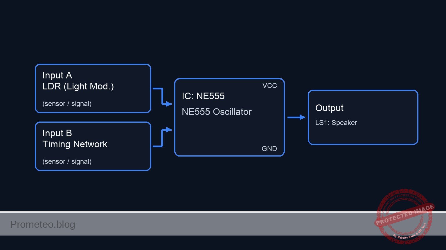
Conceptual block diagram
Schematic
Inputs / Timing Network                                        Processing                      Output / Load
=======================                                        ==========                      =============

[ VCC --> R1: 1 kΩ ] -----------------------(DISCH: Pin 7)----> [ U1: NE555 Timer ]
                                                               [                 ]
[ Node DISCH --> R2: LDR (Light Mod.) ] ---(TRIG_THR: Pins 2,6)[                 ]
                                                               [  (Oscillator)   ] --(OUT: Pin 3)--> [ C3: 10µF ] --(SPK_IN)--> [ LS1: Speaker ] --> GND
[ Node TRIG_THR --> C1: 100nF --> GND ] ---(Timing Ref)------> [                 ]
                                                               [                 ]
[ Node CTRL --> C2: 10nF --> GND ] --------(CTRL: Pin 5)-----> [                 ]
Electrical diagram
Measurements and tests
- LDR resistance: Before inserting the LDR into the circuit, measure its resistance with a digital multimeter. Record the value in absolute darkness (it should be very high, e.g., > 50 kΩ) and under direct flashlight illumination (it should drop significantly, e.g., < 1 kΩ).
- Capacitor voltage: Power the assembled circuit. Use an oscilloscope to probe the node
TRIG_THRwith respect to ground (node0). You should observe a continuous charge-discharge waveform (resembling a shark fin or triangle) oscillating exactly between 3 V and 6 V (which correspond to 1/3 and 2/3 of the 9 V supply). - Output frequency: Connect an oscilloscope or a frequency counter to node
OUTwith respect to ground. Shine a flashlight directly onto the LDR and observe the frequency rise rapidly. Cover the sensor with your hand to simulate darkness and watch the frequency fall.
SPICE netlist and simulation
Reference SPICE Netlist (ngspice) — excerptFull SPICE netlist (ngspice)
* Light-controlled oscillator (NE555 astable)
.width out=256

.op
.tran 10u 5m uic
.print tran V(TRIG_THR) V(OUT) V(VCC) V(SPK_IN)

* Power Supply
V1 VCC 0 DC 9

* 555 Timer IC Subcircuit Definition
.subckt NE555 1 2 3 4 5 6 7 8
* Pins: 1:GND 2:TRIG 3:OUT 4:RESET 5:CTRL 6:THR 7:DISCH 8:VCC
* Internal voltage divider
R1 8 5 5k
R2 5 N_TRIG_REF 5k
R3 N_TRIG_REF 1 5k

* Comparators using continuous tanh functions for robust convergence
B_S N_S 1 V=0.5 + 0.5*tanh(100 * (V(N_TRIG_REF) - V(2)))
* ... (truncated in public view) ...
Copy this content into a .cir file and run with ngspice.
* Light-controlled oscillator (NE555 astable)
.width out=256

.op
.tran 10u 5m uic
.print tran V(TRIG_THR) V(OUT) V(VCC) V(SPK_IN)

* Power Supply
V1 VCC 0 DC 9

* 555 Timer IC Subcircuit Definition
.subckt NE555 1 2 3 4 5 6 7 8
* Pins: 1:GND 2:TRIG 3:OUT 4:RESET 5:CTRL 6:THR 7:DISCH 8:VCC
* Internal voltage divider
R1 8 5 5k
R2 5 N_TRIG_REF 5k
R3 N_TRIG_REF 1 5k

* Comparators using continuous tanh functions for robust convergence
B_S N_S 1 V=0.5 + 0.5*tanh(100 * (V(N_TRIG_REF) - V(2)))
B_R N_R 1 V=0.5 + 0.5*tanh(100 * (V(6) - V(5)))
B_RESET N_RESET 1 V=0.5 + 0.5*tanh(100 * (0.7 - (V(4) - V(1))))

* SR Latch (Behavioral RC model ensuring smooth transitions)
B_INT N_INT 1 V=(V(N_RESET)<=0.5) * ( (V(N_S)>=0.5) + (V(N_S)<0.5) * (V(N_R)<=0.5) * V(N_INT_CAP) )
R_INT N_INT N_INT_CAP 100
C_INT N_INT_CAP 1 1n

* Output stage (Push-pull behavior)
B_OUT N_OUT 1 V=(V(N_INT_CAP)>0.5) * V(8)
R_OUT N_OUT 3 10

* Discharge stage (Open collector behavior)
B_DISCH 7 1 I=V(7) * ( (V(N_INT_CAP)<0.5)*0.1 + (V(N_INT_CAP)>=0.5)*1e-9 )
.ends

* Main Circuit
XU1 0 TRIG_THR OUT VCC CTRL TRIG_THR DISCH VCC NE555
R1 VCC DISCH 1k
R2 DISCH TRIG_THR 10k
C1 TRIG_THR 0 100n
C2 CTRL 0 10n
C3 OUT SPK_IN 10u
RLS1 SPK_IN 0 1k

.end
* --- GPT review (BOM/Wiring/SPICE) ---
* circuit_ok=true
* simulation_summary: The transient simulation shows the trigger/threshold voltage oscillating between approximately 3V (1/3 VCC) and 6V (2/3 VCC), and the output toggling between near 0V and near 9V. The AC-coupled speaker input (SPK_IN) correctly centers around 0V during operation.
* bom_vs_spice equivalences ignored:
*   - Photoresistor (LDR) R2 modeled as a fixed 10k resistor.
*   - Piezoelectric speaker LS1 modeled as a 1k resistor RLS1.
* overall_comment: The SPICE netlist accurately represents the light-controlled oscillator described in the BOM and wiring guide. The NE555 subcircuit functions correctly as an astable multivibrator, and the simulation results confirm the expected oscillation. The circuit is perfectly suitable as a didactic example.
* --------------------------------------
Simulation Results (Transient Analysis)

Show raw data table (631 rows)
Index   time            v(trig_thr)     v(out)          v(vcc)          v(spk_in)
0	1.000000e-07	8.901188e-06	0.000000e+00	9.000000e+00	0.000000e+00
1	1.014392e-07	2.067642e-05	8.910891e+00	9.000000e+00	8.910890e+00
2	1.043176e-07	4.422687e-05	8.910891e+00	9.000000e+00	8.910887e+00
3	1.100744e-07	9.132756e-05	8.910891e+00	9.000000e+00	8.910882e+00
4	1.215880e-07	1.855282e-04	8.910891e+00	9.000000e+00	8.910872e+00
5	1.446152e-07	3.739266e-04	8.910891e+00	9.000000e+00	8.910852e+00
6	1.906696e-07	7.507115e-04	8.910892e+00	9.000000e+00	8.910811e+00
7	2.827784e-07	1.504234e-03	8.910893e+00	9.000000e+00	8.910730e+00
8	4.361485e-07	2.758782e-03	8.910894e+00	9.000000e+00	8.910595e+00
9	6.136134e-07	4.210203e-03	8.910896e+00	9.000000e+00	8.910438e+00
10	8.824756e-07	6.408686e-03	8.910898e+00	9.000000e+00	8.910201e+00
11	1.315870e-06	9.951414e-03	8.910902e+00	9.000000e+00	8.909818e+00
12	2.182659e-06	1.703268e-02	8.910909e+00	9.000000e+00	8.909054e+00
13	3.916236e-06	3.117850e-02	8.910925e+00	9.000000e+00	8.907525e+00
14	7.383392e-06	5.940335e-02	8.910955e+00	9.000000e+00	8.904468e+00
15	1.000000e-05	8.064538e-02	8.910978e+00	9.000000e+00	8.902161e+00
16	1.069343e-05	8.626452e-02	8.910985e+00	9.000000e+00	8.901550e+00
17	1.208029e-05	9.749572e-02	8.910997e+00	9.000000e+00	8.900328e+00
18	1.485402e-05	1.199157e-01	8.911021e+00	9.000000e+00	8.897884e+00
19	2.040147e-05	1.645865e-01	8.911070e+00	9.000000e+00	8.892998e+00
20	3.040147e-05	2.445449e-01	8.911158e+00	9.000000e+00	8.884197e+00
21	4.040147e-05	3.237797e-01	8.911246e+00	9.000000e+00	8.875405e+00
22	5.040147e-05	4.022975e-01	8.911334e+00	9.000000e+00	8.866622e+00
23	6.040147e-05	4.801047e-01	8.911422e+00	9.000000e+00	8.857848e+00
... (607 more rows) ...
Reference SPICE netlist (ngspice)
* Light-controlled oscillator (NE555 astable)
.width out=256

.op
.tran 10u 5m uic
.print tran V(TRIG_THR) V(OUT) V(VCC) V(SPK_IN)

* Power Supply
V1 VCC 0 DC 9

* 555 Timer IC Subcircuit Definition
.subckt NE555 1 2 3 4 5 6 7 8
* Pins: 1:GND 2:TRIG 3:OUT 4:RESET 5:CTRL 6:THR 7:DISCH 8:VCC
* Internal voltage divider
R1 8 5 5k
R2 5 N_TRIG_REF 5k
R3 N_TRIG_REF 1 5k

* Comparators using continuous tanh functions for robust convergence
B_S N_S 1 V=0.5 + 0.5*tanh(100 * (V(N_TRIG_REF) - V(2)))
B_R N_R 1 V=0.5 + 0.5*tanh(100 * (V(6) - V(5)))
B_RESET N_RESET 1 V=0.5 + 0.5*tanh(100 * (0.7 - (V(4) - V(1))))

* SR Latch (Behavioral RC model ensuring smooth transitions)
B_INT N_INT 1 V=(V(N_RESET)=0.5) + (V(N_S)0.5) * V(8)
R_OUT N_OUT 3 10

* Discharge stage (Open collector behavior)
B_DISCH 7 1 I=V(7) * ( (V(N_INT_CAP)=0.5)*1e-9 )
.ends

* Main Circuit
XU1 0 TRIG_THR OUT VCC CTRL TRIG_THR DISCH VCC NE555
R1 VCC DISCH 1k
R2 DISCH TRIG_THR 10k
C1 TRIG_THR 0 100n
C2 CTRL 0 10n
C3 OUT SPK_IN 10u
RLS1 SPK_IN 0 1k

.end
* --- GPT review (BOM/Wiring/SPICE) ---
* circuit_ok=true
* simulation_summary: The transient simulation shows the trigger/threshold voltage oscillating between approximately 3V (1/3 VCC) and 6V (2/3 VCC), and the output toggling between near 0V and near 9V. The AC-coupled speaker input (SPK_IN) correctly centers around 0V during operation.
* bom_vs_spice equivalences ignored:
*   - Photoresistor (LDR) R2 modeled as a fixed 10k resistor.
*   - Piezoelectric speaker LS1 modeled as a 1k resistor RLS1.
* overall_comment: The SPICE netlist accurately represents the light-controlled oscillator described in the BOM and wiring guide. The NE555 subcircuit functions correctly as an astable multivibrator, and the simulation results confirm the expected oscillation. The circuit is perfectly suitable as a didactic example.
* --------------------------------------
Simulation Results (Transient Analysis)
Common mistakes and how to avoid them
- Swapping the positions of R1 and the LDR: If the LDR is placed between VCC and pin 7 (DISCHARGE), intense light will drop its resistance to almost zero. When the NE555 attempts to discharge the capacitor by grounding pin 7, it will create a near short-circuit from VCC to ground, potentially destroying the IC. Always keep a fixed safety resistor (R1) in the upper position.
- Choosing the wrong value for C1: If C1 is too large (like a 10 µF electrolytic capacitor), the oscillator will run at a sub-audio frequency, producing a series of clicks rather than a tone. Stick to the 10 nF to 100 nF range for audible results.
- Omitting the AC coupling capacitor (C3): Connecting the piezo speaker directly from the output pin to ground forces a constant DC offset through the speaker, which draws unnecessary power and can degrade the component over time. Always use an AC coupling capacitor to block the DC component.
Troubleshooting
- Symptom: The speaker emits a continuous clicking or ticking sound instead of a musical tone.
- Cause: The oscillation frequency is too low, likely below 20 Hz.
- Fix: Check the value of C1. Ensure it is a 100 nF ceramic capacitor (often marked 104) and not a much larger electrolytic capacitor. Also, ensure the LDR is not in total darkness.
- Symptom: No sound is produced, and the NE555 chip feels hot to the touch.
- Cause: A short circuit during the discharge cycle.
- Fix: Disconnect power immediately. Verify that R1 is a fixed 1 kΩ resistor and that the LDR is strictly placed between pins 7 and 6, NOT between VCC and pin 7.
- Symptom: A tone is heard, but the pitch barely changes when waving a hand over the sensor.
- Cause: The resistance swing of the LDR in current lighting conditions is too small, or ambient room light is too uniform.
- Fix: Test the circuit by shining a highly focused light source (like a smartphone flashlight) directly onto the LDR, then completely covering it with a dark cup. If the tone still doesn’t change much, verify that R2 is indeed an LDR and not a standard fixed resistor by mistake.
Possible improvements and extensions
- Manual tuning potentiometer: Add a 10 kΩ potentiometer in series with the LDR. This allows you to manually offset the total resistance, providing a way to tune the «base pitch» of the oscillator for different room lighting conditions.
- Inverse light response: Modify the configuration so that pitch decreases as light increases. This can be achieved by rewiring the timing section (keeping safety resistors in mind) or by using a secondary transistor to invert the LDR’s behavior over the control voltage (Pin 5) of the NE555 instead of the standard timing network.
More Practical Cases on Prometeo.blog
Find this product and/or books on this topic on Amazon
As an Amazon Associate, I earn from qualifying purchases. If you buy through this link, you help keep this project running.
Quick Quiz

Telecommunications Electronics Engineer and Computer Engineer (official degrees in Spain).