Level: Basic – Verify the frequency division relationship on the Q outputs of a binary counter relative to the clock.
Objective and use case
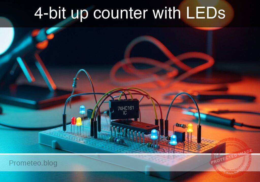
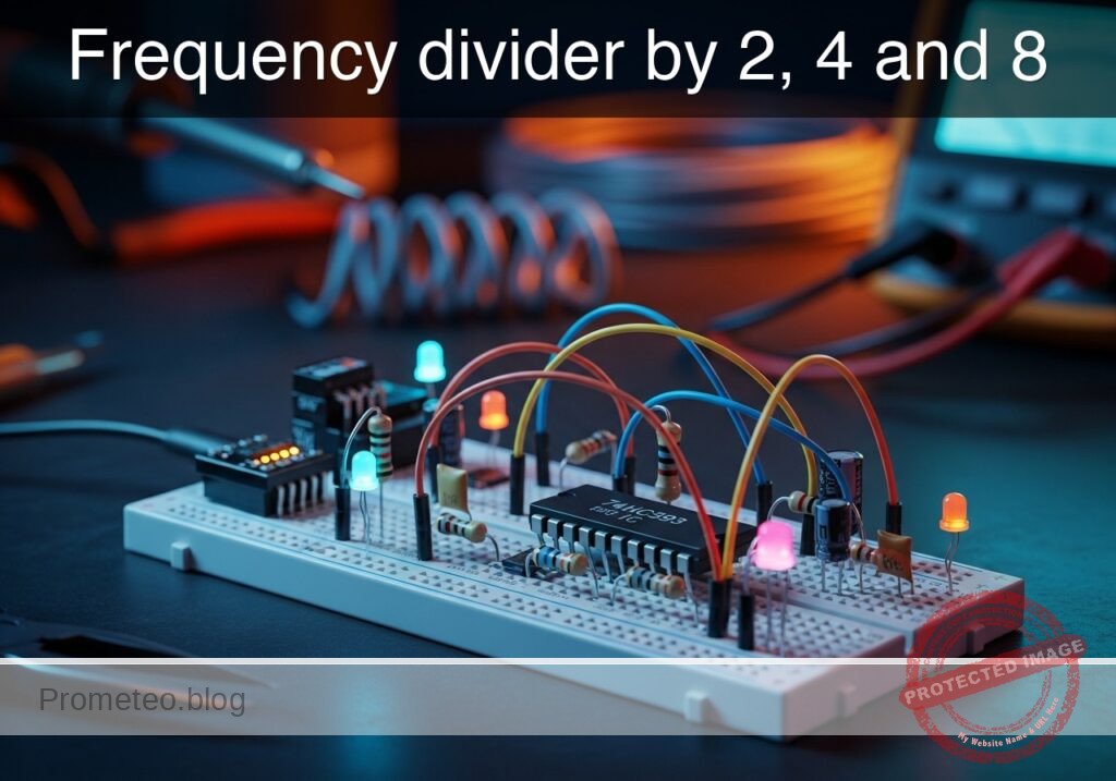
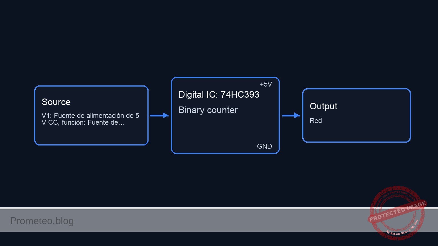
In this practical case, you will build a digital circuit using a 4-bit binary counter (74HC393) to divide an input clock signal frequency by factors of 2 (2^1), 4 (2^2), and 8 (2^3).
- Digital Clocks: Used to divide high-frequency crystal oscillator signals down to 1 Hz for keeping time (seconds).
- Audio Synthesis: Used to generate lower octaves from a base tone (frequency halving results in a tone one octave lower).
- Baud Rate Generation: Used in UART communication to derive specific data transmission speeds from a master system clock.
- Address Counters: Used to sequence through memory addresses in microcontrollers.
Expected outcome:
* Q0 Output: A square wave with a frequency exactly half of the input clock (f/2).
* Q1 Output: A square wave with a frequency one-quarter of the input clock (f/4).
* Q2 Output: A square wave with a frequency one-eighth of the input clock (f/8).
* Target Audience: Basic level students and hobbyists.
Materials
- V1: 5 V DC supply, function: Main power source.
- V_CLK: Pulse generator (0 V to 5 V, 1 kHz, 50% duty cycle), function: Input Clock signal.
- U1: 74HC393, function: Dual 4-bit Binary Counter.
- R1: 330 Ω resistor, function: Current limiting for LED D1.
- R2: 330 Ω resistor, function: Current limiting for LED D2.
- R3: 330 Ω resistor, function: Current limiting for LED D3.
- D1: Red LED, function: Visual indicator for Q0 (f/2).
- D2: Green LED, function: Visual indicator for Q1 (f/4).
- D3: Yellow LED, function: Visual indicator for Q2 (f/8).
- Scope: 4-Channel Oscilloscope, function: Waveform analysis.
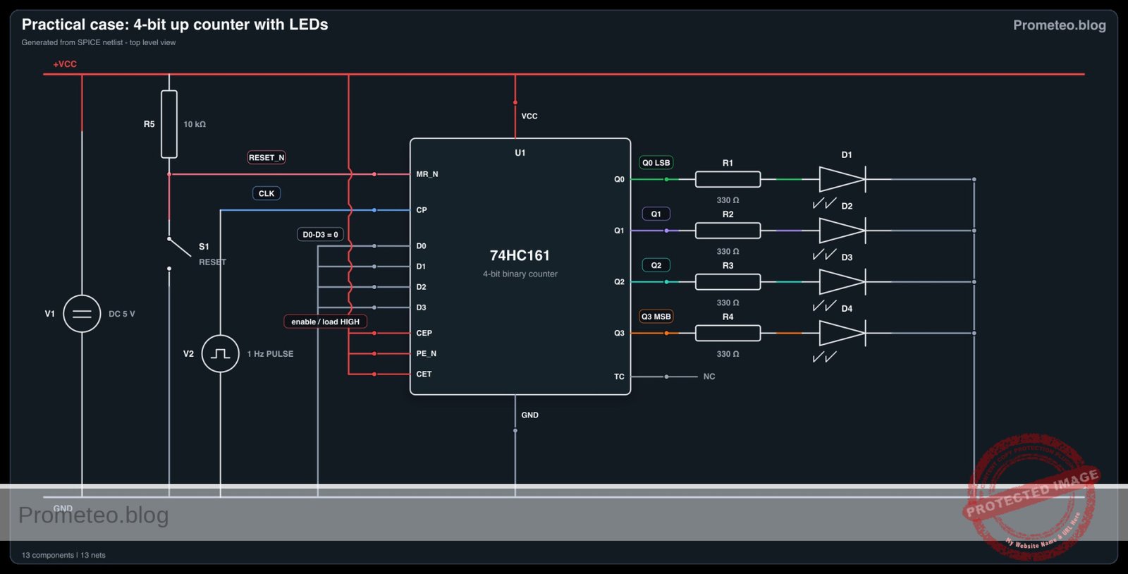
Pin-out of the IC used
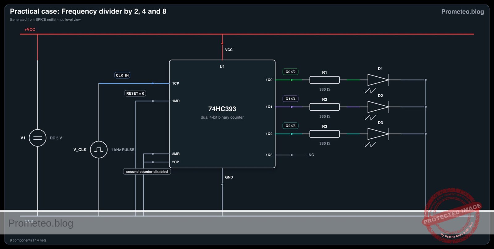
Selected Chip: 74HC393 (Dual 4-bit Binary Counter). We will use the first counter block (Side 1).
| Pin | Name | Logic function | Connection in this case |
|---|---|---|---|
| 1 | 1CP (CLK) | Clock Input (Falling edge trigger) | Connected to CLK_IN |
| 2 | 1MR | Master Reset (Active High) | Connected to 0 (GND) |
| 3 | 1Q0 | Output Bit 0 (Divide by 2) | Connected to Q0 |
| 4 | 1Q1 | Output Bit 1 (Divide by 4) | Connected to Q1 |
| 5 | 1Q2 | Output Bit 2 (Divide by 8) | Connected to Q2 |
| 7 | GND | Ground | Connected to 0 |
| 14 | VCC | Power Supply (+5 V) | Connected to VCC |
Wiring guide
- V1 connects between node
VCCand node0(GND). - U1 pin 14 connects to node
VCC. - U1 pin 7 connects to node
0(GND). - U1 pin 2 (Reset) connects to node
0(GND) to enable counting. - V_CLK connects between node
CLK_INand node0(GND). - U1 pin 1 connects to node
CLK_IN. - U1 pin 3 connects to node
Q0. - U1 pin 4 connects to node
Q1. - U1 pin 5 connects to node
Q2. - R1 connects between node
Q0and nodeLED_Q0. - D1 anode connects to
LED_Q0, cathode connects to0(GND). - R2 connects between node
Q1and nodeLED_Q1. - D2 anode connects to
LED_Q1, cathode connects to0(GND). - R3 connects between node
Q2and nodeLED_Q2. - D3 anode connects to
LED_Q2, cathode connects to0(GND).
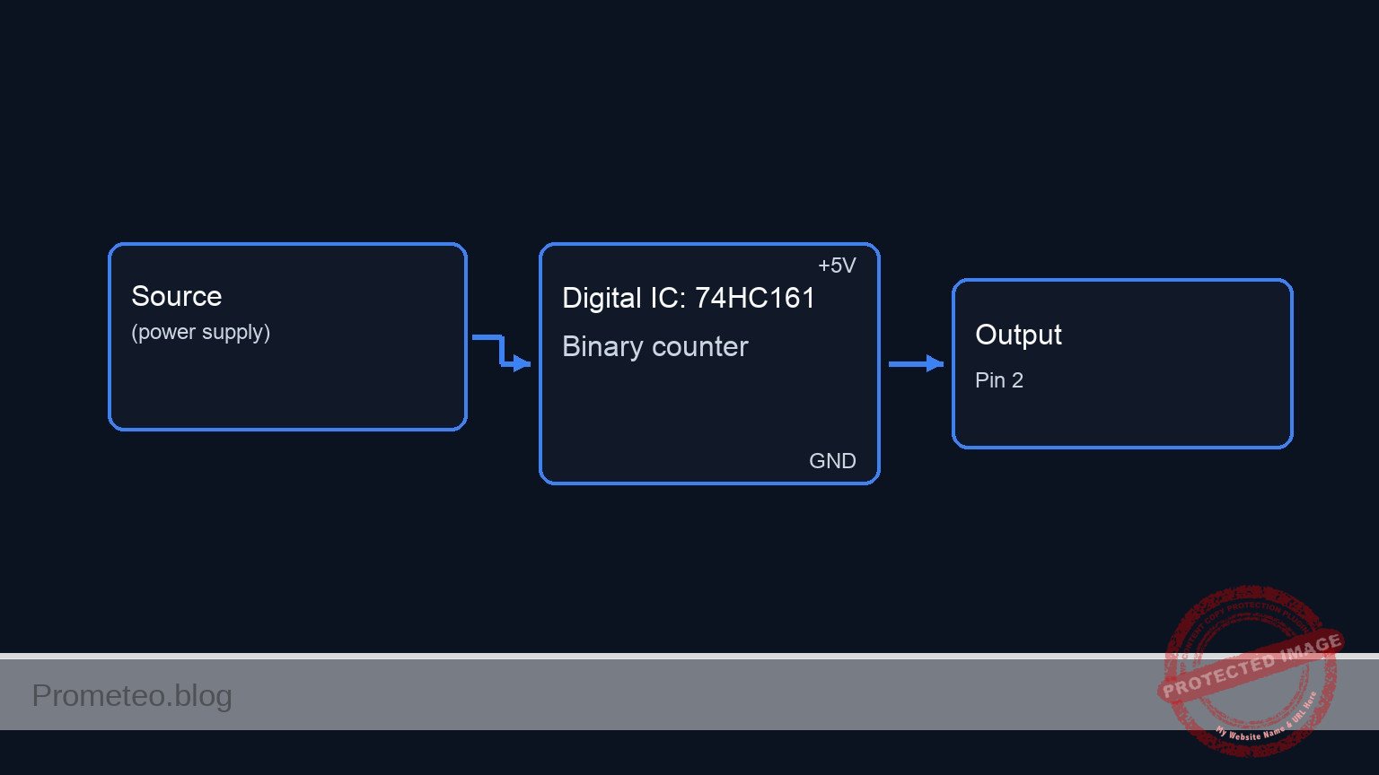
Conceptual block diagram
Schematic
INPUTS                                   PROCESSING                                     OUTPUTS / LOADS
(Left)                                    (Center)                                          (Right)

                                   +-----------------------+
                                   |                       |
 [ V_CLK: 1kHz ] --(Pin 1: CP)---> |                       | --(Pin 3: Q0)--> [ R1: 330 ] --> [ D1: Red ] --> GND
                                   |                       |       |
                                   |      U1: 74HC393      |       '--------(Scope Ch1: f/2)
                                   |      Dual 4-bit       |
                                   |      Bin Counter      |
 [ GND ] ---------(Pin 2: MR)--->  |                       | --(Pin 4: Q1)--> [ R2: 330 ] --> [ D2: Grn ] --> GND
             (Reset Disabled)      |   (Power: VCC=Pin 14, |       |
                                   |           GND=Pin 7)  |       '--------(Scope Ch2: f/4)
                                   |                       |
                                   |                       |
                                   |                       | --(Pin 5: Q2)--> [ R3: 330 ] --> [ D3: Yel ] --> GND
                                   |                       |       |
                                   +-----------------------+       '--------(Scope Ch3: f/8)
Electrical diagram
Measurements and tests
To validate the circuit, perform the following measurements using the 4-channel oscilloscope:
- Setup: Connect the Ground clip of all oscilloscope probes to node
0(GND). - Channel 1 (Input): Connect to
CLK_IN. Verify the frequency is 1 kHz. - Channel 2 (Q0): Connect to
Q0. Measure the frequency. It must be 500 Hz ($1kHz / 2$). - Channel 3 (Q1): Connect to
Q1. Measure the frequency. It must be 250 Hz ($1kHz / 4$). - Channel 4 (Q2): Connect to
Q2. Measure the frequency. It must be 125 Hz ($1kHz / 8$). - Visual Check: If you lower the input clock frequency to 10 Hz, you should see D1 blinking fastest, D2 slower, and D3 slowest.
SPICE netlist and simulation
Reference SPICE Netlist (ngspice) — excerptFull SPICE netlist (ngspice)
* Practical case: Frequency divider by 2, 4 and 8

.width out=256

* --- Models ---
* Generic LED Model
.model DLED D(IS=1e-14 N=2 RS=10 BV=5 IBV=10u CJO=10p)

* --- Power Supply ---
* V1: 5V Main Supply
V1 VCC 0 DC 5

* --- Input Signal ---
* V_CLK: 1kHz Pulse, 0V to 5V, 50% Duty Cycle
V_CLK CLK_IN 0 PULSE(0 5 0 1u 1u 0.5m 1m)

* --- Subcircuit: 74HC393 (Behavioral XSPICE) ---
* Dual 4-bit Binary Counter
* Implements Counter 1 logic using XSPICE primitives.
* Pinout (DIP-14): 1=1CP, 2=1MR, 3=1Q0, 4=1Q1, 5=1Q2, 6=1Q3, 7=GND
* ... (truncated in public view) ...
Copy this content into a .cir file and run with ngspice.
* Practical case: Frequency divider by 2, 4 and 8

.width out=256

* --- Models ---
* Generic LED Model
.model DLED D(IS=1e-14 N=2 RS=10 BV=5 IBV=10u CJO=10p)

* --- Power Supply ---
* V1: 5V Main Supply
V1 VCC 0 DC 5

* --- Input Signal ---
* V_CLK: 1kHz Pulse, 0V to 5V, 50% Duty Cycle
V_CLK CLK_IN 0 PULSE(0 5 0 1u 1u 0.5m 1m)

* --- Subcircuit: 74HC393 (Behavioral XSPICE) ---
* Dual 4-bit Binary Counter
* Implements Counter 1 logic using XSPICE primitives.
* Pinout (DIP-14): 1=1CP, 2=1MR, 3=1Q0, 4=1Q1, 5=1Q2, 6=1Q3, 7=GND
*                  8=2Q3, 9=2Q2, 10=2Q1, 11=2Q0, 12=2MR, 13=2CP, 14=VCC
.subckt 74HC393 1CP 1MR 1Q0 1Q1 1Q2 1Q3 GND 2Q3 2Q2 2Q1 2Q0 2MR 2CP VCC

    * ADC Bridge to read analog inputs (Clock and Reset)
    .model adc_mod adc_bridge(in_low=1.5 in_high=3.5)
    A_IN [1CP 1MR] [d_1cp d_1mr] adc_mod

    * ADC Bridge to read GND for Logic Low (used for SET inputs)
    A_GND [GND] [d_low] adc_mod

    * Logic Models
    .model inv_mod d_inverter(rise_delay=10n fall_delay=10n)
    .model dff_mod d_dff(clk_delay=10n rise_delay=10n fall_delay=10n)
    .model dac_mod dac_bridge(out_low=0.0 out_high=5.0)

    * --- Counter Logic (Side 1) ---
    * 74HC393 triggers on High-to-Low transition of CP.
    * XSPICE DFF triggers on Rising Edge. So we invert CP.
    A_INV1 d_1cp d_1cp_inv inv_mod

    * Stage 1 (Q0): Divider by 2
    * T-FF behavior: D = ~Q. Clock = ~CP. Reset = MR.
    * Port order: din clk set reset out nout
    A_DFF1 d_1q0_bar d_1cp_inv d_low d_1mr d_1q0 d_1q0_bar dff_mod

    * Stage 2 (Q1): Divider by 4
    * Ripples from Q0 Falling Edge.
    * Q0 Falling = ~Q0 Rising. Use d_1q0_bar as clock.
    A_DFF2 d_1q1_bar d_1q0_bar d_low d_1mr d_1q1 d_1q1_bar dff_mod

    * Stage 3 (Q2): Divider by 8
    * Ripples from Q1 Falling Edge. Use d_1q1_bar as clock.
    A_DFF3 d_1q2_bar d_1q1_bar d_low d_1mr d_1q2 d_1q2_bar dff_mod

    * Stage 4 (Q3): Divider by 16 (Not used externally but part of logic)
    A_DFF4 d_1q3_bar d_1q2_bar d_low d_1mr d_1q3 d_1q3_bar dff_mod

    * Drive Outputs
    A_OUT [d_1q0 d_1q1 d_1q2 d_1q3] [1Q0 1Q1 1Q2 1Q3] dac_mod

    * Side 2 is unused, inputs grounded in main circuit, outputs open.
.ends 74HC393

* --- Main Circuit Instances ---
* U1: 74HC393 Counter
* Pin connections based on Wiring Guide:
* 1(CLK_IN), 2(0/Reset), 3(Q0), 4(Q1), 5(Q2), 7(0/GND), 14(VCC)
* Unused outputs mapped to NC nodes. Unused inputs to 0.
* Subcircuit Pin Order: 1CP 1MR 1Q0 1Q1 1Q2 1Q3 GND 2Q3 2Q2 2Q1 2Q0 2MR 2CP VCC
XU1 CLK_IN 0 Q0 Q1 Q2 NC_1Q3 0 NC_2Q3 NC_2Q2 NC_2Q1 NC_2Q0 0 0 VCC 74HC393

* --- Output Paths (LEDs and Resistors) ---
* Path 1: Q0 -> R1 -> D1 (Red)
R1 Q0 LED_Q0 330
D1 LED_Q0 0 DLED

* Path 2: Q1 -> R2 -> D2 (Green)
R2 Q1 LED_Q1 330
D2 LED_Q1 0 DLED

* Path 3: Q2 -> R3 -> D3 (Yellow)
R3 Q2 LED_Q2 330
D3 LED_Q2 0 DLED

* --- Simulation & Output ---
.op
.tran 10u 20m
.print tran V(CLK_IN) V(Q0) V(Q1) V(Q2)

.end
* --- GPT review (BOM/Wiring/SPICE) ---
* circuit_ok=true
* simulation_summary: The simulation shows a clear binary counting sequence. CLK_IN is a 1kHz clock (period 1ms). Q0 toggles every 1ms (f/2, period 2ms). Q1 toggles every 2ms (f/4, period 4ms). Q2 toggles every 4ms (f/8, period 8ms). The outputs transition cleanly between 0V and 5V.
* bom_vs_spice equivalences ignored:
*   - LEDs (D1, D2, D3) are modeled using a generic diode model (DLED) with specific parameters.
*   - U1 (74HC393) is modeled as a behavioral subcircuit using XSPICE primitives (ADC/DAC bridges, DFFs) instead of a transistor-level model.
* overall_comment: The circuit is perfectly functional and accurately represents a 3-bit binary ripple counter (frequency divider). The behavioral model for the 74HC393 is correctly implemented with the necessary ADC/DAC bridges for XSPICE. The wiring matches the guide exactly, and the simulation results confirm the expected frequency division ratios (f/2, f/4, f/8). It is an excellent didactic example.
* --------------------------------------
Simulation Results (Transient Analysis)

Show raw data table (3323 rows)
Index   time            v(clk_in)       v(q0)           v(q1)           v(q2)
0	0.000000e+00	0.000000e+00	0.000000e+00	0.000000e+00	0.000000e+00
1	1.000000e-08	5.000000e-02	0.000000e+00	0.000000e+00	0.000000e+00
2	2.000000e-08	1.000000e-01	0.000000e+00	0.000000e+00	0.000000e+00
3	4.000000e-08	2.000000e-01	0.000000e+00	0.000000e+00	0.000000e+00
4	8.000000e-08	4.000000e-01	0.000000e+00	0.000000e+00	0.000000e+00
5	1.600000e-07	8.000000e-01	0.000000e+00	0.000000e+00	0.000000e+00
6	3.200000e-07	1.600000e+00	0.000000e+00	0.000000e+00	0.000000e+00
7	6.400000e-07	3.200000e+00	0.000000e+00	0.000000e+00	0.000000e+00
8	1.000000e-06	5.000000e+00	0.000000e+00	0.000000e+00	0.000000e+00
9	1.064000e-06	5.000000e+00	0.000000e+00	0.000000e+00	0.000000e+00
10	1.192000e-06	5.000000e+00	0.000000e+00	0.000000e+00	0.000000e+00
11	1.448000e-06	5.000000e+00	0.000000e+00	0.000000e+00	0.000000e+00
12	1.960000e-06	5.000000e+00	0.000000e+00	0.000000e+00	0.000000e+00
13	2.984000e-06	5.000000e+00	0.000000e+00	0.000000e+00	0.000000e+00
14	5.032000e-06	5.000000e+00	0.000000e+00	0.000000e+00	0.000000e+00
15	9.128000e-06	5.000000e+00	0.000000e+00	0.000000e+00	0.000000e+00
16	1.732000e-05	5.000000e+00	0.000000e+00	0.000000e+00	0.000000e+00
17	2.732000e-05	5.000000e+00	0.000000e+00	0.000000e+00	0.000000e+00
18	3.732000e-05	5.000000e+00	0.000000e+00	0.000000e+00	0.000000e+00
19	4.732000e-05	5.000000e+00	0.000000e+00	0.000000e+00	0.000000e+00
20	5.732000e-05	5.000000e+00	0.000000e+00	0.000000e+00	0.000000e+00
21	6.732000e-05	5.000000e+00	0.000000e+00	0.000000e+00	0.000000e+00
22	7.732000e-05	5.000000e+00	0.000000e+00	0.000000e+00	0.000000e+00
23	8.732000e-05	5.000000e+00	0.000000e+00	0.000000e+00	0.000000e+00
... (3299 more rows) ...
Common mistakes and how to avoid them
- Floating the Master Reset (MR) pin: Leaving pin 2 disconnected causes the counter to reset randomly due to noise. Solution: Always tie the MR pin to GND (Logic 0) for normal counting operation.
- Confusing Pin Numbers: The 74HC393 has two counters inside. Students often mix pins from Counter 1 and Counter 2. Solution: Strictly follow the datasheet and use pins 1, 2, 3, 4, 5, and 6 for the first counter only.
- Ignoring VCC/GND: Forgetting to power the chip leads to unpredictable output or no activity. Solution: Always connect Pin 14 to +5 V and Pin 7 to GND before testing.
Troubleshooting
- Symptom: No LEDs light up, and outputs remain at 0 V.
- Cause: Master Reset (Pin 2) might be connected to VCC instead of GND.
- Fix: Move connection of Pin 2 to GND.
- Symptom: LEDs are always on or flickering very dimly.
- Cause: Frequency is too high for the eye to see blinking (e.g., 1 kHz).
- Fix: Use the oscilloscope to verify the signal, or lower V_CLK frequency to < 10 Hz for visual confirmation.
- Symptom: Output frequency is unstable or erratic.
- Cause: Noisy power supply or lack of decoupling capacitor.
- Fix: Add a 100 nF capacitor across VCC and GND near the IC.
Possible improvements and extensions
- Divide by 16 and 256: Cascade the first counter into the second counter of the U1 chip (connect 1Q3 to 2CP) to achieve higher division ratios up to 256.
- Variable Audio Generator: Connect the outputs to a simple speaker driver and use a variable potentiometer on a 555 timer (as the clock) to hear how the pitch drops by octaves as you switch between Q0, Q1, and Q2.
More Practical Cases on Prometeo.blog
Find this product and/or books on this topic on Amazon
As an Amazon Associate, I earn from qualifying purchases. If you buy through this link, you help keep this project running.
Quick Quiz

Telecommunications Electronics Engineer and Computer Engineer (official degrees in Spain).