Level: Basic | Build a fail-safe alarm system using NAND logic to detect open windows.
Objective and use case
In this practical case, you will build a digital logic circuit that monitors two window sensors. The alarm will remain silent (LED OFF) only when both windows are securely closed. If either window is opened—or if a wire is cut—the alarm triggers (LED ON).
- Home Security: Monitoring multiple entry points (windows/doors) where all must be closed to secure the perimeter.
- Machine Safety: Ensuring all safety guards or maintenance hatches are closed before a machine can operate (or signaling a fault if opened).
- Fail-Safe Design: Demonstrating how active-high loops detect broken wires or open switches as alarm conditions.
Expected outcome:
* Safe State: When both switches (windows) are closed (Logic 1), the Output is 0 V (LED OFF).
* Alarm State: If Switch 1 OR Switch 2 is opened (Logic 0), the Output rises to ≈ 5 V (LED ON).
* Logic Verification: Confirmation of the NAND truth table behavior where Output is LOW only if all inputs are HIGH.
Target audience: Electronics students and hobbyists learning basic digital logic gates.
Materials
- V1: 5 V DC power supply, function: Main circuit power
- U1: 74HC00, function: Quad 2-input NAND gate IC
- SW1: SPST switch, function: Window 1 sensor (Closed = Window Closed)
- SW2: SPST switch, function: Window 2 sensor (Closed = Window Closed)
- R1: 10 kΩ resistor, function: Pull-down for SW1
- R2: 10 kΩ resistor, function: Pull-down for SW2
- R3: 330 Ω resistor, function: Current limiting for LED
- D1: Red LED, function: Alarm indicator
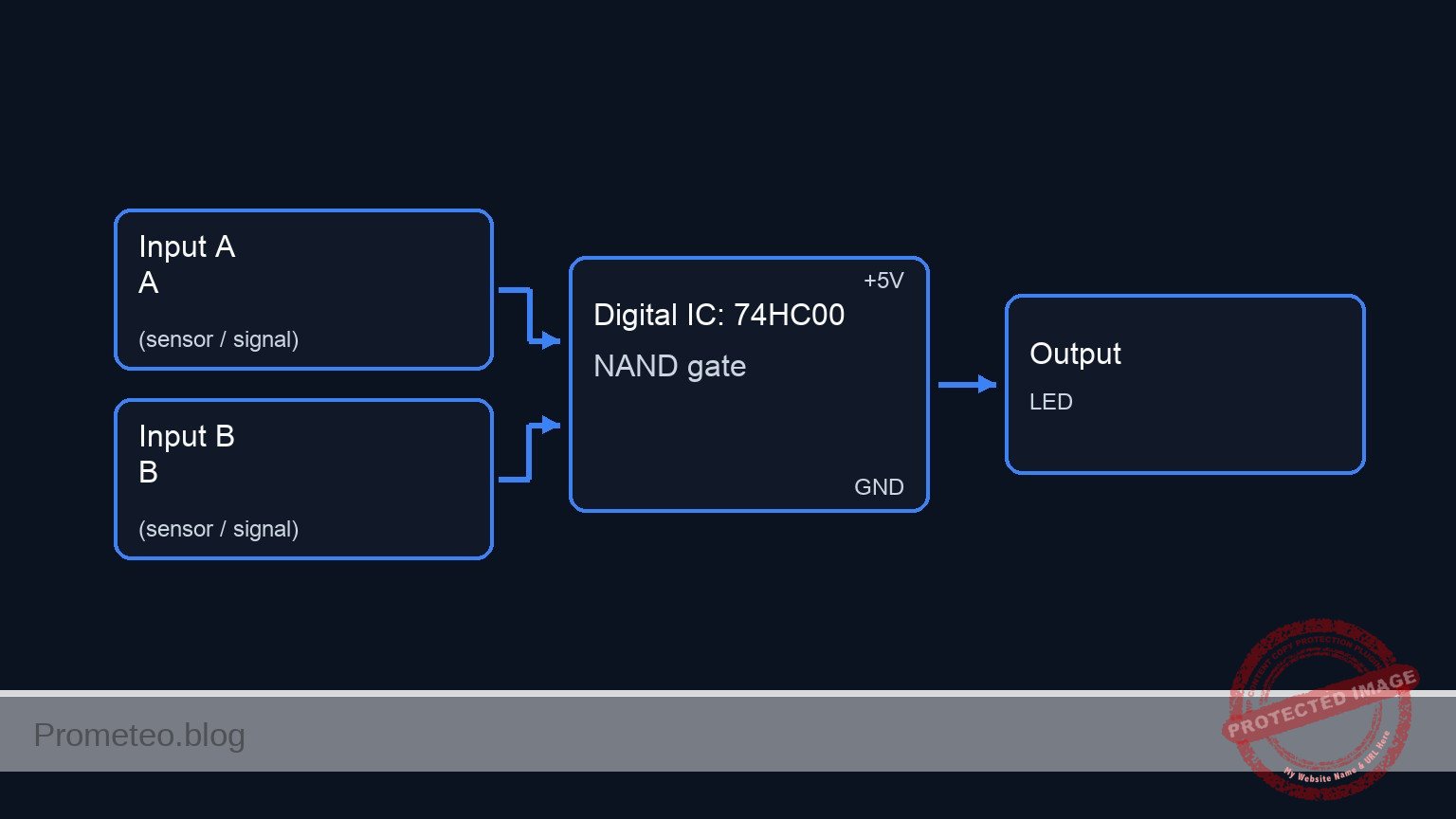
Pin-out of the IC used
Chip Selected: 74HC00 (Quad 2-Input NAND Gate)
| Pin | Name | Logic Function | Connection in this case |
|---|---|---|---|
| 1 | 1 A | Input A | Connected to Node SENS1 |
| 2 | 1B | Input B | Connected to Node SENS2 |
| 3 | 1Y | Output | Connected to Node ALARM_OUT |
| 7 | GND | Ground | Connected to Node 0 (GND) |
| 14 | VCC | Power Supply | Connected to Node VCC (5 V) |
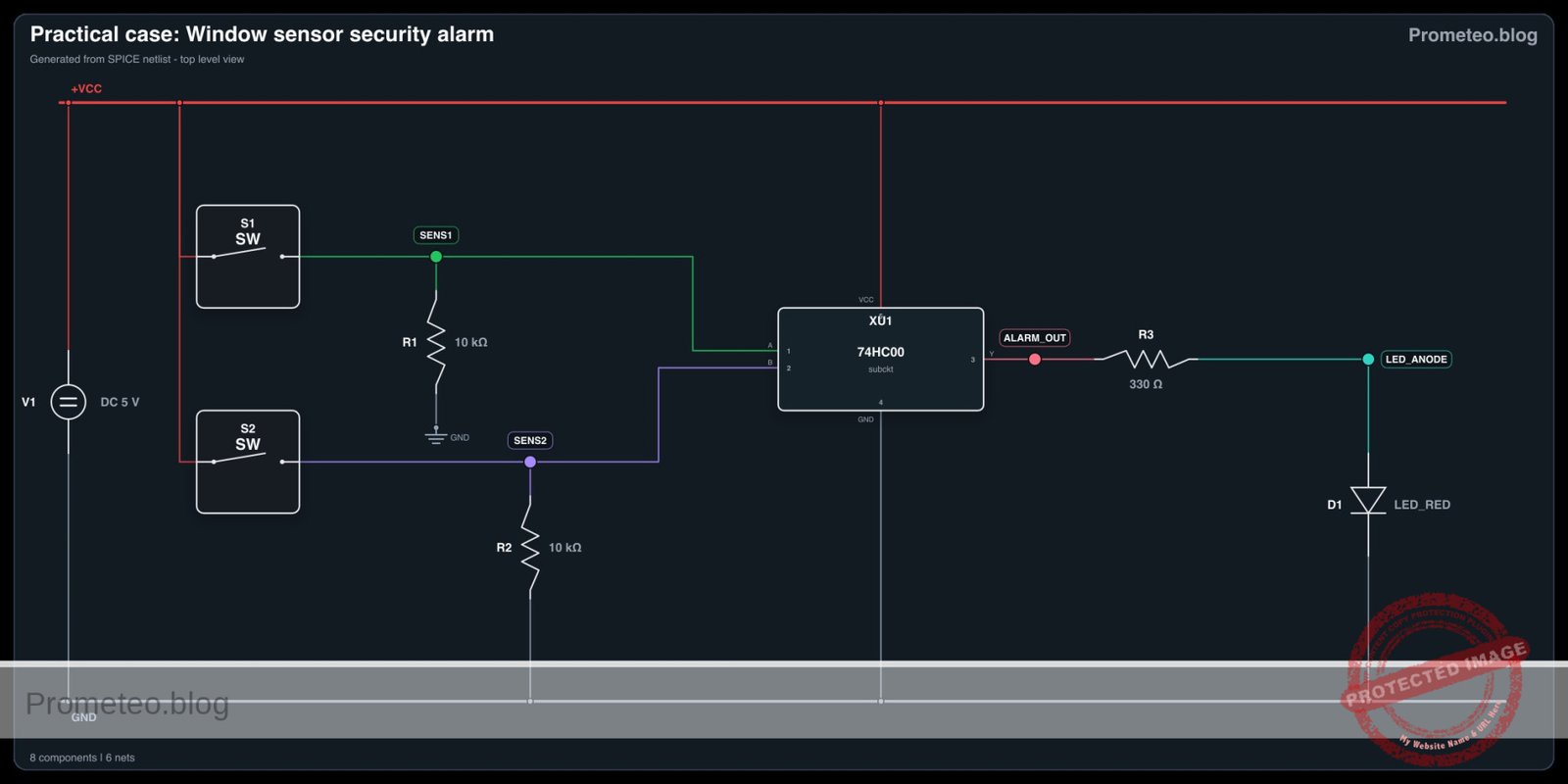
Wiring guide
This guide uses specific node names to help you visualize the connections on a breadboard.
- Power Rail: Connect
V1positive terminal to nodeVCCand negative terminal to node0. - IC Power: Connect U1 pin 14 to
VCCand U1 pin 7 to0. - Sensor 1: Connect
SW1betweenVCCand nodeSENS1. - Pull-down 1: Connect
R1betweenSENS1and0. - Sensor 2: Connect
SW2betweenVCCand nodeSENS2. - Pull-down 2: Connect
R2betweenSENS2and0. - Logic Input: Connect U1 pin 1 (1 A) to
SENS1and U1 pin 2 (1B) toSENS2. - Logic Output: Connect U1 pin 3 (1Y) to node
ALARM_OUT. - Indicator: Connect
R3betweenALARM_OUTand the Anode ofD1. - LED Ground: Connect the Cathode of
D1to node0.
Conceptual block diagram
Schematic
Title: Practical case: Window sensor security alarm

(Input Stage: Sensors)                  (Processing Stage: Logic)             (Output Stage: Alarm)

[ VCC ]
   |
[ SW1: Window 1 ]
   |
   +--(SENS1)-------+-----------------> [ U1: Pin 1 (Input A) ]
                    |                                         |
                 [ R1: 10k ]                                  v
                    |                                 [ U1: NAND Gate ] --(ALARM_OUT)--> [ R3: 330 Ω ] --> [ D1: LED ] --> GND
                 [ GND ]                                      ^
                                                              |
[ VCC ]             |                                         |
   |                |                                         |
[ SW2: Window 2 ]   |                                         |
   |                |                                         |
   +--(SENS2)-------+-----------------> [ U1: Pin 2 (Input B) ]
                    |
                 [ R2: 10k ]
                    |
                 [ GND ]
Electrical diagram
Truth table
The 74HC00 implements the NAND function. In this security context, Logic 1 represents a «Closed Window» (Safe), and Logic 0 represents an «Open Window» (Breach).
| Window 1 (SW1) | Window 2 (SW2) | Input A (Pin 1) | Input B (Pin 2) | Output Y (Pin 3) | LED State | Status |
|---|---|---|---|---|---|---|
| Closed | Closed | 1 (High) | 1 (High) | 0 (Low) | OFF | Secure |
| Open | Closed | 0 (Low) | 1 (High) | 1 (High) | ON | ALARM |
| Closed | Open | 1 (High) | 0 (Low) | 1 (High) | ON | ALARM |
| Open | Open | 0 (Low) | 0 (Low) | 1 (High) | ON | ALARM |
Measurements and tests
Follow these steps to validate your alarm system:
- Initial Power-Up: Ensure both switches (SW1, SW2) are closed. Turn on the 5 V supply. The LED
D1should be OFF. - Voltage Check (Secure): Use a multimeter to measure the voltage at node
ALARM_OUT. It should be close to 0 V (< 0.2 V). - Breach Test 1: Open SW1 while keeping SW2 closed. The LED should turn ON. Measure
ALARM_OUT; it should read close to 5 V. - Breach Test 2: Close SW1 and open SW2. The LED should turn ON.
- Total Breach: Open both switches. The LED should remain ON.
SPICE netlist and simulation
Reference SPICE Netlist (ngspice) — excerptFull SPICE netlist (ngspice)
* Practical case: Window sensor security alarm
.width out=256
* ngspice netlist

* --- Component Models ---
* Switch model for SW1 and SW2 (Sensors)
* Vt=2.5V: Switch closes when control voltage > 2.5V
* Ron=1m: Low resistance when closed
* Roff=100Meg: High resistance when open
.model SW_MOD SW(Vt=2.5 Ron=1m Roff=100Meg)

* LED model for D1
.model LED_RED D(IS=1e-22 RS=5 N=1.5 CJO=10p BV=5)

* --- Power Supply ---
* V1: 5 V DC power supply connected to VCC and 0 (GND)
V1 VCC 0 DC 5

* --- Window Sensor 1 ---
* Control source V_ACT1 simulates the physical action of opening/closing Window 1
* ... (truncated in public view) ...
Copy this content into a .cir file and run with ngspice.
* Practical case: Window sensor security alarm
.width out=256
* ngspice netlist

* --- Component Models ---
* Switch model for SW1 and SW2 (Sensors)
* Vt=2.5V: Switch closes when control voltage > 2.5V
* Ron=1m: Low resistance when closed
* Roff=100Meg: High resistance when open
.model SW_MOD SW(Vt=2.5 Ron=1m Roff=100Meg)

* LED model for D1
.model LED_RED D(IS=1e-22 RS=5 N=1.5 CJO=10p BV=5)

* --- Power Supply ---
* V1: 5 V DC power supply connected to VCC and 0 (GND)
V1 VCC 0 DC 5

* --- Window Sensor 1 ---
* Control source V_ACT1 simulates the physical action of opening/closing Window 1
* Logic: High (5V) = Window Closed, Low (0V) = Window Open
* Timing: Toggles every 100us (Period 200us)
V_ACT1 ACT1 0 PULSE(0 5 0 1u 1u 100u 200u)

* SW1: Connects VCC to SENS1 when window is closed
S1 VCC SENS1 ACT1 0 SW_MOD

* R1: Pull-down resistor for SENS1 (10k)
R1 SENS1 0 10k

* --- Window Sensor 2 ---
* Control source V_ACT2 simulates Window 2
* Timing: Toggles every 200us (Period 400us) to test all truth table combinations
V_ACT2 ACT2 0 PULSE(0 5 0 1u 1u 200u 400u)

* SW2: Connects VCC to SENS2 when window is closed
S2 VCC SENS2 ACT2 0 SW_MOD

* R2: Pull-down resistor for SENS2 (10k)
R2 SENS2 0 10k

* --- Logic IC: U1 (74HC00) ---
* Quad 2-input NAND gate. We instantiate one gate.
* Pin mapping according to wiring guide:
* Pin 1 (Input A) -> SENS1
* Pin 2 (Input B) -> SENS2
* Pin 3 (Output Y) -> ALARM_OUT
* Pin 7 -> GND (0), Pin 14 -> VCC
XU1 SENS1 SENS2 ALARM_OUT 0 VCC 74HC00_GATE

* Subcircuit for NAND Gate using robust continuous functions
.subckt 74HC00_GATE A B Y GND VCC
* Logic: Y = NAND(A, B) = NOT(A AND B)
* Implemented using sigmoid functions for convergence:
* 1 / (1 + exp(-k*(V-Vth))) acts as a smooth logical comparator.
* Vth = 2.5V, k = 20
B_NAND Y GND V = V(VCC) * (1 - ( (1/(1+exp(-20*(V(A)-2.5)))) * (1/(1+exp(-20*(V(B)-2.5)))) ))
.ends

* --- Alarm Output Indicator ---
* R3: Current limiting resistor (330 Ohm)
R3 ALARM_OUT LED_ANODE 330

* D1: Red LED connected to Ground
D1 LED_ANODE 0 LED_RED

* --- Simulation Commands ---
.op
* Transient analysis for 500us to capture all logic states
.tran 1u 500u

* Output configuration
* We print the Sensor inputs and the Alarm output
.print tran V(SENS1) V(SENS2) V(ALARM_OUT) V(LED_ANODE)

.end
Simulation Results (Transient Analysis)

Show raw data table (657 rows)
Index   time            v(sens1)        v(sens2)        v(alarm_out)    v(led_anode)
0	0.000000e+00	4.999500e-04	4.999500e-04	5.000000e+00	1.833072e+00
1	1.000000e-08	4.999500e-04	4.999500e-04	5.000000e+00	1.833072e+00
2	2.000000e-08	4.999500e-04	4.999500e-04	5.000000e+00	1.833072e+00
3	4.000000e-08	4.999500e-04	4.999500e-04	5.000000e+00	1.833072e+00
4	8.000000e-08	4.999500e-04	4.999500e-04	5.000000e+00	1.833072e+00
5	1.600000e-07	4.999500e-04	4.999500e-04	5.000000e+00	1.833072e+00
6	3.200000e-07	4.999500e-04	4.999500e-04	5.000000e+00	1.833072e+00
7	3.562500e-07	4.999500e-04	4.999500e-04	5.000000e+00	1.833072e+00
8	4.196875e-07	4.999500e-04	4.999500e-04	5.000000e+00	1.833072e+00
9	4.372461e-07	4.999500e-04	4.999500e-04	5.000000e+00	1.833072e+00
10	4.679736e-07	4.999500e-04	4.999500e-04	5.000000e+00	1.833072e+00
11	4.795524e-07	4.999500e-04	4.999500e-04	5.000000e+00	1.833072e+00
12	4.902290e-07	4.999500e-04	4.999500e-04	5.000000e+00	1.833072e+00
13	5.023412e-07	5.000000e+00	5.000000e+00	3.894872e-36	1.057689e+00
14	5.138120e-07	5.000000e+00	5.000000e+00	3.894872e-36	-7.61250e-02
15	5.160398e-07	5.000000e+00	5.000000e+00	3.894872e-36	-3.72798e-02
16	5.172425e-07	5.000000e+00	5.000000e+00	3.894872e-36	-2.57490e-02
17	5.188923e-07	5.000000e+00	5.000000e+00	3.894872e-36	-1.54585e-02
18	5.214063e-07	5.000000e+00	5.000000e+00	3.894872e-36	-6.97976e-03
19	5.238372e-07	5.000000e+00	5.000000e+00	3.894872e-36	-3.25627e-03
20	5.261078e-07	5.000000e+00	5.000000e+00	3.894872e-36	-1.60566e-03
21	5.281984e-07	5.000000e+00	5.000000e+00	3.894872e-36	-8.40881e-04
22	5.304310e-07	5.000000e+00	5.000000e+00	3.894872e-36	-4.20300e-04
23	5.328536e-07	5.000000e+00	5.000000e+00	3.894872e-36	-1.97001e-04
... (633 more rows) ...
Common mistakes and how to avoid them
- Floating Inputs: Forgetting R1 or R2 causes the inputs to «float» when switches are open, leading to erratic LED flickering. Solution: Always ensure inputs have a path to ground (via pull-down resistors) when the switch is open.
- LED Polarity: Connecting the LED backwards prevents it from lighting up even when the alarm is active. Solution: Ensure the longer leg (Anode) faces the resistor and IC output.
- Incorrect Switch Wiring: Placing the switch in parallel with the resistor instead of in series with the voltage source creates a short circuit. Solution: Follow the wiring guide: VCC -> Switch -> Node -> Resistor -> GND.
Troubleshooting
- Symptom: LED is always ON, even when switches are closed.
- Cause: One of the switches is not making contact, or an input wire is loose.
- Fix: Check continuity across SW1 and SW2; ensure pin 1 and pin 2 actually receive 5 V.
- Symptom: LED never turns ON.
- Cause: LED is reversed, IC is not powered, or R3 is too high.
- Fix: Check pin 14 for 5 V. Reverse the LED. Verify R3 is 330 Ω, not 330 kΩ.
- Symptom: Logic works reversed (LED ON when safe, OFF when open).
- Cause: You may be using an AND gate (74HC08) instead of NAND, or your switch/resistor logic is inverted (Pull-ups instead of Pull-downs).
- Fix: Verify the chip number is 74HC00.
Possible improvements and extensions
- Audible Alarm: Connect the base of an NPN transistor to
ALARM_OUTto drive a 5 V active buzzer, adding sound to the light. - Latching Alarm: Use the remaining gates in the 74HC00 to build an SR Latch. This would keep the alarm sounding even if the burglar closes the window immediately after entering.
More Practical Cases on Prometeo.blog
Find this product and/or books on this topic on Amazon
As an Amazon Associate, I earn from qualifying purchases. If you buy through this link, you help keep this project running.
Quick Quiz

Telecommunications Electronics Engineer and Computer Engineer (official degrees in Spain).