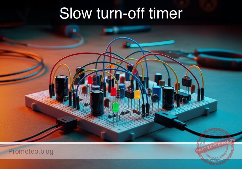
Level: Basic — Construct a circuit that fades an LED out slowly using capacitor discharge.
Objective and use case
In this practical case, you will build an analog timer circuit using an NPN transistor and a capacitor. When a push button is released, the LED will not turn off immediately; instead, it will dim gradually until it extinguishes.
- Interior car lighting: mimics the effect of dome lights fading out after the door is closed.
- Safety lighting: provides temporary illumination in hallways or stairwells after a switch is turned off.
- Debouncing simulation: demonstrates how capacitors smooth out sudden signal changes.
- Visualizing RC time constants: allows direct observation of electrical charge storage and decay.
Expected outcome:
* Immediate ON: When the button is pressed, the LED lights up instantly at full brightness.
* Delayed OFF: Upon releasing the button, the LED remains lit and fades out over a period of 2 to 5 seconds.
* Voltage Decay: If measured with a multimeter, the voltage at the capacitor decreases exponentially.
* Visual Feedback: The LED brightness directly correlates to the remaining charge in the capacitor.
* Target audience: Students and hobbyists understanding the relationship between capacitors and transistors.
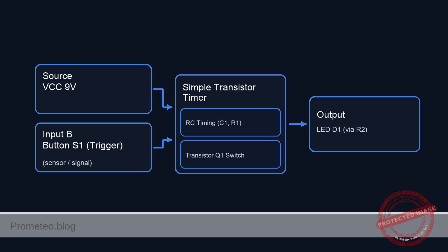
Materials
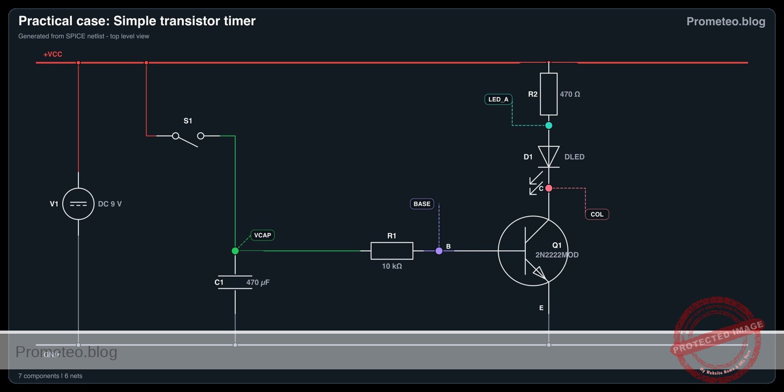
- V1: 9 V DC supply, function: main power source
- S1: Momentary push button (Normally Open), function: trigger mechanism
- R1: 100 Ω resistor, function: switch current protection (limits inrush current to capacitor)
- R2: 22 kΩ resistor, function: base current limiting and timing control
- R3: 470 Ω resistor, function: LED current limiting
- C1: 1000 µF electrolytic capacitor, function: charge storage (timing tank)
- Q1: 2N2222 (or BC547) NPN transistor, function: current switch/amplifier
- D1: Red LED, function: visual output indicator
Wiring guide
Use the following node connections to assemble the circuit on a breadboard.
-
Power Nodes:
- VCC: Positive rail (9 V).
- 0: Ground rail (0 V).
-
Switch and Capacitor Network (Nodes: VCC, V_STORE, 0):
- S1 connects between VCC and an intermediate node (internal to switch assembly).
- R1 connects between the switch output and V_STORE. (When S1 is pressed, V_STORE charges to ~9 V).
- C1 connects between V_STORE (positive leg) and 0 (negative leg).
-
Transistor Control (Nodes: V_STORE, V_BASE, 0):
- R2 connects between V_STORE and V_BASE.
- Q1 (Base) connects to V_BASE.
- Q1 (Emitter) connects to 0.
-
Output Stage (Nodes: VCC, V_COLL):
- R3 connects between VCC and the anode of D1.
- D1 (Cathode) connects to V_COLL.
- Q1 (Collector) connects to V_COLL.
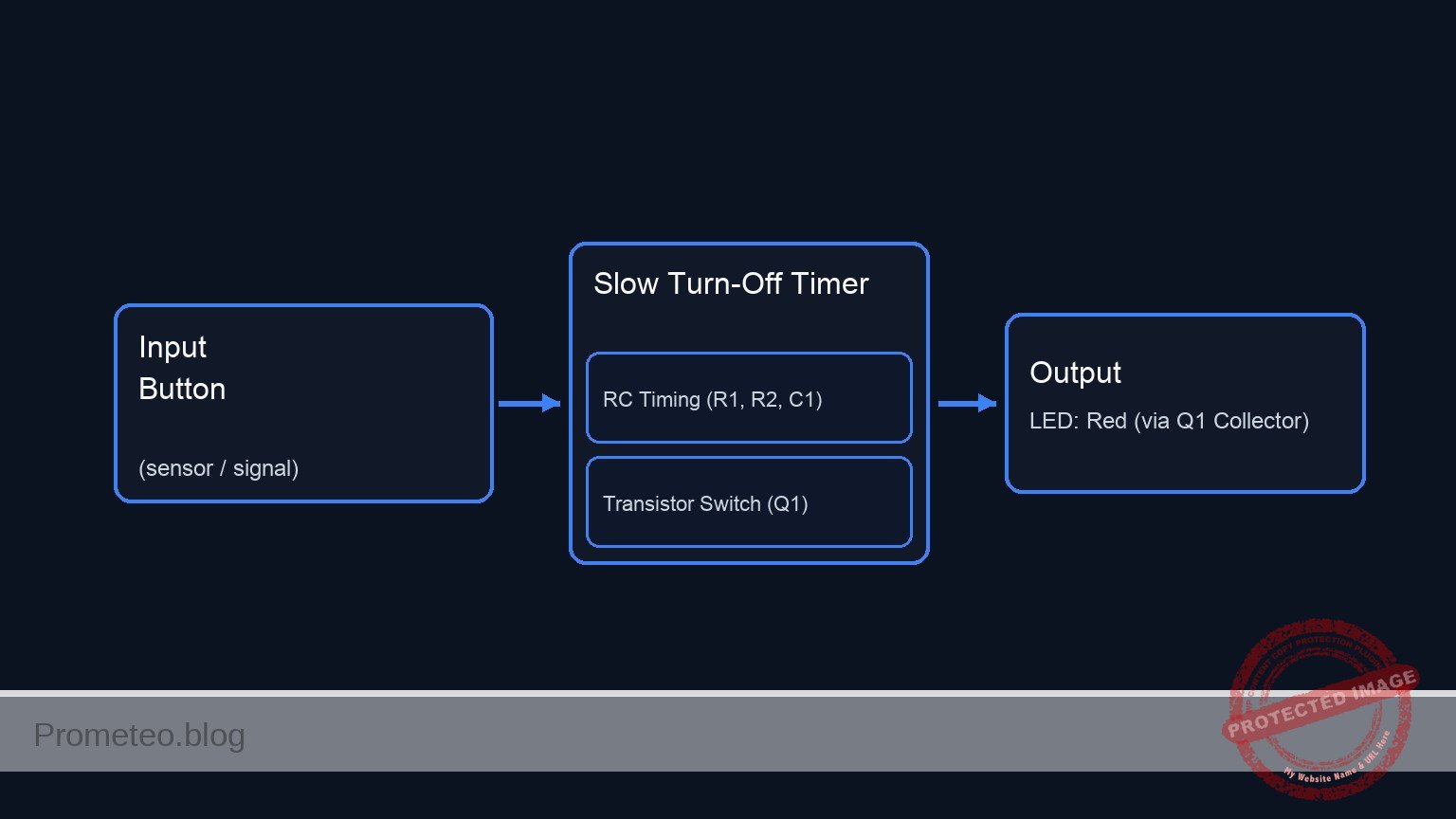
Conceptual block diagram
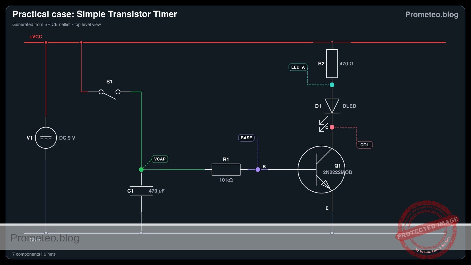
Schematic
+-------------------------------------------------------------------------+
|                       SLOW TURN-OFF TIMER DIAGRAM                       |
+-------------------------------------------------------------------------+

1. TIMING & CONTROL LOOP (Charges C1, drives Transistor Base)
---------------------------------------------------------------------------

VCC (9 V) --> [ S1: Button ] --> [ R1: 100 ] --(V_STORE)--> [ R2: 22k ] --> [ Q1:Base ]
                                                  |
                                                  v
                                            [ C1: 1000u ]
                                                  |
                                                  v
                                                 GND


2. OUTPUT LOAD LOOP (Powering the LED)
---------------------------------------------------------------------------

VCC (9 V) --> [ R3: 470 ] --> [ LED: Red ] --> [ Q1:Collector ]
                                                     |
                                                     v
                                              (Current Flow)
                                                     v
                                              [ Q1:Emitter ] --> GND
Electrical diagram
Measurements and tests
To validate the circuit operation, perform the following steps:
- Charging phase: Press and hold S1. Measure the voltage at V_STORE relative to Ground. It should rise rapidly to approximately 9 V. The LED D1 should be fully lit.
- Base activation: While holding S1, measure the voltage at V_BASE. It should differ from V_STORE due to the drop across R2, stabilizing around 0.7 V – 0.8 V (the Base-Emitter saturation voltage).
- Discharge phase: Release S1. Observe D1. It should not turn off instantly. Instead, it should fade.
- Time measurement: Use a stopwatch to measure the time from the moment S1 is released until the LED is completely dark. With a 1000 µF capacitor and 22 kΩ resistor, this should take several seconds.
- Voltage tracking: Connect a multimeter to V_STORE immediately after releasing the button. Watch the voltage drop. The LED usually turns off when V_STORE drops below the threshold required to maintain sufficient base current through R2 (roughly when V_STORE approaches 1.5 V – 2 V).
SPICE netlist and simulation
Reference SPICE Netlist (ngspice) — excerptFull SPICE netlist (ngspice)
* Practical case: Slow turn-off timer
.width out=256

* --- Models ---
* Standard NPN Transistor Model
.model 2N2222 NPN(IS=1E-14 VAF=100 BF=200 IKF=0.3 XTB=1.5 BR=3 CJC=8E-12 CJE=25E-12 TR=46.91E-9 TF=411.1E-12 ITF=0.6 VTF=1.7 XTF=3 RB=10 RC=1 RE=1)
* Generic Red LED Model (Vf approx 1.8V-2V)
.model DLED D(IS=1e-22 RS=10 N=1.5 CJO=50p)
* Switch Model for Push Button
.model SW_BTN SW(Vt=2.5 Ron=0.1 Roff=100M)

* --- Power Supply ---
V1 VCC 0 DC 9

* --- Input / Trigger Mechanism ---
* S1: Push Button. Modeled as a voltage-controlled switch connecting VCC to SW_OUT.
* V_BTN_ACT: Simulates the user pressing the button.
* Pulse starts at 1s, holds for 2s (simulating a solid press), then releases.
V_BTN_ACT CTRL 0 PULSE(0 5 1 0.1 0.1 2 100)
S1 VCC SW_OUT CTRL 0 SW_BTN
* ... (truncated in public view) ...
Copy this content into a .cir file and run with ngspice.
* Practical case: Slow turn-off timer
.width out=256

* --- Models ---
* Standard NPN Transistor Model
.model 2N2222 NPN(IS=1E-14 VAF=100 BF=200 IKF=0.3 XTB=1.5 BR=3 CJC=8E-12 CJE=25E-12 TR=46.91E-9 TF=411.1E-12 ITF=0.6 VTF=1.7 XTF=3 RB=10 RC=1 RE=1)
* Generic Red LED Model (Vf approx 1.8V-2V)
.model DLED D(IS=1e-22 RS=10 N=1.5 CJO=50p)
* Switch Model for Push Button
.model SW_BTN SW(Vt=2.5 Ron=0.1 Roff=100M)

* --- Power Supply ---
V1 VCC 0 DC 9

* --- Input / Trigger Mechanism ---
* S1: Push Button. Modeled as a voltage-controlled switch connecting VCC to SW_OUT.
* V_BTN_ACT: Simulates the user pressing the button.
* Pulse starts at 1s, holds for 2s (simulating a solid press), then releases.
V_BTN_ACT CTRL 0 PULSE(0 5 1 0.1 0.1 2 100)
S1 VCC SW_OUT CTRL 0 SW_BTN

* --- Switch Current Protection & Charging ---
* R1 limits inrush current to C1 when S1 is closed.
R1 SW_OUT V_STORE 100

* --- Timing Tank ---
* C1 charges when S1 is closed and discharges through R2/Q1 when open.
C1 V_STORE 0 1000u

* --- Transistor Control ---
* R2 provides base current and sets the discharge timing constant (Tau = R2*C1 approx 22s).
R2 V_STORE V_BASE 22k

* --- Transistor Switch ---
* Q1 NPN Transistor (2N2222)
* Collector: V_COLL, Base: V_BASE, Emitter: 0 (GND)
Q1 V_COLL V_BASE 0 2N2222

* --- Output Stage ---
* R3 limits current through the LED.
R3 VCC LED_ANODE 470
* D1 Red LED. Anode at LED_ANODE, Cathode at V_COLL.
D1 LED_ANODE V_COLL DLED

* --- Simulation Commands ---
.op
* Transient analysis for 60 seconds to capture the slow decay (RC ~ 22s).
.tran 0.1s 60s

* --- Output Directives ---
* Printing Capacitor Voltage (Timing) and Collector Voltage (Output State)
.print tran V(V_STORE) V(V_COLL) V(LED_ANODE) V(SW_OUT)
Simulation Results (Transient Analysis)

Show raw data table (640 rows)
Index   time            v(v_store)      v(v_coll)       v(led_anode)    v(sw_out)
0	0.000000e+00	8.962619e+00	1.066236e-01	2.056192e+00	8.999963e+00
1	1.000000e-03	8.962619e+00	1.066236e-01	2.056192e+00	8.999963e+00
2	2.000000e-03	8.962619e+00	1.066236e-01	2.056192e+00	8.999963e+00
3	4.000000e-03	8.962619e+00	1.066236e-01	2.056192e+00	8.999963e+00
4	8.000000e-03	8.962619e+00	1.066236e-01	2.056192e+00	8.999963e+00
5	1.600000e-02	8.962619e+00	1.066236e-01	2.056192e+00	8.999963e+00
6	3.200000e-02	8.962619e+00	1.066236e-01	2.056192e+00	8.999963e+00
7	6.400000e-02	8.962619e+00	1.066236e-01	2.056192e+00	8.999963e+00
8	1.280000e-01	8.962619e+00	1.066236e-01	2.056192e+00	8.999963e+00
9	2.280000e-01	8.962619e+00	1.066236e-01	2.056192e+00	8.999963e+00
10	3.280000e-01	8.962619e+00	1.066236e-01	2.056192e+00	8.999963e+00
11	4.280000e-01	8.962619e+00	1.066236e-01	2.056192e+00	8.999963e+00
12	5.280000e-01	8.962619e+00	1.066236e-01	2.056192e+00	8.999963e+00
13	6.280000e-01	8.962619e+00	1.066236e-01	2.056192e+00	8.999963e+00
14	7.280000e-01	8.962619e+00	1.066236e-01	2.056192e+00	8.999963e+00
15	8.280000e-01	8.962619e+00	1.066236e-01	2.056192e+00	8.999963e+00
16	9.280000e-01	8.962619e+00	1.066236e-01	2.056192e+00	8.999963e+00
17	1.000000e+00	8.962619e+00	1.066236e-01	2.056192e+00	8.999963e+00
18	1.010000e+00	8.962619e+00	1.066236e-01	2.056192e+00	8.999963e+00
19	1.026000e+00	8.962619e+00	1.066236e-01	2.056192e+00	8.999963e+00
20	1.030750e+00	8.962619e+00	1.066236e-01	2.056192e+00	8.999963e+00
21	1.039062e+00	8.962619e+00	1.066236e-01	2.056192e+00	8.999963e+00
22	1.041363e+00	8.962619e+00	1.066236e-01	2.056192e+00	8.999963e+00
23	1.045390e+00	8.962619e+00	1.066236e-01	2.056192e+00	8.999963e+00
... (616 more rows) ...
Common mistakes and how to avoid them
- Capacitor polarity reversed: Electrolytic capacitors have a specific polarity. Connecting the negative stripe to the positive voltage can cause the component to heat up or pop. Solution: Ensure the leg marked with a stripe (negative) connects to Ground.
- R2 value too low: If R2 is very small (e.g., 1 kΩ), the capacitor will discharge into the transistor base very quickly, resulting in no visible fading effect. Solution: Use a high resistance value (10 kΩ–47 kΩ) to slow down the discharge.
- Omitting R1: Connecting the switch directly to a large capacitor creates a massive current spike (spark) when pressed. Solution: Always use a small resistor (100 Ω) in series with the switch to protect the contacts.
Troubleshooting
- LED turns off instantly (no fade):
- Cause: Capacitor C1 is missing, disconnected, or the value is too small (e.g., 100 nF instead of 1000 µF).
- Fix: Verify C1 is correctly seated and is at least 470 µF.
- LED stays on permanently:
- Cause: The switch S1 might be the wrong type (Latching instead of Momentary) or there is a short circuit bypassing the transistor.
- Fix: Ensure the button releases physically and check wiring around the Collector-Emitter.
- LED is very dim even when button is pressed:
- Cause: R2 (Base resistor) is too high (limiting base current too much) or R3 (LED resistor) is too high.
- Fix: Check that R2 is roughly 22 kΩ and R3 is roughly 470 Ω.
Possible improvements and extensions
- Variable Timing: Replace R2 with a 100 kΩ potentiometer in series with a 1 kΩ resistor. This allows you to adjust the fade-out duration manually.
- Darlington Pair: Replace Q1 with a Darlington transistor (or two NPNs connected in Darlington configuration). This offers a much higher current gain, allowing you to use a much larger R2 (e.g., 1 MΩ), resulting in extremely long timer durations (minutes) with the same capacitor.
More Practical Cases on Prometeo.blog
Find this product and/or books on this topic on Amazon
As an Amazon Associate, I earn from qualifying purchases. If you buy through this link, you help keep this project running.
Quick Quiz

Telecommunications Electronics Engineer and Computer Engineer (official degrees in Spain).