Level: Basic – Understand the logic of a NOT gate (inverter) by observing opposite input and output states via light indicators.
Objective and use case
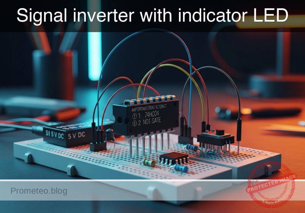
In this practical case, you will build a digital logic circuit using a 74HC04 Hex Inverter IC. The circuit will demonstrate the fundamental inversion function where a HIGH input signal results in a LOW output signal, visually confirmed by two LEDs operating in alternate states.
Why it is useful:
* Safety Interlocks: Used in machinery to ensure a system stops (logic LOW) when a sensor is activated (logic HIGH).
* Status Indicators: Allows creating «Standby» lights that turn ON only when the main power switch is OFF.
* Logic Level Adaptation: Essential for interfacing active-high sensors with active-low microcontroller inputs.
* Signal Conditioning: Cleans up noisy digital signals and ensures distinct logic levels.
Expected outcome:
* Input LED (Green): Turns ON when the switch is pressed (Logic 1).
* Output LED (Red): Turns OFF when the switch is pressed (Logic 0).
* Inverse Relationship: When the switch is released (Logic 0), the Red LED turns ON.
* Voltage Levels: Input at 0V $\rightarrow$ Output $\approx$ 5V; Input at 5V $\rightarrow$ Output $\approx$ 0V.
Target audience: Students and hobbyists (Level: Basic).
Materials
- V1: 5 V DC supply (battery or regulated power supply)
- S1: SPST toggle or tactile switch, function: Input signal generator
- U1: 74HC04 (Hex Inverter IC), function: Logic inversion
- R1: 10 kΩ resistor, function: Pull-down resistor for input VA
- R2: 330 Ω resistor, function: Current limiting for input LED (D1)
- R3: 330 Ω resistor, function: Current limiting for output LED (D2)
- D1: Green LED, function: Input state indicator (Active High)
- D2: Red LED, function: Output state indicator (Active High)
Pin-out of the IC used
Chip Selected: 74HC04 (Hex Inverter)
| Pin | Name | Logic function | Connection in this case |
|---|---|---|---|
| 1 | 1A | Input | Connected to Switch S1 and Pull-down R1 |
| 2 | 1Y | Output | Connected to Output LED (D2) via R3 |
| 7 | GND | Ground | Connected to Power Supply Negative (0V) |
| 14 | VCC | Power | Connected to Power Supply Positive (5V) |
Note: Pins 3, 4, 5, 6, 8, 9, 10, 11, 12, and 13 are unused in this single-gate demonstration. In a permanent circuit, unused inputs on CMOS chips should be tied to GND.
Wiring guide
- VCC: Connect positive terminal of V1, Pin 14 of U1, and one side of S1.
- 0 (GND): Connect negative terminal of V1, Pin 7 of U1, one side of R1, cathode of D1, and cathode of D2.
- VA (Input Node): Connect the other side of S1, the other side of R1, Pin 1 of U1, and one side of R2.
- Input Indicator: Connect the other side of R2 to the anode of D1.
- VOUT (Output Node): Connect Pin 2 of U1 to one side of R3.
- Output Indicator: Connect the other side of R3 to the anode of D2.
Conceptual block diagram

Schematic
[ INPUT GENERATION ]               [ LOGIC & MONITORING ]               [ OUTPUT STAGE ]

    [ VCC ] -> [ Switch S1 ] --+
                               |
                               V
                           (Node VA) --(Pin 1)--> [ U1: 74HC04 ] --(Pin 2)--> [ R3: 330 ] -> [ D2: Red ] -> GND
                               |                  (Hex Inverter)
                               |
    [ GND ] <- [ R1: 10k ] <---+
                               |
                               +----(Monitor)---> [ R2: 330 ] --> [ D1: Green ] -> GND
Truth table
The 74HC04 contains six independent NOT gates. We are using one.
| Input (VA) | Switch State | Output (VOUT) | Green LED (D1) | Red LED (D2) |
|---|---|---|---|---|
| 0 (Low) | Open | 1 (High) | OFF | ON |
| 1 (High) | Closed | 0 (Low) | ON | OFF |
Measurements and tests
To validate the circuit, perform the following steps using a multimeter and visual observation:
-
Default State Check:
- Ensure S1 is open (not pressed).
- Measure voltage at VA relative to GND. It should be 0V.
- Measure voltage at VOUT relative to GND. It should be close to 5V.
- Visual: Red LED (D2) is ON; Green LED (D1) is OFF.
-
Active State Check:
- Close (press) S1.
- Measure voltage at VA. It should be close to 5V.
- Measure voltage at VOUT. It should be close to 0V.
- Visual: Red LED (D2) turns OFF; Green LED (D1) turns ON.
-
Transition Threshold (Optional):
- If using a variable voltage source instead of S1, slowly increase voltage at VA. The output state will flip when the input crosses approximately half of VCC (approx. 2.5V for 74HC series).
SPICE netlist and simulation
Reference SPICE Netlist (ngspice) — excerptFull SPICE netlist (ngspice)
* Practical case: Signal inverter with indicator LED

* --- Power Supply ---
V1 VCC 0 DC 5

* --- Input Signal Generator (Switch S1) ---
* S1 connects VCC to VA (Input Node) when pressed.
* R1 pulls VA to Ground when S1 is open.
* V_S1_ACT simulates the user pressing the button (Active High).
* Pulse timing: Wait 10u, Press for 100u, Repeat every 200u.
V_S1_ACT S_ACT 0 PULSE(0 5 10u 1u 1u 100u 200u)
S1 VCC VA S_ACT 0 SW_IDEAL

* --- Input Circuit Components ---
R1 VA 0 10k
R2 VA N_D1_A 330
D1 N_D1_A 0 LED_GREEN

* --- Logic Inverter (U1: 74HC04) ---
* Wiring: Pin1=VA, Pin2=VOUT, Pin7=GND, Pin14=VCC
* Implemented as a behavioral subcircuit to match pinout
XU1 VA VOUT 0 VCC 74HC04_1G

* --- Output Circuit Components ---
R3 VOUT N_D2_A 330
D2 N_D2_A 0 LED_RED

* --- Models ---
* Voltage Controlled Switch Model
.model SW_IDEAL SW(Vt=2.5 Ron=1 Roff=10Meg)
* ... (truncated in public view) ...
Copy this content into a .cir file and run with ngspice.
* Practical case: Signal inverter with indicator LED

* --- Power Supply ---
V1 VCC 0 DC 5

* --- Input Signal Generator (Switch S1) ---
* S1 connects VCC to VA (Input Node) when pressed.
* R1 pulls VA to Ground when S1 is open.
* V_S1_ACT simulates the user pressing the button (Active High).
* Pulse timing: Wait 10u, Press for 100u, Repeat every 200u.
V_S1_ACT S_ACT 0 PULSE(0 5 10u 1u 1u 100u 200u)
S1 VCC VA S_ACT 0 SW_IDEAL

* --- Input Circuit Components ---
R1 VA 0 10k
R2 VA N_D1_A 330
D1 N_D1_A 0 LED_GREEN

* --- Logic Inverter (U1: 74HC04) ---
* Wiring: Pin1=VA, Pin2=VOUT, Pin7=GND, Pin14=VCC
* Implemented as a behavioral subcircuit to match pinout
XU1 VA VOUT 0 VCC 74HC04_1G

* --- Output Circuit Components ---
R3 VOUT N_D2_A 330
D2 N_D2_A 0 LED_RED

* --- Models ---
* Voltage Controlled Switch Model
.model SW_IDEAL SW(Vt=2.5 Ron=1 Roff=10Meg)

* LED Models (Generic)
.model LED_GREEN D(IS=1e-22 RS=5 N=1.5 CJO=50p)
.model LED_RED D(IS=1e-22 RS=5 N=1.5 CJO=50p)

* --- Subcircuits ---
* 74HC04 Hex Inverter (Single Gate Representation)
* Pins: 1=Input, 2=Output, 7=GND, 14=VCC
.subckt 74HC04_1G 1 2 7 14
* Behavioral source implementing Inverter Logic: Vout = NOT(Vin)
* Uses sigmoid function for convergence: 1 / (1 + exp(k*(Vin - Vth)))
* Multiplied by V(14) to track supply voltage
B1 2 7 V = V(14) * (1 / (1 + exp(50 * (V(1) - 2.5))))
.ends

* --- Analysis Directives ---
* Transient analysis for 500us to capture pulse cycles
.tran 1u 500u

* Output data for plotting/logging
.print tran V(VA) V(VOUT) V(N_D1_A) V(N_D2_A)

.op
.end
Simulation Results (Transient Analysis)

Show raw data table (1334 rows)
Index   time            v(va)           v(vout)         v(n_d1_a)
0	0.000000e+00	4.995005e-03	5.000000e+00	4.995005e-03
1	1.000000e-08	4.995005e-03	5.000000e+00	4.995005e-03
2	2.000000e-08	4.995005e-03	5.000000e+00	4.995005e-03
3	4.000000e-08	4.995005e-03	5.000000e+00	4.995005e-03
4	8.000000e-08	4.995005e-03	5.000000e+00	4.995005e-03
5	1.600000e-07	4.995005e-03	5.000000e+00	4.995005e-03
6	3.200000e-07	4.995005e-03	5.000000e+00	4.995005e-03
7	6.400000e-07	4.995005e-03	5.000000e+00	4.995005e-03
8	1.280000e-06	4.995005e-03	5.000000e+00	4.995005e-03
9	2.280000e-06	4.995005e-03	5.000000e+00	4.995005e-03
10	3.280000e-06	4.995005e-03	5.000000e+00	4.995005e-03
11	4.280000e-06	4.995005e-03	5.000000e+00	4.995005e-03
12	5.280000e-06	4.995005e-03	5.000000e+00	4.995005e-03
13	6.280000e-06	4.995005e-03	5.000000e+00	4.995005e-03
14	7.280000e-06	4.995005e-03	5.000000e+00	4.995005e-03
15	8.280000e-06	4.995005e-03	5.000000e+00	4.995005e-03
16	9.280000e-06	4.995005e-03	5.000000e+00	4.995005e-03
17	1.000000e-05	4.995005e-03	5.000000e+00	4.995005e-03
18	1.010000e-05	4.995005e-03	5.000000e+00	4.995005e-03
19	1.026000e-05	4.995005e-03	5.000000e+00	4.995005e-03
20	1.030750e-05	4.995005e-03	5.000000e+00	4.995005e-03
21	1.039062e-05	4.995005e-03	5.000000e+00	4.995005e-03
22	1.041363e-05	4.995005e-03	5.000000e+00	4.995005e-03
23	1.045390e-05	4.995005e-03	5.000000e+00	4.995005e-03
... (1310 more rows) ...
Common mistakes and how to avoid them
- Floating Inputs:
- Error: Omitting the pull-down resistor (R1). The input floats when the switch is open, causing the output LED to flicker or oscillate due to electromagnetic noise.
- Solution: Always ensure the input has a defined path to GND (via R1) when the switch is open.
- Missing Current Limiting Resistors:
- Error: Connecting LEDs directly to the IC output or VCC without R2 or R3.
- Solution: Always use series resistors (330 Ω to 1 kΩ) to prevent burning out the LED or damaging the 74HC04 output stage.
- Confusing Pin Numbering:
- Error: Wiring the IC upside down or counting pins from the wrong side.
- Solution: Identify the notch/dot on the package. Pin 1 is to the left of the notch when the notch faces up.
Troubleshooting
- Both LEDs remain OFF:
- Cause: Power supply disconnected or IC inserted backwards.
- Fix: Check VCC (Pin 14) and GND (Pin 7) connections. Ensure 5V is present.
- Output LED (Red) never turns OFF:
- Cause: The input VA is not reaching Logic High (5V) effectively, or the IC is damaged.
- Fix: Check the continuity of Switch S1. Measure voltage at Pin 1 while pressing the switch.
- Output LED (Red) is dim:
- Cause: Resistor R3 is too high in value, or the supply voltage is too low.
- Fix: Verify R3 is 330 Ω. Check if V1 is actually 5V.
Possible improvements and extensions
- Buffer Circuit: Connect the output of the first inverter (Pin 2) into the input of a second inverter (Pin 3). The output of the second inverter (Pin 4) will now match the original input state, acting as a non-inverting buffer.
- Square Wave Oscillator: Use three NOT gates in a ring loop (Logic Ring Oscillator) to create a circuit that blinks the LEDs automatically without a switch.
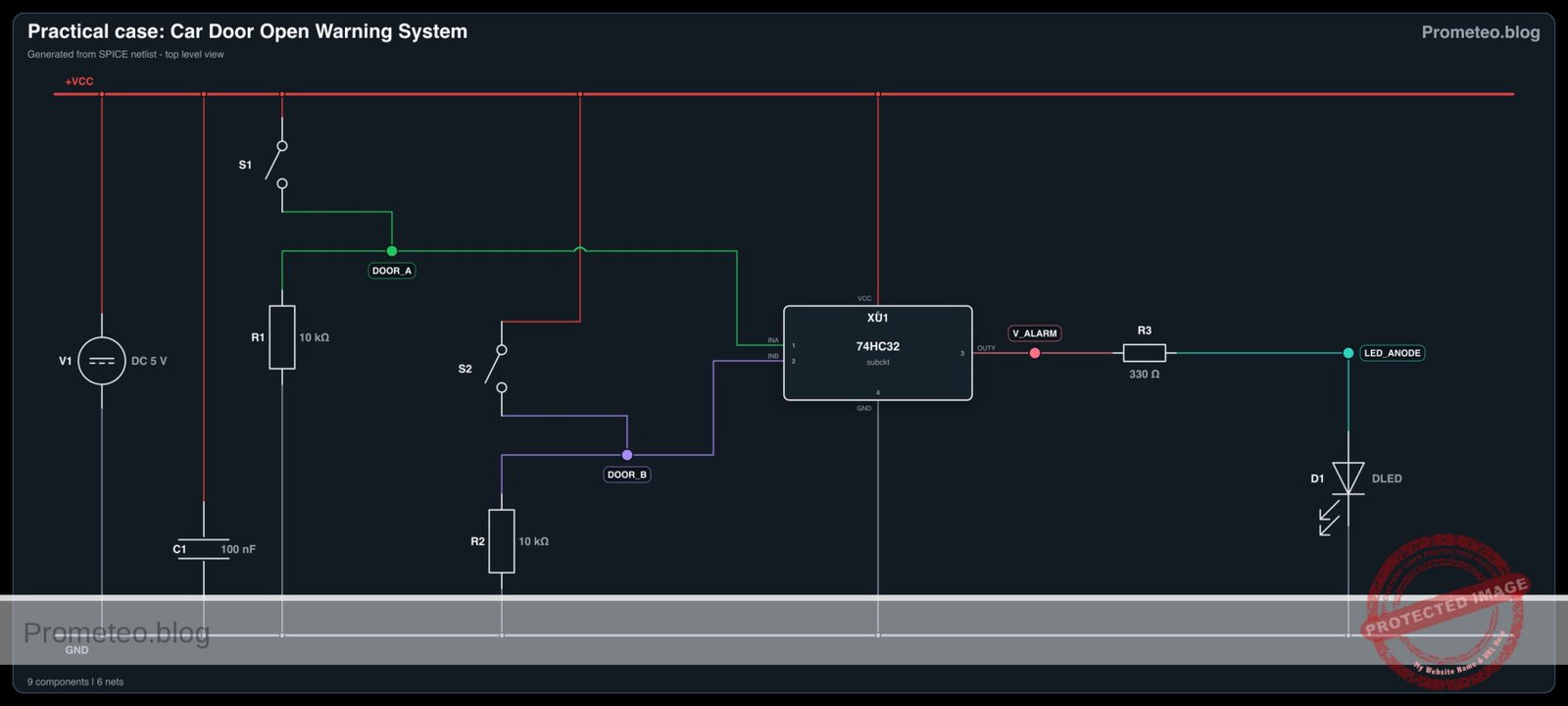
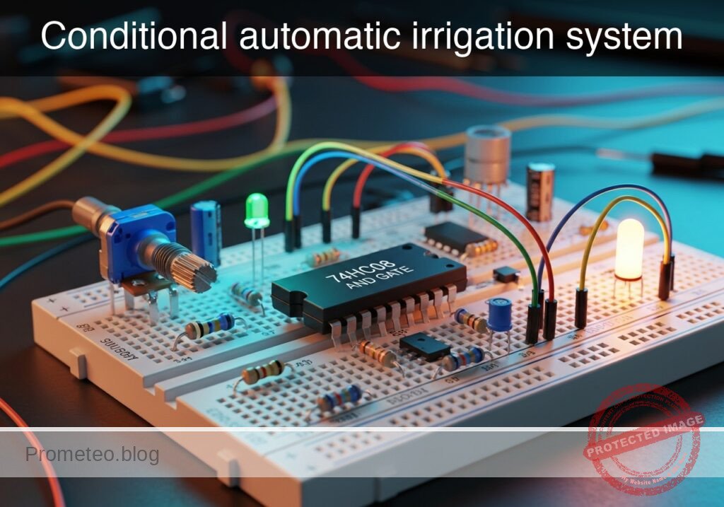
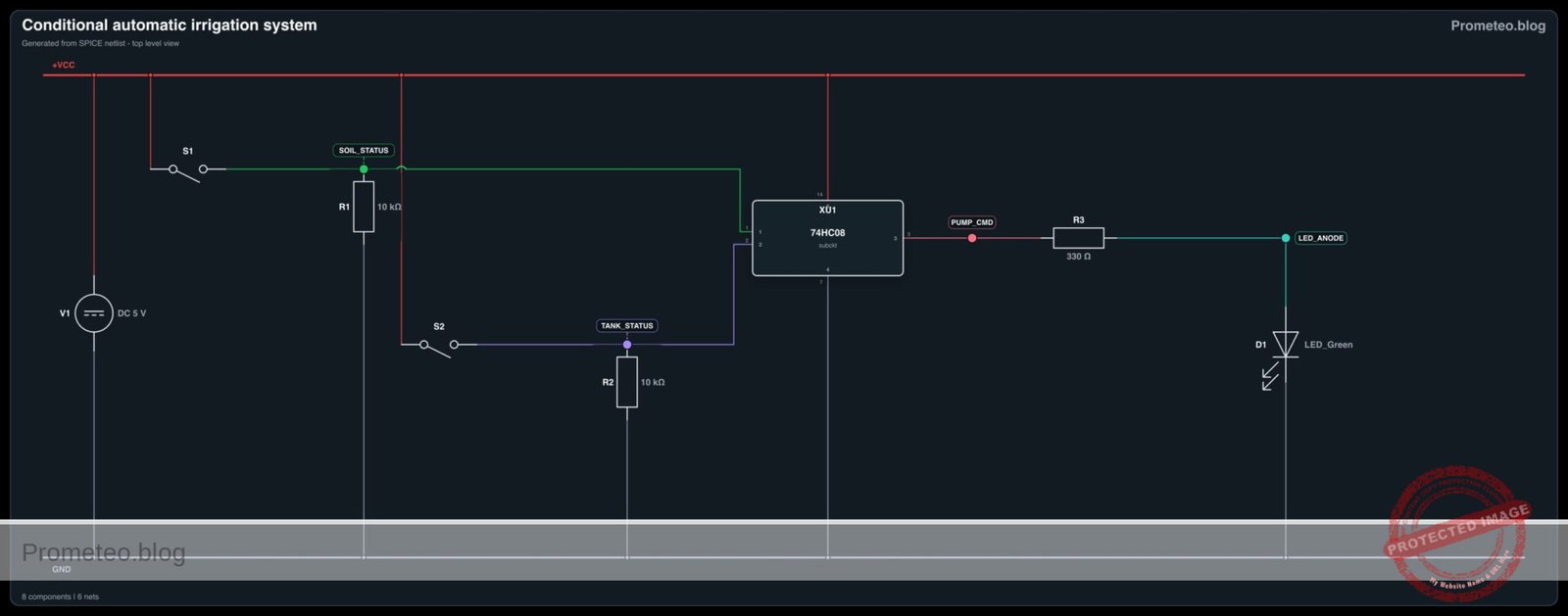
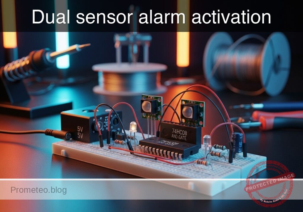
More Practical Cases on Prometeo.blog
Find this product and/or books on this topic on Amazon
As an Amazon Associate, I earn from qualifying purchases. If you buy through this link, you help keep this project running.
Quick Quiz

Telecommunications Electronics Engineer and Computer Engineer (official degrees in Spain).