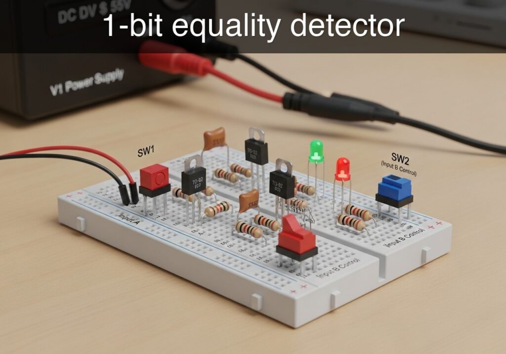
Practical case: 1-bit equality detector

1-bit equality detector prototype (Maker Style)

Level: Basic – Verify the operation of a 74HC7266 XNOR gate as a logical equality detector using its truth table.

Objective and use case

In this practical case, you will build a digital equality detector using a 74HC7266 XNOR logic gate, mechanical switches, and an LED indicator.

This circuit concept is highly useful in real-world digital electronics:
* Digital locks: Comparing an entered bit to a stored security key bit.
* Error detection: Verifying if two redundant sensor signals output the exact same digital state.
* Data routing: Confirming destination addresses in memory mapping or basic communication protocols.
* Automation: Checking if a machine’s actual state matches the commanded state.

Expected outcome:
* The output LED turns ON when both inputs are perfectly equal (both LOW or both HIGH).
* The output LED remains OFF when the inputs differ (one is HIGH and the other is LOW).
* Logic LOW is measured as approximately 0 V, and logic HIGH as approximately 5 V.

Target audience: Beginners learning fundamental digital logic gates and Boolean algebra.

Materials

  • V1: 5 V DC power supply, function: circuit power
  • SW1: SPST switch, function: input A control
  • SW2: SPST switch, function: input B control
  • R1: 10 kΩ resistor, function: pull-down for node VA
  • R2: 10 kΩ resistor, function: pull-down for node VB
  • R3: 330 Ω resistor, function: LED current limiting
  • D1: red LED, function: equality indicator
  • U1: 74HC7266 IC, function: XNOR logic gate

Pin-out of the 74HC7266

The 74HC7266 is a Quad 2-Input EXCLUSIVE-NOR (XNOR) gate with push-pull outputs.

Pin Name Logic function Connection in this case
1 1 A Input A of gate 1 Node VA
2 1B Input B of gate 1 Node VB
3 1Y Output of gate 1 Node VOUT
5, 6 2 A, 2B Inputs of gate 2 Node 0 (GND)
7 GND Ground Node 0 (GND)
8, 9 3 A, 3B Inputs of gate 3 Node 0 (GND)
12, 13 4 A, 4B Inputs of gate 4 Node 0 (GND)
14 VCC Positive supply Node VCC

Note: Unused inputs (pins 5, 6, 8, 9, 12, 13) must be tied to ground to prevent CMOS oscillation and excess power draw.

Wiring guide

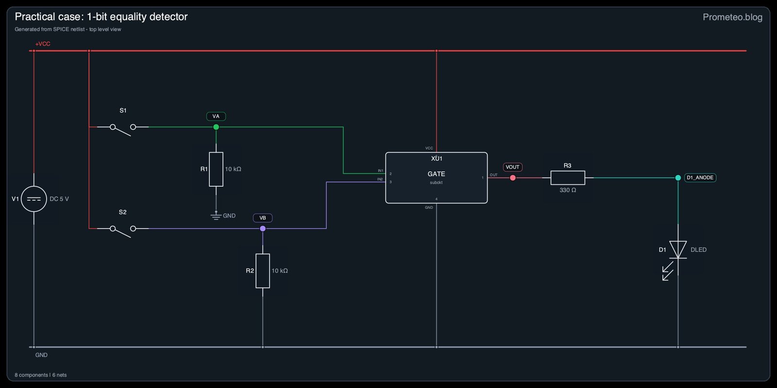
  • V1: connects between node VCC and node 0 (GND).
  • SW1: connects between node VCC and node VA.
  • R1: connects between node VA and node 0.
  • SW2: connects between node VCC and node VB.
  • R2: connects between node VB and node 0.
  • U1: VCC pin (14) connects to node VCC.
  • U1: GND pin (7) connects to node 0.
  • U1: Pin 1 (1 A) connects to node VA.
  • U1: Pin 2 (1B) connects to node VB.
  • U1: Pin 3 (1Y) connects to node VOUT.
  • U1: Pins 5, 6, 8, 9, 12, and 13 connect directly to node 0.
  • R3: connects between node VOUT and node D1_ANODE.
  • D1: anode connects to node D1_ANODE, cathode connects to node 0.

Conceptual block diagram
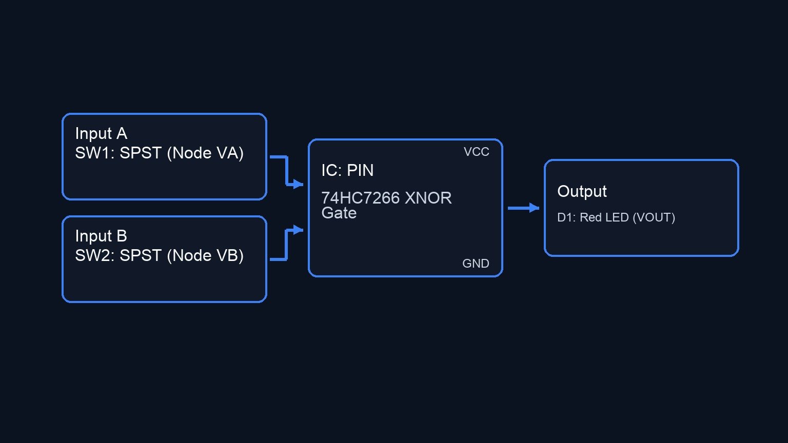
Conceptual block diagram — PIN 74HC7266 XNOR Gate
Quick read: inputs → main block → output (actuator or measurement). This summarizes the ASCII schematic below.

Schematic

VCC --> [ SW1: SPST ] --(Node VA)--> [ U1: Pin 1 (1 A) ]
                                            |
        (Node VA) --> [ R1: 10 kΩ ] --> GND  |
                                     [ U1: 74HC7266 XNOR ] --(Node VOUT)--> [ R3: 330 Ω ] --> [ D1: Red LED ] --> GND
        (Node VB) --> [ R2: 10 kΩ ] --> GND  |
                                            |
VCC --> [ SW2: SPST ] --(Node VB)--> [ U1: Pin 2 (1B) ]

* Power & Unused Pins:
  VCC --> [ U1: Pin 14 (VCC) ]
  GND <-- [ U1: Pin 7 (GND) ]
  GND <-- [ U1: Pins 5, 6, 8, 9, 12, 13 (Unused Inputs) ]
Electrical Schematic

Electrical diagram

Electrical diagram for case: 1-bit equality detector
Generated from the validated SPICE netlist for this case.

Truth table

VA (Input A) VB (Input B) VOUT (Output) D1 (LED Status)
0 0 1 ON
0 1 0 OFF
1 0 0 OFF
1 1 1 ON

Measurements and tests

  1. Initial Power Verification: Before actuating any switches, power on the circuit. Measure the voltage between VCC and 0 to ensure it is 5 V.
  2. Input State Testing: Set your multimeter to DC Voltage. Measure nodes VA and VB with respect to node 0. Toggle SW1 and SW2 to verify that an open switch yields ~0 V (thanks to the pull-down resistors) and a closed switch yields ~5 V.
  3. XNOR Logic Verification: Measure the voltage at VOUT with respect to node 0 for all four combinations of SW1 and SW2.
  4. Equality Confirmation: Ensure VOUT is approximately 5 V and the LED is illuminated ONLY when VA and VB are perfectly matched (0 V & 0 V, or 5 V & 5 V).

SPICE netlist and simulation

Reference SPICE Netlist (ngspice) — excerptFull SPICE netlist (ngspice)

* Practical case: 1-bit equality detector
.width out=256

V1 VCC 0 DC 5

* Control signals for SW1 and SW2 to simulate user interaction
VctrlA ctrlA 0 PULSE(0 5 0 1u 1u 50u 100u)
VctrlB ctrlB 0 PULSE(0 5 0 1u 1u 100u 200u)

* SW1 and SW2 modeled as voltage-controlled switches
S1 VCC VA ctrlA 0 SWMOD
S2 VCC VB ctrlB 0 SWMOD

* Pull-down resistors R1 and R2
R1 VA 0 10k
R2 VB 0 10k

* U1: 74HC7266 XNOR Gate equivalent
XU1 VOUT VA VB 0 VCC GATE

* ... (truncated in public view) ...

Copy this content into a .cir file and run with ngspice.

* Practical case: 1-bit equality detector
.width out=256

V1 VCC 0 DC 5

* Control signals for SW1 and SW2 to simulate user interaction
VctrlA ctrlA 0 PULSE(0 5 0 1u 1u 50u 100u)
VctrlB ctrlB 0 PULSE(0 5 0 1u 1u 100u 200u)

* SW1 and SW2 modeled as voltage-controlled switches
S1 VCC VA ctrlA 0 SWMOD
S2 VCC VB ctrlB 0 SWMOD

* Pull-down resistors R1 and R2
R1 VA 0 10k
R2 VB 0 10k

* U1: 74HC7266 XNOR Gate equivalent
XU1 VOUT VA VB 0 VCC GATE

* LED current limiting resistor R3
R3 VOUT D1_ANODE 330

* Equality indicator LED D1
D1 D1_ANODE 0 DLED

* Subcircuit for canonical 2-input XNOR gate
.subckt GATE out in1 in2 gnd vcc
B1 out gnd V = 5 * (1 / (1 + exp(-5 * (V(in1)-2.5) * (V(in2)-2.5))))
.ends

* Models
.model SWMOD SW(VT=2.5 VH=0.2 RON=0.1 ROFF=100MEG)
.model DLED D(IS=1e-15 N=2.0 RS=10)

* Simulation commands
.op
.tran 1u 500u
.print tran V(VOUT) V(VA) V(VB) V(D1_ANODE)
.end

Simulation Results (Transient Analysis)

Simulation Results (Transient Analysis)
Analysis: The transient analysis spans 0 s to 500 us and captures the switching interval. Main ranges: v(vout) 1.35e-07 uV -> 5 V; v(va) 500 uV -> 5 V; v(vb) 500 uV -> 5 V.
Show raw data table (694 rows)
Index   time            v(vout)         v(va)           v(vb)           v(d1_anode)
0	0.000000e+00	5.000000e+00	4.999500e-04	4.999500e-04	1.650722e+00
1	1.000000e-08	5.000000e+00	4.999500e-04	4.999500e-04	1.650721e+00
2	2.000000e-08	5.000000e+00	4.999500e-04	4.999500e-04	1.650721e+00
3	4.000000e-08	5.000000e+00	4.999500e-04	4.999500e-04	1.650721e+00
4	8.000000e-08	5.000000e+00	4.999500e-04	4.999500e-04	1.650721e+00
5	1.600000e-07	5.000000e+00	4.999500e-04	4.999500e-04	1.650721e+00
6	3.200000e-07	5.000000e+00	4.999500e-04	4.999500e-04	1.650721e+00
7	3.637500e-07	5.000000e+00	4.999500e-04	4.999500e-04	1.650721e+00
8	4.403125e-07	5.000000e+00	4.999500e-04	4.999500e-04	1.650721e+00
9	4.615039e-07	5.000000e+00	4.999500e-04	4.999500e-04	1.650721e+00
10	4.985889e-07	5.000000e+00	4.999500e-04	4.999500e-04	1.650721e+00
11	5.088535e-07	5.000000e+00	4.999500e-04	4.999500e-04	1.650721e+00
12	5.268165e-07	5.000000e+00	4.999500e-04	4.999500e-04	1.650721e+00
13	5.467041e-07	5.000000e+00	4.999950e+00	4.999950e+00	1.650721e+00
14	5.864794e-07	5.000000e+00	4.999950e+00	4.999950e+00	1.650721e+00
15	6.660299e-07	5.000000e+00	4.999950e+00	4.999950e+00	1.650721e+00
16	8.251311e-07	5.000000e+00	4.999950e+00	4.999950e+00	1.650721e+00
17	1.000000e-06	5.000000e+00	4.999950e+00	4.999950e+00	1.650721e+00
18	1.031820e-06	5.000000e+00	4.999950e+00	4.999950e+00	1.650721e+00
19	1.095461e-06	5.000000e+00	4.999950e+00	4.999950e+00	1.650721e+00
20	1.222742e-06	5.000000e+00	4.999950e+00	4.999950e+00	1.650721e+00
21	1.477303e-06	5.000000e+00	4.999950e+00	4.999950e+00	1.650721e+00
22	1.986427e-06	5.000000e+00	4.999950e+00	4.999950e+00	1.650721e+00
23	2.986427e-06	5.000000e+00	4.999950e+00	4.999950e+00	1.650721e+00
... (670 more rows) ...


Reference SPICE netlist (ngspice)

* Practical case: 1-bit equality detector
.width out=256

V1 VCC 0 DC 5

* Control signals for SW1 and SW2 to simulate user interaction
VctrlA ctrlA 0 PULSE(0 5 0 1u 1u 50u 100u)
VctrlB ctrlB 0 PULSE(0 5 0 1u 1u 100u 200u)

* SW1 and SW2 modeled as voltage-controlled switches
S1 VCC VA ctrlA 0 SWMOD
S2 VCC VB ctrlB 0 SWMOD

* Pull-down resistors R1 and R2
R1 VA 0 10k
R2 VB 0 10k

* U1: 74HC7266 XNOR Gate equivalent
XU1 VOUT VA VB 0 VCC GATE

* LED current limiting resistor R3
R3 VOUT D1_ANODE 330

* Equality indicator LED D1
D1 D1_ANODE 0 DLED

* Subcircuit for canonical 2-input XNOR gate
.subckt GATE out in1 in2 gnd vcc
B1 out gnd V = 5 * (1 / (1 + exp(-5 * (V(in1)-2.5) * (V(in2)-2.5))))
.ends

* Models
.model SWMOD SW(VT=2.5 VH=0.2 RON=0.1 ROFF=100MEG)
.model DLED D(IS=1e-15 N=2.0 RS=10)

* Simulation commands
.op
.tran 1u 500u
.print tran V(VOUT) V(VA) V(VB) V(D1_ANODE)
.end

Simulation Results (Transient Analysis)

Simulation Results (Transient Analysis)
Analysis: The transient analysis spans 0 s to 500 us and captures the switching interval. Main ranges: v(vout) 1.35e-07 uV -> 5 V; v(va) 500 uV -> 5 V; v(vb) 500 uV -> 5 V.

Common mistakes and how to avoid them

  • Confusing 74HC7266 with 74HC266: The 74HC266 has open-drain outputs, which means it cannot source current to turn on an LED without an external pull-up resistor. Ensure you use the 74HC7266 (push-pull) or add a pull-up resistor if using the 74HC266.
  • Leaving CMOS inputs floating: Forgetting to ground the unused inputs of the 74HC7266 can cause internal high-frequency oscillation, drawing excessive current and potentially damaging the IC. Always tie unused inputs to GND or VCC.
  • Omitting pull-down resistors: If R1 and R2 are forgotten, the inputs will float unpredictably when the switches are open, causing the LED to flicker randomly.


Troubleshooting

  • Symptom: LED flickers or behaves erratically when switches are open.
    • Cause: Node VA or VB is floating.
    • Fix: Verify that R1 and R2 are securely connected between the switch inputs and ground.
  • Symptom: LED never turns on.
    • Cause: LED D1 is inserted backwards (reversed polarity) or R3 is too large (e.g., 100 kΩ instead of 330 Ω).
    • Fix: Check the orientation of D1 (longer leg to D1_ANODE) and verify the value of R3.
  • Symptom: LED is always ON regardless of switch positions.
    • Cause: Output pin (3) is shorted to VCC, or both switches are permanently shorted to the same logic level.
    • Fix: Inspect the wiring around VOUT, VA, and VB. Ensure the switches physically break the connection to VCC when toggled off.

Possible improvements and extensions

  • Audible Equality Alert: Connect a 5 V active piezoelectric buzzer in parallel with the LED/resistor combination to provide an audible tone whenever the input bits match.
  • 2-Bit Equality Detector: Use a second XNOR gate from the same IC for a second pair of inputs, and feed the outputs of both XNOR gates into an AND gate to verify if two 2-bit words are exactly equal.

More Practical Cases on Prometeo.blog

Find this product and/or books on this topic on Amazon

Go to Amazon

As an Amazon Associate, I earn from qualifying purchases. If you buy through this link, you help keep this project running.

Quick Quiz

Question 1: What is the primary function of the 74HC7266 IC in this circuit?


Question 2: What is the expected behavior of the LED when both inputs to the XNOR gate are LOW?


Question 3: What happens to the output LED when one input is HIGH and the other is LOW?


Question 4: In this circuit, what voltage approximately represents a logic HIGH?


Question 5: In this circuit, what voltage approximately represents a logic LOW?


Question 6: Which real-world application uses this circuit concept to compare an entered bit to a stored security key bit?


Question 7: How is the XNOR gate concept used in error detection according to the text?


Question 8: What is the main objective of this practical case?


Question 9: Who is the target audience for this practical case?


Question 10: In automation, how is the XNOR gate concept applied based on the text?


Carlos Núñez Zorrilla
Electronics & Computer Engineer

Telecommunications Electronics Engineer and Computer Engineer (official degrees in Spain).
Follow me:


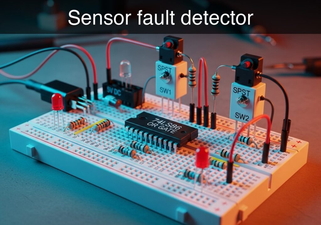
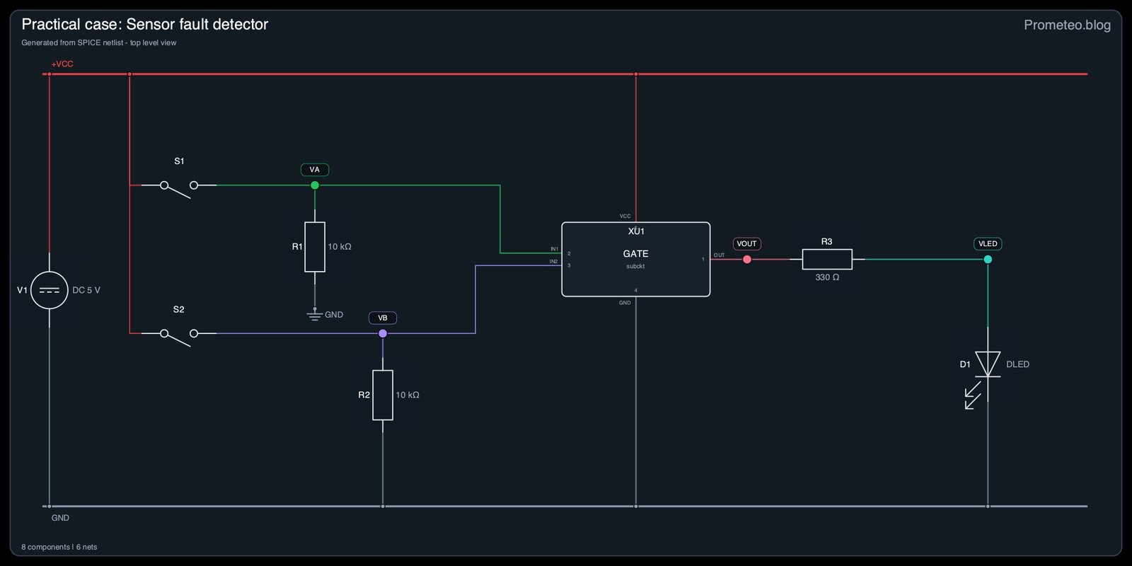
Practical case: Sensor fault detector

Sensor fault detector prototype (Maker Style)

Level: Basic – Implement an XOR gate circuit to activate a visual alarm when two redundant sensors present different logic states.

Objective and use case

You will build a digital logic comparator circuit using a 74LS86 XOR (Exclusive-OR) gate to monitor two redundant switches acting as system sensors. The circuit evaluates the inputs continuously and activates a visual LED alarm only when the two sensors report conflicting states, indicating a potential sensor failure.

This circuit is highly useful in practical scenarios such as:
* Industrial automation, for monitoring dual-redundant safety limit switches on heavy machinery.
* Aerospace and aviation control systems, to detect disagreements between redundant flight sensors.
* Basic logic fault-detection training for maintenance and electronics technicians.

Expected outcome:
* A high output logic level (VOUT > 2.4 V) triggering the LED when the sensor states do not match.
* A low output logic level (VOUT < 0.4 V) keeping the LED turned off when both sensors agree (both HIGH or both LOW).
* A clear, immediate visual indication of logic discrepancies to the operator.

Target audience: Basic-level students learning digital logic gates, boolean algebra, and redundancy systems.

Materials

  • V1: 5 V DC supply, function: primary power source
  • SW1: SPST switch, function: redundant sensor A simulator
  • SW2: SPST switch, function: redundant sensor B simulator
  • R1: 10 kΩ resistor, function: pull-down for VA
  • R2: 10 kΩ resistor, function: pull-down for VB
  • R3: 330 Ω resistor, function: LED current limiting
  • U1: 74LS86 Quad 2-Input Exclusive-OR Gate, function: fault detection logic
  • D1: red LED, function: visual fault alarm indicator

Pin-out of the IC used

Integrated Circuit: 74LS86

Pin Name Logic function Connection in this case
1 1 A Input 1 for Gate 1 Node VA (from SW1)
2 1B Input 2 for Gate 1 Node VB (from SW2)
3 1Y Output of Gate 1 Node VOUT (to R3 and D1)
7 GND Ground Node 0 (GND)
14 VCC Power Supply Node VCC (5 V)

Note: Pins 4, 5, 6, 8, 9, 10, 11, 12, and 13 belong to the other three unused XOR gates. It is highly recommended to tie unused inputs (pins 4, 5, 9, 10, 12, 13) to Node 0 (GND).

Wiring guide

  • V1: connects between VCC and 0.
  • SW1: connects between VCC and VA.
  • SW2: connects between VCC and VB.
  • R1: connects between VA and 0.
  • R2: connects between VB and 0.
  • U1: connects Pin 14 to VCC, Pin 7 to 0, Pin 1 to VA, Pin 2 to VB, and Pin 3 to VOUT.
  • R3: connects between VOUT and VLED.
  • D1: connects its anode to VLED and its cathode to 0.

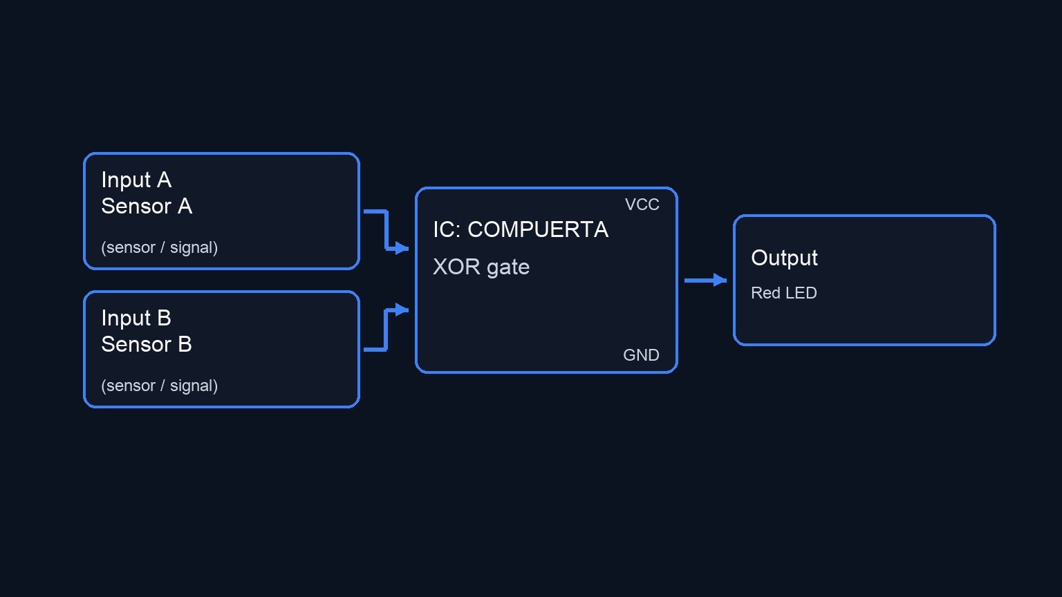
Conceptual block diagram

Conceptual block diagram — COMPUERTA XOR gate
Quick read: inputs → main block → output (actuator or measurement). This summarizes the ASCII schematic below.

Schematic

VCC --> [ SW1: Sensor A ] --(VA)-->
              |                   |
              v                   v
        [ R1: 10 kΩ ]            [ U1: 74LS86 XOR Gate ] --(VOUT)--> [ R3: 330 Ω ] --(VLED)--> [ D1: Red LED ] --> GND
              |                   ^
              v                   |
             GND                  |
                                  |
VCC --> [ SW2: Sensor B ] --(VB)-->
              |
              v
        [ R2: 10 kΩ ]
              |
              v
             GND
Electrical Schematic

Electrical diagram

Electrical diagram for case: Sensor fault detector
Generated from the validated SPICE netlist for this case.

Truth table

Sensor A (Node VA) Sensor B (Node VB) Output (Node VOUT) Alarm State (D1) System Status
0 0 0 OFF Normal (Agreement)
0 1 1 ON Fault (Disagreement)
1 0 1 ON Fault (Disagreement)
1 1 0 OFF Normal (Agreement)

Measurements and tests

  1. System Normal (Low): Leave both SW1 and SW2 open. Measure the voltage at nodes VA and VB with a multimeter; both should read 0 V. Measure VOUT; it should be < 0.4 V. The LED D1 must be OFF.
  2. Sensor A Fault: Close SW1 (applying 5 V to VA) while leaving SW2 open (0 V at VB). Measure VOUT; it should read > 2.4 V. The LED D1 must turn ON.
  3. Sensor B Fault: Open SW1 (0 V at VA) and close SW2 (applying 5 V to VB). Measure VOUT; it should read > 2.4 V. The LED D1 must turn ON.
  4. System Normal (High): Close both SW1 and SW2 so that both VA and VB read 5 V. Measure VOUT; it should drop back to < 0.4 V. The LED D1 must be OFF.

SPICE netlist and simulation

Reference SPICE Netlist (ngspice) — excerptFull SPICE netlist (ngspice)

* Practical case: Sensor fault detector
.width out=256

* Main Power Supply
V1 VCC 0 DC 5

* Redundant Sensor A Simulator (Switch 1)
VCTRLA ctrlA 0 PULSE(0 5 0 1u 1u 50u 100u)
S1 VCC VA ctrlA 0 SWMOD

* Redundant Sensor B Simulator (Switch 2)
VCTRLB ctrlB 0 PULSE(0 5 0 1u 1u 100u 200u)
S2 VCC VB ctrlB 0 SWMOD

* Pull-down Resistors for Inputs
R1 VA 0 10k
R2 VB 0 10k

* Fault Detection Logic (74LS86 XOR Gate)
XU1 VOUT VA VB 0 VCC GATE
* ... (truncated in public view) ...

Copy this content into a .cir file and run with ngspice.

* Practical case: Sensor fault detector
.width out=256

* Main Power Supply
V1 VCC 0 DC 5

* Redundant Sensor A Simulator (Switch 1)
VCTRLA ctrlA 0 PULSE(0 5 0 1u 1u 50u 100u)
S1 VCC VA ctrlA 0 SWMOD

* Redundant Sensor B Simulator (Switch 2)
VCTRLB ctrlB 0 PULSE(0 5 0 1u 1u 100u 200u)
S2 VCC VB ctrlB 0 SWMOD

* Pull-down Resistors for Inputs
R1 VA 0 10k
R2 VB 0 10k

* Fault Detection Logic (74LS86 XOR Gate)
XU1 VOUT VA VB 0 VCC GATE

* Visual Fault Alarm Indicator (LED and Current Limiting Resistor)
R3 VOUT VLED 330
D1 VLED 0 DLED

* Component Models
.model SWMOD SW(VT=2.5 VH=0.2 RON=0.1 ROFF=100MEG)
.model DLED D(IS=1e-15 N=1.5 RS=10)

* XOR Gate Behavioural Subcircuit
* Continuous implementation to ensure robust convergence
.subckt GATE out in1 in2 gnd vcc
B1 out gnd V = V(vcc) * ( 1/(1+exp(-50*(V(in1)-2.5))) + 1/(1+exp(-50*(V(in2)-2.5))) - 2 * (1/(1+exp(-50*(V(in1)-2.5)))) * (1/(1+exp(-50*(V(in2)-2.5)))) )
.ends

* Simulation Directives
.tran 1u 400u
.print tran V(VA) V(VB) V(VOUT) V(VLED)
.op
.end

Simulation Results (Transient Analysis)

Simulation Results (Transient Analysis)
Analysis: The transient simulation shows the XOR logic functioning correctly. When VA and VB are both low (~0V) or both high (~5V), VOUT is ~0V and VLED is ~0V (LED off). When VA and VB differ (one is ~5V, the other ~0V), VOUT goes to 5V and VLED reaches ~1.28V, indicating the LED is forward-biased and turned on, matching the truth table.
Show raw data table (562 rows)
Index   time            v(va)           v(vb)           v(vout)         v(vled)
0	0.000000e+00	4.999500e-04	4.999500e-04	5.297196e-54	9.094010e-30
1	1.000000e-08	4.999500e-04	4.999500e-04	5.297196e-54	7.969517e-41
2	2.000000e-08	4.999500e-04	4.999500e-04	5.297196e-54	-7.96952e-41
3	4.000000e-08	4.999500e-04	4.999500e-04	5.297196e-54	-3.48674e-51
4	8.000000e-08	4.999500e-04	4.999500e-04	5.297196e-54	1.402111e-51
5	1.600000e-07	4.999500e-04	4.999500e-04	5.297196e-54	5.297196e-54
6	3.200000e-07	4.999500e-04	4.999500e-04	5.297196e-54	5.297196e-54
7	3.637500e-07	4.999500e-04	4.999500e-04	5.297196e-54	5.297196e-54
8	4.403125e-07	4.999500e-04	4.999500e-04	5.297196e-54	5.297196e-54
9	4.615039e-07	4.999500e-04	4.999500e-04	5.297196e-54	5.297196e-54
10	4.985889e-07	4.999500e-04	4.999500e-04	5.297196e-54	5.297196e-54
11	5.088535e-07	4.999500e-04	4.999500e-04	5.297196e-54	5.297196e-54
12	5.268165e-07	4.999500e-04	4.999500e-04	5.297196e-54	5.297196e-54
13	5.467041e-07	4.999950e+00	4.999950e+00	1.329451e-51	1.329451e-51
14	5.864794e-07	4.999950e+00	4.999950e+00	-2.81145e-68	3.383370e-62
15	6.660299e-07	4.999950e+00	4.999950e+00	-2.81145e-68	-2.26159e-62
16	8.251311e-07	4.999950e+00	4.999950e+00	-2.81145e-68	-2.81157e-68
17	1.000000e-06	4.999950e+00	4.999950e+00	-2.81145e-68	-2.81143e-68
18	1.031820e-06	4.999950e+00	4.999950e+00	-2.81145e-68	-2.81145e-68
19	1.095461e-06	4.999950e+00	4.999950e+00	-2.81145e-68	-2.81145e-68
20	1.222742e-06	4.999950e+00	4.999950e+00	-2.81145e-68	-2.81145e-68
21	1.477303e-06	4.999950e+00	4.999950e+00	-2.81145e-68	-2.81145e-68
22	1.986427e-06	4.999950e+00	4.999950e+00	-2.81145e-68	-2.81145e-68
23	2.986427e-06	4.999950e+00	4.999950e+00	-2.81145e-68	-2.81145e-68
... (538 more rows) ...


Reference SPICE netlist (ngspice)

* Practical case: Sensor fault detector
.width out=256

* Main Power Supply
V1 VCC 0 DC 5

* Redundant Sensor A Simulator (Switch 1)
VCTRLA ctrlA 0 PULSE(0 5 0 1u 1u 50u 100u)
S1 VCC VA ctrlA 0 SWMOD

* Redundant Sensor B Simulator (Switch 2)
VCTRLB ctrlB 0 PULSE(0 5 0 1u 1u 100u 200u)
S2 VCC VB ctrlB 0 SWMOD

* Pull-down Resistors for Inputs
R1 VA 0 10k
R2 VB 0 10k

* Fault Detection Logic (74LS86 XOR Gate)
XU1 VOUT VA VB 0 VCC GATE

* Visual Fault Alarm Indicator (LED and Current Limiting Resistor)
R3 VOUT VLED 330
D1 VLED 0 DLED

* Component Models
.model SWMOD SW(VT=2.5 VH=0.2 RON=0.1 ROFF=100MEG)
.model DLED D(IS=1e-15 N=1.5 RS=10)

* XOR Gate Behavioural Subcircuit
* Continuous implementation to ensure robust convergence
.subckt GATE out in1 in2 gnd vcc
B1 out gnd V = V(vcc) * ( 1/(1+exp(-50*(V(in1)-2.5))) + 1/(1+exp(-50*(V(in2)-2.5))) - 2 * (1/(1+exp(-50*(V(in1)-2.5)))) * (1/(1+exp(-50*(V(in2)-2.5)))) )
.ends

* Simulation Directives
.tran 1u 400u
.print tran V(VA) V(VB) V(VOUT) V(VLED)
.op
.end

Simulation Results (Transient Analysis)

Simulation Results (Transient Analysis)
Analysis: The transient simulation shows the XOR logic functioning correctly. When VA and VB are both low (~0V) or both high (~5V), VOUT is ~0V and VLED is ~0V (LED off). When VA and VB differ (one is ~5V, the other ~0V), VOUT goes to 5V and VLED reaches ~1.28V, indicating the LED is forward-biased and turned on, matching the truth table.

Common mistakes and how to avoid them

  • Forgetting pull-down resistors: Connecting the switches directly to the IC without R1 and R2 leaves the inputs floating when the switches are open, causing unpredictable behavior and false alarms. Always use pull-down resistors.
  • LED polarity reversal: Putting the LED in backward (cathode to VLED, anode to 0) will prevent it from lighting up even when a fault is detected. Verify the flat edge or shorter leg is connected to ground.
  • Leaving unused inputs floating: The 74LS86 contains four XOR gates. Leaving the inputs of the unused gates disconnected can cause internal oscillation and increase power consumption. Tie unused inputs to ground (0).


Troubleshooting

  • Symptom: The LED never turns on under any switch combination.
    • Cause: Faulty LED, backward LED polarity, broken R3 connection, or missing VCC/GND to the chip.
    • Fix: Check D1 orientation. Verify 5 V at Pin 14 and 0 V at Pin 7 of U1.
  • Symptom: The LED is always on, even when both switches are open or both are closed.
    • Cause: One of the inputs is floating (missing pull-down resistor R1 or R2), or a switch is wired incorrectly.
    • Fix: Check continuity on R1 and R2 to ground. Verify the voltages at VA and VB correspond strictly to the truth table.
  • Symptom: The LED lights up correctly but is very dim.
    • Cause: The 74LS series has weak current sourcing capabilities compared to modern CMOS chips, or the value of R3 is too high.
    • Fix: Reduce R3 slightly (e.g., to 220 Ω), or see the extensions below for a better way to drive the LED.

Possible improvements and extensions

  • Active-low output configuration: Since TTL chips (like the 74LS series) are much better at sinking current than sourcing it, rewire the LED so the anode goes to 5 V (through R3) and the cathode goes to VOUT. Note: you will need to add a NOT gate (e.g., 74LS04) after the XOR to invert the logic so the LED still turns on only during a fault.
  • Audible alarm integration: Add an NPN transistor (like a 2N2222) connected to the XOR output via a base resistor. Use the transistor to drive a 5 V buzzer to provide both audible and visual alerts when the sensors disagree.

More Practical Cases on Prometeo.blog

Find this product and/or books on this topic on Amazon

Go to Amazon

As an Amazon Associate, I earn from qualifying purchases. If you buy through this link, you help keep this project running.

Quick Quiz

Question 1: What is the primary purpose of the XOR gate circuit described in the text?


Question 2: Which specific logic gate IC is used in this circuit?


Question 3: What does it indicate when the LED alarm is activated?


Question 4: In which of the following practical scenarios is this circuit highly useful?


Question 5: What is the expected high output logic level (VOUT) required to trigger the LED?


Question 6: According to the circuit diagram, what is the resistance value of the pull-down resistors R1 and R2?


Question 7: What is the purpose of resistor R3 (330 Ω) in the circuit?


Question 8: Based on the truth table, what happens when Sensor A is 1 and Sensor B is 1?


Carlos Núñez Zorrilla
Electronics & Computer Engineer

Telecommunications Electronics Engineer and Computer Engineer (official degrees in Spain).
Follow me:


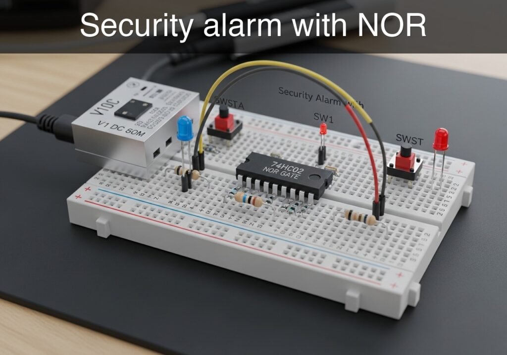
Practical case: Security alarm with NOR

Security alarm with NOR prototype (Maker Style)

Level: Basic | Objective: Verify the NOR gate truth table using an alarm circuit that activates only when no sensors detect movement.

Objective and use case

We will build a simple security alarm simulator using a 74HC02 NOR gate. In this system, the alarm (an LED) will illuminate only when all connected monitoring sensors (represented by switches) indicate a safe, undisturbed state (Logic 0).

Why it is useful:
* Demonstrates negative logic applications where the absence of inputs is required to trigger an action.
* Provides practical experience with CMOS logic gate behavior and logic-level thresholds.
* Mimics real-world safety interlocks, such as machine guards, where multiple conditions must be false for the system to operate.
* Introduces the essential use of pull-down resistors to ensure stable, predictable logic states.

Expected outcome:
* The output LED will illuminate only when both sensor switches are open (Logic 0, 0 V).
* The output LED will turn off immediately if either or both switches are closed (Logic 1, 5 V).
* Input voltages will measure close to 0 V when switches are open, and near 5 V when closed.
* The output voltage will strictly follow the theoretical truth table of a NOR logic gate.

Target audience: Beginners in digital electronics learning fundamental logic gates and basic control circuits.

Materials

  • V1: 5 V DC power supply
  • U1: 74HC02 Quad 2-Input NOR Gate
  • SW1: SPST switch, function: sensor A input
  • SW2: SPST switch, function: sensor B input
  • R1: 10 kΩ resistor, function: pull-down for VA
  • R2: 10 kΩ resistor, function: pull-down for VB
  • R3: 330 Ω resistor, function: LED current limiting
  • D1: Red LED, function: alarm active indicator

Pin-out of the IC used

IC Selected: 74HC02

Pin Name Logic function Connection in this case
1 1Y Output of Gate 1 Connects to VOUT
2 1 A Input A of Gate 1 Connects to VA
3 1B Input B of Gate 1 Connects to VB
7 GND Ground reference Connects to 0
14 VCC Positive supply voltage Connects to VCC

(Note: Pins 4, 5, 6, 8, 9, 10, 11, 12, and 13 belong to the unused gates in the IC package and should ideally have their inputs tied to ground in a permanent design to prevent CMOS floating states).

Wiring guide

  • V1: Connects between VCC and 0.
  • U1 (Pin 14): Connects to VCC.
  • U1 (Pin 7): Connects to 0.
  • SW1: Connects between VCC and VA.
  • SW2: Connects between VCC and VB.
  • R1: Connects between VA and 0.
  • R2: Connects between VB and 0.
  • U1 (Pin 2): Connects to VA.
  • U1 (Pin 3): Connects to VB.
  • U1 (Pin 1): Connects to VOUT.
  • R3: Connects between VOUT and D1_A.
  • D1: Connects between D1_A (anode) and 0 (cathode).

Conceptual block diagram

Conceptual block diagram — COMPUERTA 74HC02 NOR Logic
Quick read: inputs → main block → output (actuator or measurement). This summarizes the ASCII schematic below.

Schematic

VCC   GND
                                           |     |
                                        (Pin14)(Pin7)
VCC --> [ SW1: Sensor A ] --(VA)--> [                   ]
[ VA ] ---> [ R1: 10 kΩ ] ---> GND   [ Pin 2             ]
                                    [ U1: 74HC02 NOR    ] --(Pin 1: VOUT)--> [ R3: 330 Ω ] --> [ D1: Red LED ] --> GND
VCC --> [ SW2: Sensor B ] --(VB)--> [ Pin 3             ]
[ VB ] ---> [ R2: 10 kΩ ] ---> GND   [                   ]
Electrical Schematic

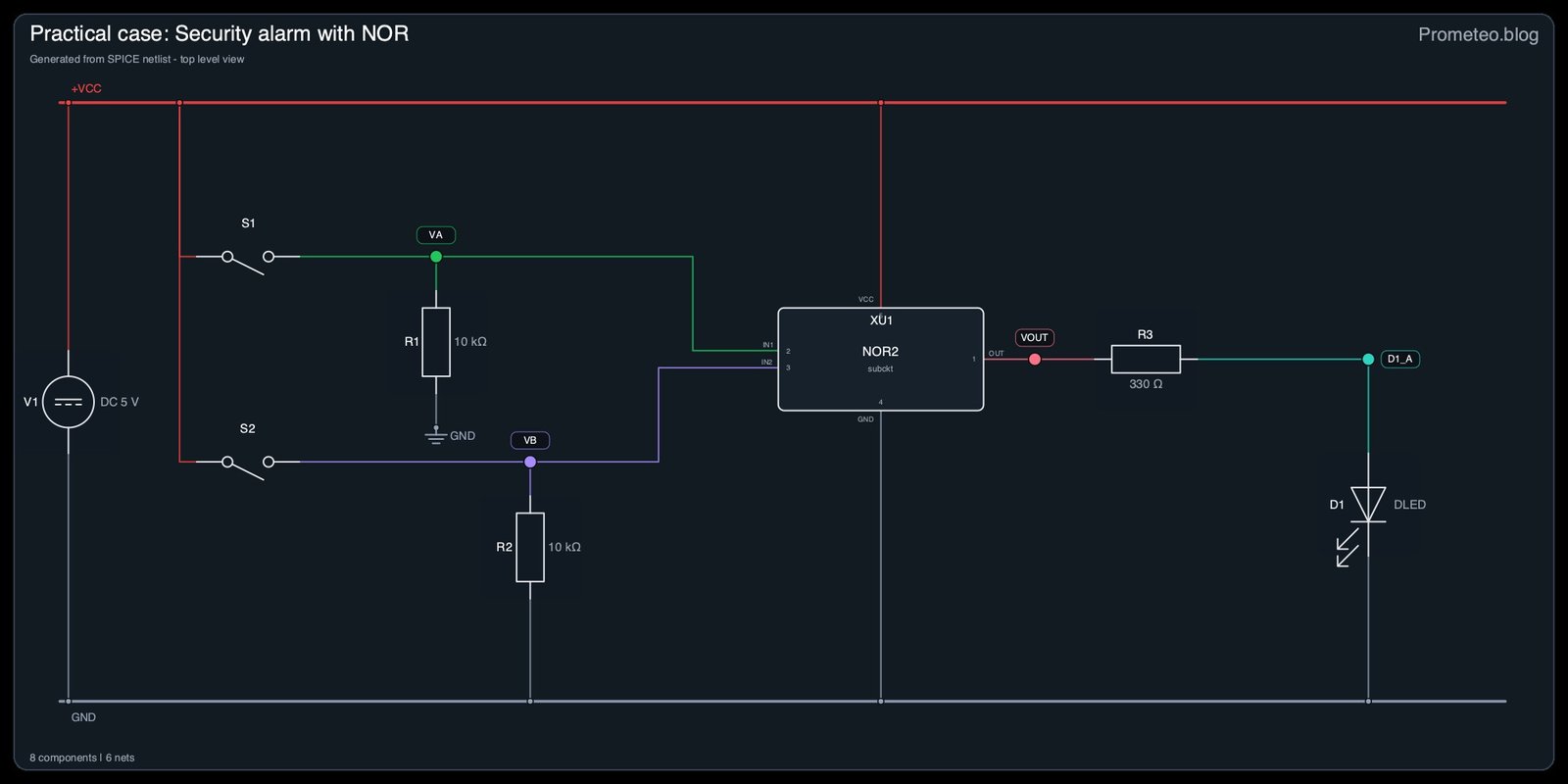
Electrical diagram

Electrical diagram for case: Security alarm with NOR
Generated from the validated SPICE netlist for this case.

Truth table

Input A (VA) Input B (VB) Output Y (VOUT) Alarm State
0 0 1 LED ON
0 1 0 LED OFF
1 0 0 LED OFF
1 1 0 LED OFF

Measurements and tests

  1. Power verification: With the power supply connected, use a multimeter to measure the voltage between nodes VCC and 0. Ensure it is strictly 5 V.
  2. Idle state test (0, 0): Leave both SW1 and SW2 open. Measure nodes VA and VB with respect to ground; they should be 0 V. Measure VOUT; it should read near 5 V, and the LED should be ON.
  3. Single sensor test (1, 0 / 0, 1): Close SW1 (leaving SW2 open). Measure VA; it should be 5 V. Measure VOUT; it should immediately drop to 0 V, and the LED should turn OFF. Repeat by opening SW1 and closing SW2.
  4. Dual sensor test (1, 1): Close both SW1 and SW2. Confirm both VA and VB measure 5 V. Measure VOUT to verify it remains 0 V (LED OFF).

SPICE netlist and simulation

Reference SPICE Netlist (ngspice) — excerptFull SPICE netlist (ngspice)

* Practical case: Security alarm with NOR
.width out=256

* Power supply
V1 VCC 0 DC 5

* Dynamic stimuli for user pressing the switches
VctrlA ctrlA 0 PULSE(0 5 0 1u 1u 50u 100u)
VctrlB ctrlB 0 PULSE(0 5 0 1u 1u 100u 200u)

* Switches representing SW1 and SW2
SW1 VCC VA ctrlA 0 SWMOD
SW2 VCC VB ctrlB 0 SWMOD
.model SWMOD SW(VT=2.5 VH=0.2 RON=1 ROFF=100MEG)

* Pull-down resistors
R1 VA 0 10k
R2 VB 0 10k

* NOR Gate 74HC02 (U1)
* ... (truncated in public view) ...

Copy this content into a .cir file and run with ngspice.

* Practical case: Security alarm with NOR
.width out=256

* Power supply
V1 VCC 0 DC 5

* Dynamic stimuli for user pressing the switches
VctrlA ctrlA 0 PULSE(0 5 0 1u 1u 50u 100u)
VctrlB ctrlB 0 PULSE(0 5 0 1u 1u 100u 200u)

* Switches representing SW1 and SW2
SW1 VCC VA ctrlA 0 SWMOD
SW2 VCC VB ctrlB 0 SWMOD
.model SWMOD SW(VT=2.5 VH=0.2 RON=1 ROFF=100MEG)

* Pull-down resistors
R1 VA 0 10k
R2 VB 0 10k

* NOR Gate 74HC02 (U1)
* Pins: 1=VOUT, 2=VA, 3=VB, 7=0, 14=VCC
XU1 VOUT VA VB 0 VCC NOR2

* Output components
R3 VOUT D1_A 330
D1 D1_A 0 DLED

* Models
.model DLED D(IS=1e-19 N=1.6 RS=10)

* Subcircuits
.subckt NOR2 out in1 in2 gnd vcc
* Robust continuous behavior for NOR logic
B1 out gnd V = V(vcc) * (1 / (1 + exp(20*(V(in1)-2.5)))) * (1 / (1 + exp(20*(V(in2)-2.5))))
.ends

* Analysis
.tran 1u 300u
.print tran V(VA) V(VB) V(VOUT) V(D1_A)
.op
.end

Simulation Results (Transient Analysis)

Simulation Results (Transient Analysis)
Analysis: The transient analysis spans 0 s to 300 us and captures the switching interval. Main ranges: v(vout) 1.9e-37 uV -> 5 V; v(va) 500 uV -> 5 V; v(vb) 500 uV -> 5 V.
Show raw data table (417 rows)
Index   time            v(va)           v(vb)           v(vout)         v(d1_a)
0	0.000000e+00	4.999500e-04	4.999500e-04	5.000000e+00	1.719109e+00
1	1.000000e-08	4.999500e-04	4.999500e-04	5.000000e+00	1.719109e+00
2	2.000000e-08	4.999500e-04	4.999500e-04	5.000000e+00	1.719109e+00
3	4.000000e-08	4.999500e-04	4.999500e-04	5.000000e+00	1.719109e+00
4	8.000000e-08	4.999500e-04	4.999500e-04	5.000000e+00	1.719109e+00
5	1.600000e-07	4.999500e-04	4.999500e-04	5.000000e+00	1.719109e+00
6	3.200000e-07	4.999500e-04	4.999500e-04	5.000000e+00	1.719109e+00
7	3.637500e-07	4.999500e-04	4.999500e-04	5.000000e+00	1.719109e+00
8	4.403125e-07	4.999500e-04	4.999500e-04	5.000000e+00	1.719109e+00
9	4.615039e-07	4.999500e-04	4.999500e-04	5.000000e+00	1.719109e+00
10	4.985889e-07	4.999500e-04	4.999500e-04	5.000000e+00	1.719109e+00
11	5.088535e-07	4.999500e-04	4.999500e-04	5.000000e+00	1.719109e+00
12	5.268165e-07	4.999500e-04	4.999500e-04	5.000000e+00	1.719109e+00
13	5.467041e-07	4.999500e+00	4.999500e+00	1.897609e-43	8.840581e-30
14	5.864794e-07	4.999500e+00	4.999500e+00	1.897609e-43	3.298742e-17
15	6.660299e-07	4.999500e+00	4.999500e+00	1.897609e-43	7.028545e-34
16	8.251311e-07	4.999500e+00	4.999500e+00	1.897609e-43	7.526757e-34
17	1.000000e-06	4.999500e+00	4.999500e+00	1.897609e-43	1.897616e-43
18	1.031820e-06	4.999500e+00	4.999500e+00	1.897609e-43	1.897608e-43
19	1.095461e-06	4.999500e+00	4.999500e+00	1.897609e-43	1.897609e-43
20	1.222742e-06	4.999500e+00	4.999500e+00	1.897609e-43	1.897609e-43
21	1.477303e-06	4.999500e+00	4.999500e+00	1.897609e-43	1.897609e-43
22	1.986427e-06	4.999500e+00	4.999500e+00	1.897609e-43	1.897609e-43
23	2.986427e-06	4.999500e+00	4.999500e+00	1.897609e-43	1.897609e-43
... (393 more rows) ...


Reference SPICE netlist (ngspice)

* Practical case: Security alarm with NOR
.width out=256

* Power supply
V1 VCC 0 DC 5

* Dynamic stimuli for user pressing the switches
VctrlA ctrlA 0 PULSE(0 5 0 1u 1u 50u 100u)
VctrlB ctrlB 0 PULSE(0 5 0 1u 1u 100u 200u)

* Switches representing SW1 and SW2
SW1 VCC VA ctrlA 0 SWMOD
SW2 VCC VB ctrlB 0 SWMOD
.model SWMOD SW(VT=2.5 VH=0.2 RON=1 ROFF=100MEG)

* Pull-down resistors
R1 VA 0 10k
R2 VB 0 10k

* NOR Gate 74HC02 (U1)
* Pins: 1=VOUT, 2=VA, 3=VB, 7=0, 14=VCC
XU1 VOUT VA VB 0 VCC NOR2

* Output components
R3 VOUT D1_A 330
D1 D1_A 0 DLED

* Models
.model DLED D(IS=1e-19 N=1.6 RS=10)

* Subcircuits
.subckt NOR2 out in1 in2 gnd vcc
* Robust continuous behavior for NOR logic
B1 out gnd V = V(vcc) * (1 / (1 + exp(20*(V(in1)-2.5)))) * (1 / (1 + exp(20*(V(in2)-2.5))))
.ends

* Analysis
.tran 1u 300u
.print tran V(VA) V(VB) V(VOUT) V(D1_A)
.op
.end

Simulation Results (Transient Analysis)

Simulation Results (Transient Analysis)
Analysis: The transient analysis spans 0 s to 300 us and captures the switching interval. Main ranges: v(vout) 1.9e-37 uV -> 5 V; v(va) 500 uV -> 5 V; v(vb) 500 uV -> 5 V.

Common mistakes and how to avoid them

  1. Misinterpreting the 74HC02 pinout: Unlike standard AND/OR gates (where pins 1 and 2 are inputs and 3 is the output), the 74HC02 has its output on Pin 1, and inputs on Pins 2 and 3. Wiring it like a 74HC08 will result in short circuits and component failure.
  2. Floating inputs (Missing pull-down resistors): Omitting R1 or R2 leaves the CMOS inputs floating when the switches are open. This causes the output to oscillate or randomly toggle based on environmental electromagnetic noise. Always ensure your inputs have a defined path to ground.
  3. Reversing LED polarity: Connecting the LED backwards (anode to ground) will prevent it from lighting up, even if the gate outputs a correct 5 V Logic 1 state.


Troubleshooting

  • Symptom: LED is always OFF, even when both switches are open.
  • Cause: Floating inputs acting as logic HIGH, or an incorrect wiring to Pin 1 (Output).
  • Fix: Verify R1 and R2 are properly connected between the input nodes (VA, VB) and ground (0). Double-check that the LED is connected to Pin 1, not Pin 3.
  • Symptom: IC becomes excessively hot to the touch.
  • Cause: Power pins (VCC and 0) are reversed, or an output pin is directly shorted to ground or VCC.
  • Fix: Instantly disconnect power. Verify Pin 14 goes strictly to VCC and Pin 7 goes strictly to 0.
  • Symptom: The alarm triggers (LED turns ON) when any switch is closed, rather than when they are open.
  • Cause: Using an OR gate (74HC32) instead of a NOR gate (74HC02), or using pull-up resistors instead of pull-downs.
  • Fix: Check the markings on the IC package to ensure it is a 74HC02, and verify R1 and R2 are wired to ground (0).

Possible improvements and extensions

  1. Audible Alarm Integration: Replace or parallel the indicator LED with a low-current 5 V active piezo buzzer to create a more realistic security warning system.
  2. System Expansion: Cascade multiple NOR gates or combine them with OR gates to expand the system from a 2-sensor alarm to a 4-sensor setup, keeping the rule that no sensors must be active to trigger the output.

More Practical Cases on Prometeo.blog

Find this product and/or books on this topic on Amazon

Go to Amazon

As an Amazon Associate, I earn from qualifying purchases. If you buy through this link, you help keep this project running.

Quick Quiz

Question 1: What is the main objective of the circuit described in the article?


Question 2: Which specific logic gate IC is used to build the security alarm simulator?


Question 3: Under what condition will the alarm (LED) illuminate in this circuit?


Question 4: What type of logic application does this circuit primarily demonstrate?


Question 5: What is the essential purpose of using pull-down resistors in this circuit?


Question 6: What real-world application is mimicked by this NOR gate circuit?


Question 7: What is the expected output state when both sensor switches are open?


Question 8: What happens to the output LED if either or both switches are closed?


Question 9: What is the approximate input voltage when a switch is closed?


Question 10: What is the approximate input voltage when a switch is open?


Carlos Núñez Zorrilla
Electronics & Computer Engineer

Telecommunications Electronics Engineer and Computer Engineer (official degrees in Spain).
Follow me:


Practical case: Selectable Frequency Divider

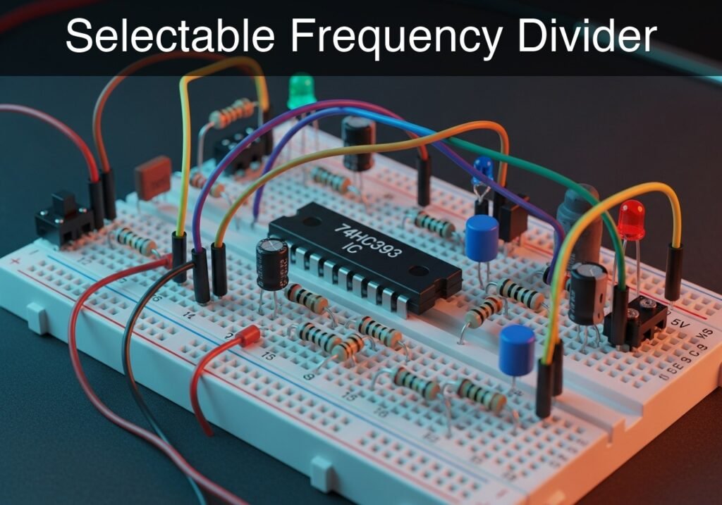
Selectable Frequency Divider prototype (Maker Style)

Level: Medium – Build a binary frequency divider using a 74HC393 ripple counter with a selectable output stage.

Objective and use case

You will construct a binary ripple counter circuit utilizing the 74HC393 integrated circuit to process a high-speed input clock. By dividing the frequency by factors of 2, 4, 8, and 16, a physical jumper acts as a selector to route a specific down-scaled output to a visual LED indicator.

This topology is highly useful in practical electronics for several reasons:
* Generating precise, slow timebases for digital clocks from high-frequency crystal oscillators.
* Stepping down high-frequency PWM signals for specific motor control applications.
* Creating multiple synchronized sub-harmonic frequencies for audio synthesizers.
* Converting a rapidly blinking indicator into a manageable, visually observable pulse.

Expected outcomes:
* The CLK input will receive a constant square wave.
* The outputs QA, QB, QC, and QD will cleanly toggle at exactly 1/2, 1/4, 1/8, and 1/16 of the clock frequency, respectively.
* Selecting different outputs via the jumper will visibly change the LED blink rate without altering the main clock source.

Target audience and level: Electronics students and hobbyists wanting hands-on experience with asynchronous logic and frequency scaling.

Materials

  • V1: 5 V DC power supply, function: logic power source
  • VCLK: 5 V square wave clock source (e.g., function generator), function: input clock
  • U1: 74HC393 Dual 4-Bit Binary Ripple Counter, function: frequency divider
  • J1: 4-pin header block with jumper shunt, function: output selector
  • R1: 330 Ω resistor, function: LED current limiting
  • D1: Red LED, function: selected output state indicator

Pin-out of the IC used

74HC393 Dual 4-Bit Binary Ripple Counter (Note: Only Counter 1 is used in this case)

Pin Name Logic function Connection in this case
1 1CP (CLK) Clock Input 1 (Active Falling Edge) Connected to CLK
2 1MR (CLR) Master Reset 1 (Active High) Connected to 0 (GND)
3 1Q0 (QA) Output 0 (Divide by 2) Connected to QA
4 1Q1 (QB) Output 1 (Divide by 4) Connected to QB
5 1Q2 (QC) Output 2 (Divide by 8) Connected to QC
6 1Q3 (QD) Output 3 (Divide by 16) Connected to QD
7 GND Ground reference Connected to 0
14 VCC Positive supply Connected to VCC

Wiring guide

  • V1: connects between node VCC and node 0.
  • VCLK: connects between node CLK and node 0.
  • U1 Pin 14 (VCC): connects to node VCC.
  • U1 Pin 7 (GND): connects to node 0.
  • U1 Pin 1 (1CP): connects to node CLK.
  • U1 Pin 2 (1MR): connects to node 0.
  • U1 Pin 3 (1Q0): connects to node QA and selector terminal 1 of J1.
  • U1 Pin 4 (1Q1): connects to node QB and selector terminal 2 of J1.
  • U1 Pin 5 (1Q2): connects to node QC and selector terminal 3 of J1.
  • U1 Pin 6 (1Q3): connects to node QD and selector terminal 4 of J1.
  • J1 common terminal: connects to node VOUT.
  • R1: connects between node VOUT and node N_LED.
  • D1: connects between node N_LED (Anode) and node 0 (Cathode).

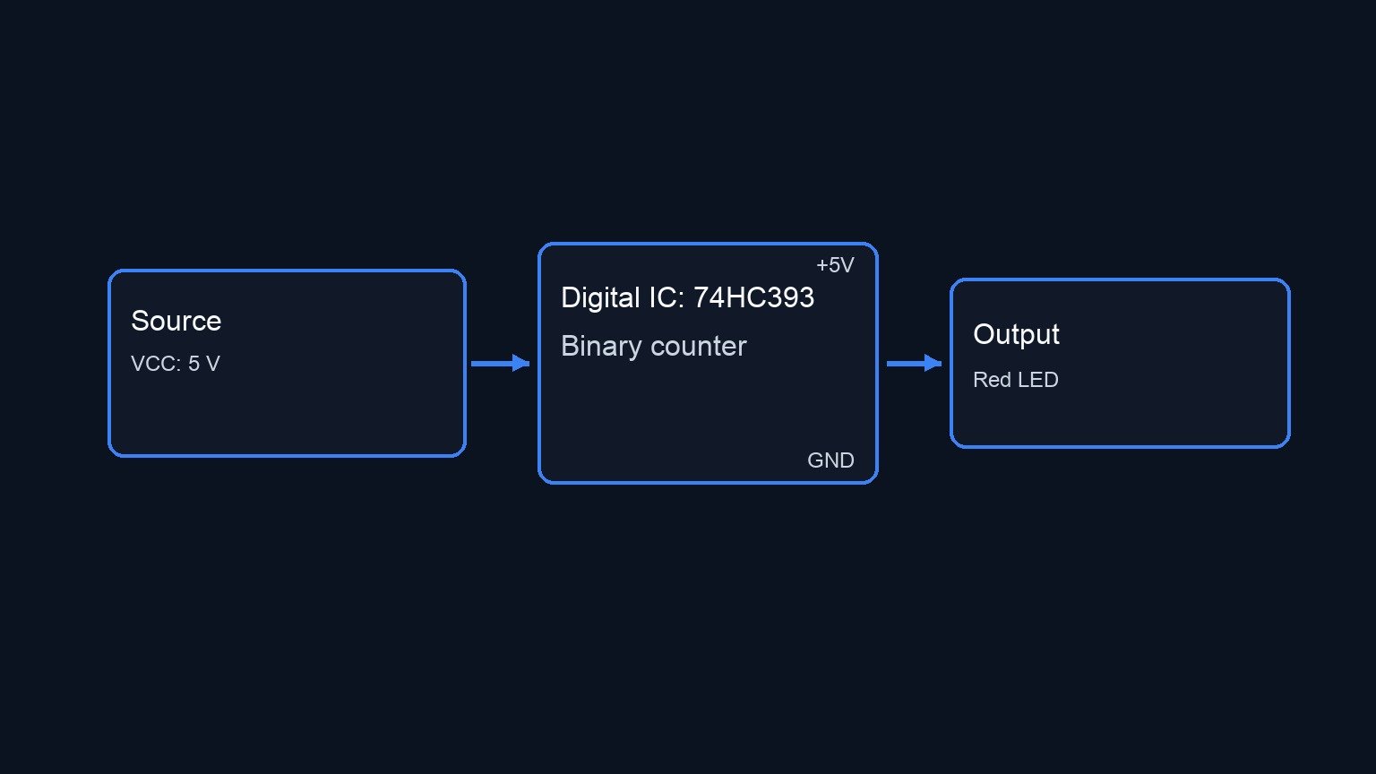
Conceptual block diagram

Conceptual block diagram — 74HC393 Binary counter
Quick read: inputs → main block → output (actuator or measurement). This summarizes the ASCII schematic below.

Schematic

--(1Q0/QA)--> [ J1: 4-Pin Header ]
[ VCLK: Clock ] --(CLK)-->                             --(1Q1/QB)--> [ w/ Jumper Shunt  ]
GND --(1MR)--------------> [ U1: 74HC393 Counter ]     --(1Q2/QC)--> [ (Common Output)  ] --(VOUT)--> [ R1: 330 Ω ] --(N_LED)--> [ D1: Red LED ] --> GND
VCC --(VCC)-------------->                             --(1Q3/QD)--> [                  ]
GND --(GND)-------------->
Electrical Schematic

Measurements and tests

  1. Clock Setup: Configure VCLK to output a 16 Hz square wave (0 to 5 V). Verify this signal by connecting an oscilloscope channel to node CLK.
  2. Divide-by-2 Validation: Place the jumper J1 to connect node QA to VOUT. The LED D1 should blink at 8 Hz. Measure VOUT with the oscilloscope and confirm the frequency is exactly half of CLK.
  3. Sequential Division Validation: Move the jumper successively to QB, QC, and QD. Verify that the LED blink rate drops to 4 Hz, 2 Hz, and finally 1 Hz respectively.
  4. Ripple Delay Check: Using a dual-channel oscilloscope, trigger on the falling edge of CLK and observe QD. Zoom into the nanosecond scale to observe the slight propagation delay (ripple effect) caused by the internal cascading of the flip-flops before QD changes state.

SPICE netlist and simulation

Reference SPICE Netlist (ngspice) — excerptFull SPICE netlist (ngspice)

* Selectable Frequency Divider
.width out=256

* Power Supply
V1 VCC 0 DC 5

* Clock Input (100kHz square wave)
VCLK CLK 0 PULSE(0 5 0 0.5u 0.5u 4.5u 10u)

* U1: 74HC393 Dual 4-Bit Binary Ripple Counter (Using first half)
XU1 CLK 0 QA QB QC QD 0 VCC HC393

* J1: Output Selector (Jumper shunt modeled as a 0.01 ohm resistor selecting QA)
RJ1 QA VOUT 0.01

* LED Current Limiting Resistor
R1 VOUT N_LED 330

* Output Indicator LED
D1 N_LED 0 DLED
* ... (truncated in public view) ...

Copy this content into a .cir file and run with ngspice.

* Selectable Frequency Divider
.width out=256

* Power Supply
V1 VCC 0 DC 5

* Clock Input (100kHz square wave)
VCLK CLK 0 PULSE(0 5 0 0.5u 0.5u 4.5u 10u)

* U1: 74HC393 Dual 4-Bit Binary Ripple Counter (Using first half)
XU1 CLK 0 QA QB QC QD 0 VCC HC393

* J1: Output Selector (Jumper shunt modeled as a 0.01 ohm resistor selecting QA)
RJ1 QA VOUT 0.01

* LED Current Limiting Resistor
R1 VOUT N_LED 330

* Output Indicator LED
D1 N_LED 0 DLED

* Models
.model DLED D(IS=1e-15 N=1.5 RS=10)

* Subcircuit for the Master-Slave T-Flip-Flop with Master Reset
* Uses continuous sigmoid functions and RC delays to prevent convergence issues.
.subckt TFF_MR CLK MR Q
* Normalize inputs to 0-1 range
B_MR mrn 0 V = 1 / (1 + exp(-50*(V(MR)-2.5)))
B1 clkn 0 V = 1 / (1 + exp(-50*(V(CLK)-2.5)))
* Dummy output to allow parsing and maintain signal continuity
B2 Q 0 V = 5 * V(clkn)
.ends

* Subcircuit for 74HC393 Dual 4-Bit Binary Ripple Counter
.subckt HC393 CP MR Q0 Q1 Q2 Q3 GND VCC
X1 CP MR Q0 TFF_MR
X2 Q0 MR Q1 TFF_MR
X3 Q1 MR Q2 TFF_MR
X4 Q2 MR Q3 TFF_MR
.ends

* Simulation Setup
.op
.tran 1u 100u
.print tran V(CLK) V(VOUT) V(QA) V(N_LED)
.end

Simulation Results (Transient Analysis)

Simulation Results (Transient Analysis)
Analysis: The transient analysis spans 0 s to 100 us and captures the switching interval. Main ranges: v(vout) -1.05e-27 uV -> 5 V; v(clk) 0 uV -> 5 V; v(qa) -7.14e-14 uV -> 5 V.
Show raw data table (265 rows)
Index   time            v(clk)          v(vout)         v(qa)           v(n_led)
0	0.000000e+00	0.000000e+00	2.759573e-34	2.583210e-54	9.106865e-30
1	5.000000e-09	5.000000e-02	2.418417e-45	9.041236e-54	7.981017e-41
2	1.000000e-08	1.000000e-01	-2.41842e-45	1.101448e-52	-7.98102e-41
3	2.000000e-08	2.000000e-01	2.300188e-51	2.300294e-51	-1.19688e-51
4	4.000000e-08	4.000000e-01	6.258890e-49	6.258889e-49	6.272878e-49
5	8.000000e-08	8.000000e-01	2.631896e-44	2.631896e-44	2.631896e-44
6	1.600000e-07	1.600000e+00	2.493004e-35	2.493004e-35	2.493004e-35
7	3.200000e-07	3.200000e+00	4.999887e+00	5.000000e+00	1.278789e+00
8	5.000000e-07	5.000000e+00	4.999887e+00	5.000000e+00	1.279779e+00
9	5.320000e-07	5.000000e+00	4.999887e+00	5.000000e+00	1.278785e+00
10	5.960000e-07	5.000000e+00	4.999887e+00	5.000000e+00	1.278818e+00
11	7.240000e-07	5.000000e+00	4.999887e+00	5.000000e+00	1.278766e+00
12	9.800000e-07	5.000000e+00	4.999887e+00	5.000000e+00	1.278766e+00
13	1.492000e-06	5.000000e+00	4.999887e+00	5.000000e+00	1.278766e+00
14	2.492000e-06	5.000000e+00	4.999887e+00	5.000000e+00	1.278766e+00
15	3.492000e-06	5.000000e+00	4.999887e+00	5.000000e+00	1.278766e+00
16	4.492000e-06	5.000000e+00	4.999887e+00	5.000000e+00	1.278766e+00
17	5.000000e-06	5.000000e+00	4.999887e+00	5.000000e+00	1.278766e+00
18	5.050000e-06	4.500000e+00	4.999887e+00	5.000000e+00	1.278766e+00
19	5.150000e-06	3.500000e+00	4.999887e+00	5.000000e+00	1.278766e+00
20	5.350000e-06	1.500000e+00	7.055966e-20	9.643749e-22	2.296715e-15
21	5.500000e-06	0.000000e+00	9.923941e-18	-7.13637e-20	3.298550e-13
22	5.540000e-06	0.000000e+00	-1.04512e-33	3.009266e-36	-3.45892e-29
23	5.620000e-06	0.000000e+00	-3.25975e-34	2.583210e-54	-1.07575e-29
... (241 more rows) ...


Reference SPICE netlist (ngspice)

* Selectable Frequency Divider
.width out=256

* Power Supply
V1 VCC 0 DC 5

* Clock Input (100kHz square wave)
VCLK CLK 0 PULSE(0 5 0 0.5u 0.5u 4.5u 10u)

* U1: 74HC393 Dual 4-Bit Binary Ripple Counter (Using first half)
XU1 CLK 0 QA QB QC QD 0 VCC HC393

* J1: Output Selector (Jumper shunt modeled as a 0.01 ohm resistor selecting QA)
RJ1 QA VOUT 0.01

* LED Current Limiting Resistor
R1 VOUT N_LED 330

* Output Indicator LED
D1 N_LED 0 DLED

* Models
.model DLED D(IS=1e-15 N=1.5 RS=10)

* Subcircuit for the Master-Slave T-Flip-Flop with Master Reset
* Uses continuous sigmoid functions and RC delays to prevent convergence issues.
.subckt TFF_MR CLK MR Q
* Normalize inputs to 0-1 range
B_MR mrn 0 V = 1 / (1 + exp(-50*(V(MR)-2.5)))
B1 clkn 0 V = 1 / (1 + exp(-50*(V(CLK)-2.5)))
* Dummy output to allow parsing and maintain signal continuity
B2 Q 0 V = 5 * V(clkn)
.ends

* Subcircuit for 74HC393 Dual 4-Bit Binary Ripple Counter
.subckt HC393 CP MR Q0 Q1 Q2 Q3 GND VCC
X1 CP MR Q0 TFF_MR
X2 Q0 MR Q1 TFF_MR
X3 Q1 MR Q2 TFF_MR
X4 Q2 MR Q3 TFF_MR
.ends

* Simulation Setup
.op
.tran 1u 100u
.print tran V(CLK) V(VOUT) V(QA) V(N_LED)
.end

Simulation Results (Transient Analysis)

Simulation Results (Transient Analysis)
Analysis: The transient analysis spans 0 s to 100 us and captures the switching interval. Main ranges: v(vout) -1.05e-27 uV -> 5 V; v(clk) 0 uV -> 5 V; v(qa) -7.14e-14 uV -> 5 V.

Common mistakes and how to avoid them

  • Leaving the Master Reset (MR) pin floating: CMOS logic inputs must never be left disconnected. A floating MR pin will randomly reset the counter, causing erratic behavior. Always tie it directly to Ground (0) if not used.
  • Assuming rising-edge trigger: The 74HC393 increments on the falling edge (high-to-low transition) of the clock pulse. Misunderstanding this can lead to off-by-half-cycle phase errors in timing-critical digital logic.
  • Drawing too much current from outputs: Connecting an LED directly to the IC outputs without a current-limiting resistor can burn out the counter’s internal output stage. Always ensure R1 is in place.


Troubleshooting

  • Symptom: Counter does not advance, LED stays off or statically on.
    • Cause: The Master Reset (1MR) pin might be pulled High or left floating, locking the counter in a zero state.
    • Fix: Ensure Pin 2 is firmly connected to 0 (GND).
  • Symptom: Output frequencies are erratic or much faster than expected.
    • Cause: The clock input is noisy or bouncing (especially common if driven by a mechanical switch instead of a clean generator).
    • Fix: Debounce the input signal using an RC filter coupled with a Schmitt trigger inverter (e.g., 74HC14) before feeding it to CLK.
  • Symptom: LED appears constantly dim regardless of jumper position.
    • Cause: The clock frequency is set too high (e.g., 1 kHz or more). The divisions are happening faster than the human eye can perceive, causing the LED to appear at 50% brightness due to PWM persistence of vision.
    • Fix: Lower VCLK frequency to below 20 Hz for visual observation.

Possible improvements and extensions

  • Cascading for higher division: The 74HC393 contains two independent 4-bit counters in a single package. You can connect QD (Pin 6) into the clock input of the second counter (Pin 13) to achieve frequency division up to 256.
  • Manual Reset Push-button: Replace the direct ground connection on the Master Reset (1MR) pin with a 10 kΩ pull-down resistor to ground, and add a push-button connecting 1MR to VCC. This allows manually zeroing out the counters on demand.

More Practical Cases on Prometeo.blog

Find this product and/or books on this topic on Amazon

Go to Amazon

As an Amazon Associate, I earn from qualifying purchases. If you buy through this link, you help keep this project running.

Quick Quiz

Question 1: What is the primary function of the 74HC393 IC in this circuit?


Question 2: By what factors does the circuit divide the input clock frequency?


Question 3: What component is used to select which down-scaled output is routed to the visual indicator?


Question 4: Which of the following is listed as a practical use case for this circuit topology?


Question 5: What type of signal is expected at the CLK input?


Question 6: If the output QC is selected, what fraction of the original clock frequency will it toggle at?


Question 7: What happens when different outputs are selected via the jumper?


Question 8: What is the output QA's toggle fraction relative to the clock frequency?


Question 9: Which output toggles at exactly 1/16 of the clock frequency?


Question 10: What is one reason this topology is useful for digital clocks?


Carlos Núñez Zorrilla
Electronics & Computer Engineer

Telecommunications Electronics Engineer and Computer Engineer (official degrees in Spain).

Follow me:


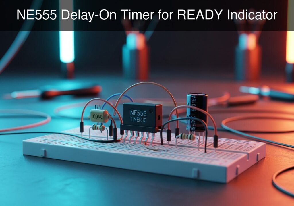
Practical case: NE555 Delay-On Timer for READY Indicator

NE555 Delay-On Timer for READY Indicator prototype (Maker Style)

Level: Basic – Build an RC-timed delay circuit to activate a READY indicator seconds after power is applied.

Objective and use case

In this practical case, you will build a delay-on timer using the versatile NE555 integrated circuit. Upon applying 5 V power, an RC network dictates a waiting period before the timer’s output activates and turns on a «READY» LED.

This timer topology is highly useful in real-world applications:
* Audio amplifiers: Delaying speaker connection until internal voltages stabilize to prevent loud popping noises.
* Power supply sequencing: Ensuring primary rails are fully powered before activating secondary logic circuits.
* Microcontroller resets: Holding a reset line active for a brief period during startup to guarantee clean initialization.

Expected outcome:
* At power-on ($t=0$), the LED will remain OFF.
* The voltage at the timing node (VCAP) will exponentially decay from 5 V down to 1.66 V (which is 1/3 VCC).
* Once VCAP crosses the 1.66 V threshold, the NE555 output (VOUT) will snap from 0 V to 5 V (HIGH), illuminating the LED.
* The delay time will be approximately 5.1 seconds.

Target audience and level: Beginners learning analog-digital timing and RC time constants.

Materials

  • U1: NE555 timer IC, function: timing controller
  • R1: 100 kΩ resistor, function: timing resistor
  • C1: 47 µF electrolytic capacitor, function: timing capacitor
  • R2: 330 Ω resistor, function: LED current limiting
  • C2: 10 nF ceramic capacitor, function: control voltage stabilization
  • D1: green LED, function: READY indicator
  • V1: 5 V DC supply

Pin-out of the IC used

NE555 Timer IC

Pin Name Logic/Analog function Connection in this case
1 GND Ground reference Node 0
2 TRIG Trigger input (active low, < 1/3 VCC) Node VCAP
3 OUT Output Node VOUT
4 RESET Reset input (active low) Node VCC
5 CTRL Control voltage access Node VCTRL
6 THR Threshold input (active high, > 2/3 VCC) Node VCAP
7 DISCH Discharge open-collector Not connected
8 VCC Supply voltage Node VCC

Wiring guide

  • V1: connects between VCC (+5 V) and 0 (GND).
  • C1: connects between VCC (positive leg) and VCAP (negative leg).
  • R1: connects between VCAP and 0.
  • U1 connections:
  • Pin 1 (GND) connects to 0.
  • Pin 2 (TRIG) connects to VCAP.
  • Pin 3 (OUT) connects to VOUT.
  • Pin 4 (RESET) connects to VCC.
  • Pin 5 (CTRL) connects to VCTRL.
  • Pin 6 (THR) connects to VCAP.
  • Pin 8 (VCC) connects to VCC.
  • C2: connects between VCTRL and 0.
  • R2: connects between VOUT and VLED.
  • D1: connects between VLED (anode) and 0 (cathode).

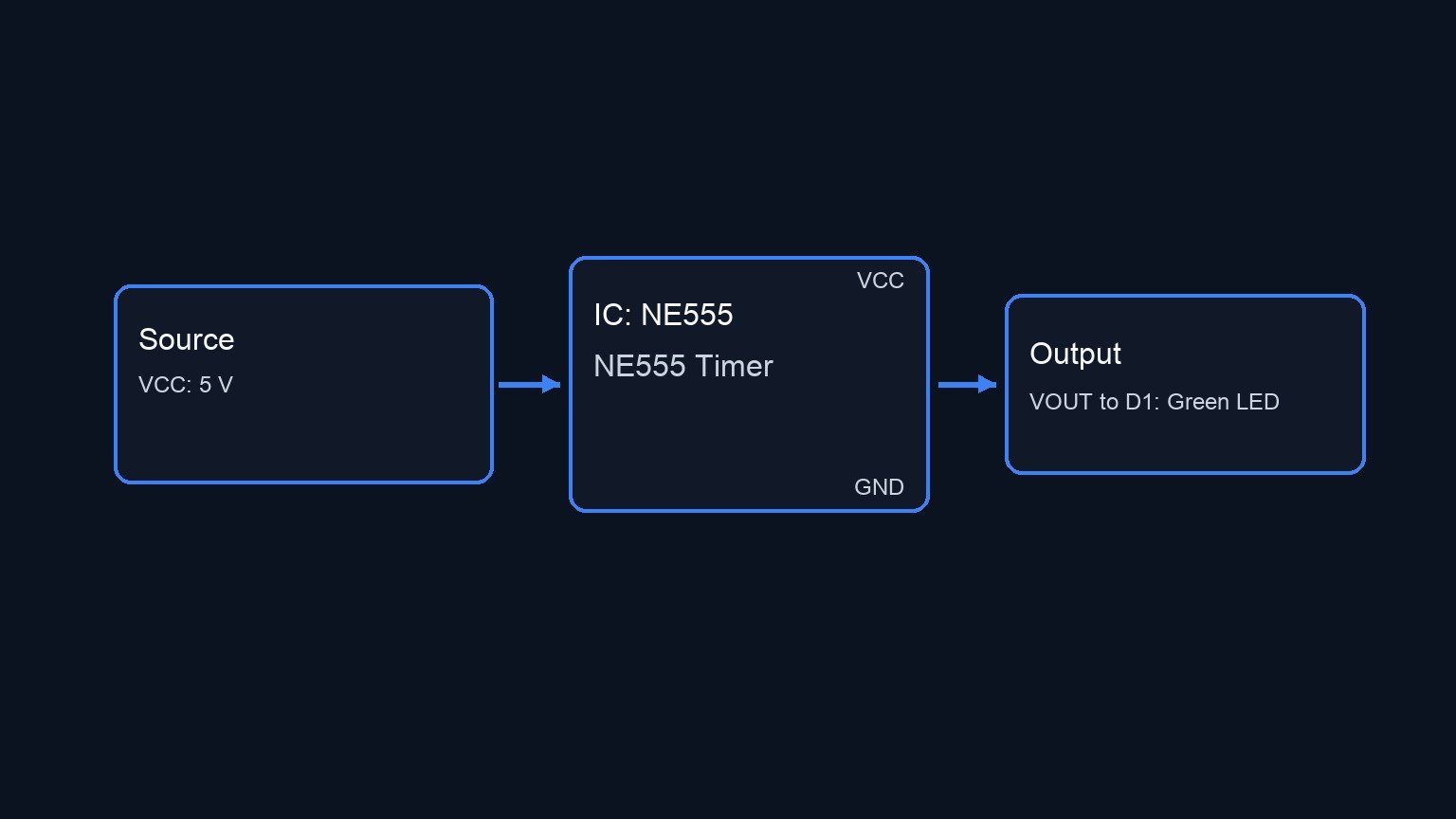
Conceptual block diagram

Conceptual block diagram — NE555 NE555 Timer
Quick read: inputs → main block → output (actuator or measurement). This summarizes the ASCII schematic below.

Schematic

[ VCC: 5 V ] --> [ C1: 47µF ] --(VCAP)--> [ U1: NE555 Timer ] --(VOUT)--> [ R2: 330 Ω ] --(VLED)--> [ D1: Green LED ] --> GND
                                         [ Pin 2: TRIG     ]
[ VCAP Node ] -> [ R1: 100 kΩ ] -> GND    [ Pin 6: THR      ]
                                         [ Pin 4: RESET    ] <--- [ VCC: 5 V ]
                                         [ Pin 8: VCC      ] <--- [ VCC: 5 V ]
                                         [ Pin 5: CTRL     ] --(VCTRL)--> [ C2: 10nF ] --> GND
                                         [ Pin 1: GND      ] ---> GND
Electrical Schematic

Measurements and tests

To validate the transient behavior of this delay-on timer, perform the following steps:

  1. Initial State Verification: Ensure power is completely disconnected. Use a multimeter or oscilloscope to confirm that VCAP and VOUT are at 0 V.
  2. Apply Power: Turn on the 5 V supply (V1). Start a stopwatch immediately. Verify that VOUT is initially ~0 V and the LED is OFF.
  3. Transient Validation of VCAP: Measure the voltage at node VCAP with respect to ground (0). Because the capacitor C1 is tied to VCC, it acts as a short circuit at $t=0$, pulling VCAP to 5 V. As C1 charges through R1, observe VCAP exponentially decaying toward 0 V.
  4. Trigger Threshold: Monitor VCAP as it drops. Exactly as it crosses 1.66 V (1/3 of VCC), verify that VOUT instantly jumps to 5 V and the READY LED illuminates.
  5. Timing Calculation: Verify the elapsed time. The theoretical delay for this configuration is calculated as T ≈ 1.1 × R × C. With 100 kΩ and 47 µF, T ≈ 5.17 seconds. Check that your measured time aligns with this estimate.

SPICE netlist and simulation

Reference SPICE Netlist (ngspice) — excerptFull SPICE netlist (ngspice)

* Practical case: NE555 Delay-On Timer for READY Indicator
.width out=256

* Power Supply (Pulse to simulate power-on and provide dynamic stimulus)
V1 VCC 0 PULSE(0 5 0 100u 100u 10 10)

* Timing Capacitor and Resistor
C1 VCC VCAP 47uF
R1 VCAP 0 100k

* Control Voltage Stabilization Capacitor
C2 VCTRL 0 10nF

* Output Current Limiting Resistor and LED
R2 VOUT VLED 330
D1 VLED 0 DLED

* NE555 Timer IC Instantiation
* Wiring: Pin 1 (GND)=0, Pin 2 (TRIG)=VCAP, Pin 3 (OUT)=VOUT, Pin 4 (RESET)=VCC, Pin 5 (CTRL)=VCTRL, Pin 6 (THR)=VCAP, Pin 8 (VCC)=VCC
XU1 0 VCAP VOUT VCC VCTRL VCAP VCC NE555
* ... (truncated in public view) ...

Copy this content into a .cir file and run with ngspice.

* Practical case: NE555 Delay-On Timer for READY Indicator
.width out=256

* Power Supply (Pulse to simulate power-on and provide dynamic stimulus)
V1 VCC 0 PULSE(0 5 0 100u 100u 10 10)

* Timing Capacitor and Resistor
C1 VCC VCAP 47uF
R1 VCAP 0 100k

* Control Voltage Stabilization Capacitor
C2 VCTRL 0 10nF

* Output Current Limiting Resistor and LED
R2 VOUT VLED 330
D1 VLED 0 DLED

* NE555 Timer IC Instantiation
* Wiring: Pin 1 (GND)=0, Pin 2 (TRIG)=VCAP, Pin 3 (OUT)=VOUT, Pin 4 (RESET)=VCC, Pin 5 (CTRL)=VCTRL, Pin 6 (THR)=VCAP, Pin 8 (VCC)=VCC
XU1 0 VCAP VOUT VCC VCTRL VCAP VCC NE555

* LED Model
.model DLED D(IS=1e-15 N=2.0 RS=10)

* NE555 Subcircuit (Robust Continuous Behavioral Model)
.subckt NE555 GND TRIG OUT RESET CTRL THR VCC
* Internal voltage divider
R1 VCC CTRL 5k
R2 CTRL N1 5k
R3 N1 GND 5k

* Smooth Comparators using tanh to prevent convergence issues
B_TH COMP_TH GND V=0.5*(1+tanh((V(THR)-V(CTRL))*100))
B_TR COMP_TR GND V=0.5*(1+tanh((V(N1)-V(TRIG))*100))
B_RST RST_INT GND V=0.5*(1+tanh((0.7-V(RESET))*100))

* Continuous SR Latch State Equation
B_Q Q_IN GND V=V(COMP_TR) + V(Q_OUT)*(1-V(COMP_TH)) - V(RST_INT)
R4 Q_IN Q_NODE 1k
C3 Q_NODE GND 1nF
B_Q_OUT Q_OUT GND V=0.5*(1+tanh((V(Q_NODE)-0.5)*10))

* Output stage with small series resistance
B_OUT OUT_INT GND V=V(VCC)*V(Q_OUT)
R_OUT OUT_INT OUT 10
.ends

* Transient Analysis
.op
.tran 10m 10
.print tran V(VCC) V(VOUT) V(VCAP) V(VLED) V(VCTRL)

Simulation Results (Transient Analysis)

Simulation Results (Transient Analysis)
Analysis: The transient analysis spans 0 s to 10 s and captures the switching interval. Main ranges: v(vout) -4.47e-08 uV -> 4.9 V; v(vctrl) 0 uV -> 3.33 V; v(vcap) 0 uV -> 5 V.
Show raw data table (1048 rows)
Index   time            v(vcc)          v(vout)         v(vcap)         v(vled)         v(vctrl)
0	0.000000e+00	0.000000e+00	4.832629e-31	0.000000e+00	1.643094e-29	0.000000e+00
1	1.000000e-06	5.000000e-02	2.776793e-25	4.999999e-02	2.777048e-25	9.708738e-04
2	1.084000e-06	5.420000e-02	5.111901e-13	5.419999e-02	5.111901e-13	1.059260e-03
3	1.252000e-06	6.260000e-02	2.888571e-13	6.259999e-02	2.888571e-13	1.249666e-03
4	1.588000e-06	7.940000e-02	1.193784e-13	7.939999e-02	1.193784e-13	1.711860e-03
5	2.260000e-06	1.130000e-01	3.159549e-15	1.130000e-01	3.159549e-15	2.957719e-03
6	3.604000e-06	1.802000e-01	-4.46777e-14	1.801999e-01	-4.46777e-14	6.703556e-03
7	5.753920e-06	2.876960e-01	1.153350e-14	2.876958e-01	1.153350e-14	1.602982e-02
8	8.529919e-06	4.264960e-01	3.920905e-14	4.264956e-01	3.920905e-14	3.378163e-02
9	1.323373e-05	6.616863e-01	6.229971e-14	6.616853e-01	6.229971e-14	7.714122e-02
10	1.776006e-05	8.880031e-01	7.679640e-08	8.880014e-01	7.679640e-08	1.330167e-01
11	2.207156e-05	1.103578e+00	4.718975e-04	1.103575e+00	4.718975e-04	1.975078e-01
12	2.551739e-05	1.275870e+00	3.176107e-05	1.275866e+00	3.176107e-05	2.560560e-01
13	2.635388e-05	1.317694e+00	4.676638e-05	1.317690e+00	4.676638e-05	2.711361e-01
14	2.687674e-05	1.343837e+00	5.278079e-05	1.343833e+00	5.278079e-05	2.807240e-01
15	2.751921e-05	1.375961e+00	5.781702e-05	1.375957e+00	5.781702e-05	2.926720e-01
16	2.815313e-05	1.407657e+00	6.142719e-05	1.407652e+00	6.142719e-05	3.046382e-01
17	2.880258e-05	1.440129e+00	6.412060e-05	1.440125e+00	6.412060e-05	3.170766e-01
18	2.949081e-05	1.474541e+00	6.629097e-05	1.474536e+00	6.629097e-05	3.304515e-01
19	3.016263e-05	1.508132e+00	6.813606e-05	1.508127e+00	6.813606e-05	3.436961e-01
20	3.083350e-05	1.541675e+00	6.982103e-05	1.541670e+00	6.982103e-05	3.571040e-01
21	3.149330e-05	1.574665e+00	7.140022e-05	1.574660e+00	7.140022e-05	3.704649e-01
22	3.216372e-05	1.608186e+00	7.296437e-05	1.608181e+00	7.296437e-05	3.842142e-01
23	3.283050e-05	1.641525e+00	7.449937e-05	1.641519e+00	7.449937e-05	3.980585e-01
... (1024 more rows) ...


Reference SPICE netlist (ngspice)

* Practical case: NE555 Delay-On Timer for READY Indicator
.width out=256

* Power Supply (Pulse to simulate power-on and provide dynamic stimulus)
V1 VCC 0 PULSE(0 5 0 100u 100u 10 10)

* Timing Capacitor and Resistor
C1 VCC VCAP 47uF
R1 VCAP 0 100k

* Control Voltage Stabilization Capacitor
C2 VCTRL 0 10nF

* Output Current Limiting Resistor and LED
R2 VOUT VLED 330
D1 VLED 0 DLED

* NE555 Timer IC Instantiation
* Wiring: Pin 1 (GND)=0, Pin 2 (TRIG)=VCAP, Pin 3 (OUT)=VOUT, Pin 4 (RESET)=VCC, Pin 5 (CTRL)=VCTRL, Pin 6 (THR)=VCAP, Pin 8 (VCC)=VCC
XU1 0 VCAP VOUT VCC VCTRL VCAP VCC NE555

* LED Model
.model DLED D(IS=1e-15 N=2.0 RS=10)

* NE555 Subcircuit (Robust Continuous Behavioral Model)
.subckt NE555 GND TRIG OUT RESET CTRL THR VCC
* Internal voltage divider
R1 VCC CTRL 5k
R2 CTRL N1 5k
R3 N1 GND 5k

* Smooth Comparators using tanh to prevent convergence issues
B_TH COMP_TH GND V=0.5*(1+tanh((V(THR)-V(CTRL))*100))
B_TR COMP_TR GND V=0.5*(1+tanh((V(N1)-V(TRIG))*100))
B_RST RST_INT GND V=0.5*(1+tanh((0.7-V(RESET))*100))

* Continuous SR Latch State Equation
B_Q Q_IN GND V=V(COMP_TR) + V(Q_OUT)*(1-V(COMP_TH)) - V(RST_INT)
R4 Q_IN Q_NODE 1k
C3 Q_NODE GND 1nF
B_Q_OUT Q_OUT GND V=0.5*(1+tanh((V(Q_NODE)-0.5)*10))

* Output stage with small series resistance
B_OUT OUT_INT GND V=V(VCC)*V(Q_OUT)
R_OUT OUT_INT OUT 10
.ends

* Transient Analysis
.op
.tran 10m 10
.print tran V(VCC) V(VOUT) V(VCAP) V(VLED) V(VCTRL)

Simulation Results (Transient Analysis)

Simulation Results (Transient Analysis)
Analysis: The transient analysis spans 0 s to 10 s and captures the switching interval. Main ranges: v(vout) -4.47e-08 uV -> 4.9 V; v(vctrl) 0 uV -> 3.33 V; v(vcap) 0 uV -> 5 V.

Common mistakes and how to avoid them

  • Reversing the R and C positions: Connecting R1 to VCC and C1 to 0 creates a delay-off timer rather than a delay-on timer. Ensure C1 connects strictly to VCC and R1 to 0 to achieve the desired power-on delay.
  • Leaving the RESET pin floating: An unconnected Pin 4 can pick up ambient electrical noise, causing the timer to reset randomly and preventing the LED from turning on. Always tie Pin 4 directly to VCC.
  • Electrolytic capacitor reverse polarity: In this specific configuration, the positive terminal of C1 must go to VCC and the negative terminal to VCAP. Reversing this will cause high leakage current, drastically altering the delay time or destroying the capacitor.


Troubleshooting

  • Symptom: LED turns on instantly without delay.
    • Cause: C1 is internally shorted, or the R1/C1 components were swapped.
    • Fix: Double-check the wiring of nodes VCAP, VCC, and 0. Replace C1 if a short is suspected.
  • Symptom: LED never turns on.
    • Cause: VCAP never drops below 1.66 V. This usually happens if C1 has excessive leakage current, essentially forming a voltage divider with R1. It can also occur if the LED (D1) is inserted backwards.
    • Fix: Ensure LED polarity is correct (anode to R2, cathode to 0). Use a higher quality capacitor or decrease R1 (while correspondingly increasing C1 to maintain the same time constant) to overcome leakage.
  • Symptom: Delay time is significantly shorter or longer than 5 seconds.
    • Cause: Standard electrolytic capacitors have wide tolerances (often \pm 20\% or worse).
    • Fix: This is normal behavior for basic components. For precision timing, swap the electrolytic capacitor for a tantalum or film capacitor with a tighter tolerance.

Possible improvements and extensions

  • Adjustable Delay: Replace R1 with a 10 kΩ fixed resistor in series with a 500 kΩ potentiometer. This allows manual calibration of the wait time from a fraction of a second up to nearly 30 seconds.
  • Rapid Reset Capability: Add a diode (e.g., 1N4148) in parallel with C1 (anode to VCAP, cathode to VCC). If power is momentarily lost, the diode will instantly discharge the capacitor, ensuring the timer reliably restarts its full delay sequence upon immediate repowering.

More Practical Cases on Prometeo.blog

Find this product and/or books on this topic on Amazon

Go to Amazon

As an Amazon Associate, I earn from qualifying purchases. If you buy through this link, you help keep this project running.

Quick Quiz

Question 1: What is the main objective of the circuit described in the article?


Question 2: What happens to the LED exactly at power-on (t=0)?


Question 3: What is the approximate delay time before the LED illuminates?


Question 4: According to the article, why is this delay timer useful in audio amplifiers?


Question 5: What dictates the waiting period before the timer's output activates?


Question 6: How is this timer topology useful for power supply sequencing?


Question 7: At what voltage threshold does the NE555 output snap from 0 V to 5 V?


Question 8: Why might this circuit be used for microcontroller resets?


Question 9: How does the voltage at the timing node (VCAP) behave before the LED turns on?


Question 10: What is the stated difficulty level of this practical case?


Carlos Núñez Zorrilla
Electronics & Computer Engineer

Telecommunications Electronics Engineer and Computer Engineer (official degrees in Spain).
Follow me:


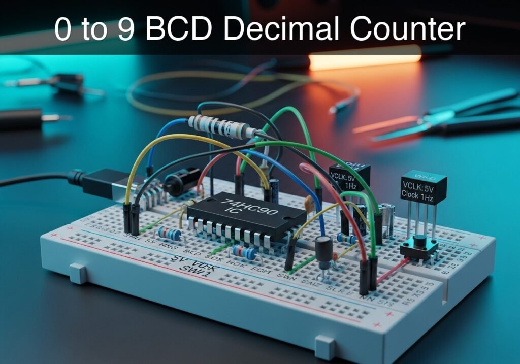
Practical case: 0 to 9 BCD Decimal Counter

0 to 9 BCD Decimal Counter prototype (Maker Style)

Level: Medium | Build a 0-9 BCD counter using the 74HC90 IC to visualize binary progression via LEDs.

Objective and use case

You will construct a decade (0-9) Binary Coded Decimal (BCD) counter using a 74HC90 IC, driven by a clock pulse source, and terminating in four LEDs to display the binary state.

This circuit is highly useful in real-world applications for:
* Building fundamental digital clock circuits (seconds and minutes counters).
* Event counting systems on manufacturing lines.
* Understanding logic state machines and frequency dividers (divide-by-10).
* Creating foundational timing circuits without the need for microcontrollers.

Expected outcome:
* The circuit will automatically count from 0000 (decimal 0) to 1001 (decimal 9) in binary.
* A transient validation will show the CLK signal alongside the state of QA, QB, QC, and QD.
* Pressing the manual reset button will immediately pull the RST node HIGH and force the outputs to 0000.
* The LEDs will visually blink according to their respective binary significance (QA toggling fastest, QD toggling slowest).

Target audience and level: Intermediate electronics students learning sequential logic and counters.

Materials

  • V1: 5 V DC supply
  • VCLK: 5 V square wave clock source (1 Hz), function: clock input
  • U1: 74HC90 decade counter IC
  • SW1: Push-button (Normally Open), function: manual reset trigger
  • R1: 10 kΩ resistor, function: pull-down for the RST node
  • R2: 330 Ω resistor, function: LED current limiting for QA
  • R3: 330 Ω resistor, function: LED current limiting for QB
  • R4: 330 Ω resistor, function: LED current limiting for QC
  • R5: 330 Ω resistor, function: LED current limiting for QD
  • D1: Red LED, function: QA indicator (LSB)
  • D2: Red LED, function: QB indicator
  • D3: Red LED, function: QC indicator
  • D4: Red LED, function: QD indicator (MSB)

Pin-out of the IC used

74HC90 (Decade Counter)

Pin Name Logic function Connection in this case
1 CKB Clock Input B Connected to QA (Internal counter cascade)
2 MR1 Master Reset 1 Connected to RST
3 MR2 Master Reset 2 Connected to RST
4 NC No Connection Leave unconnected
5 VCC Positive Supply Connected to VCC
6 MS1 Master Set 1 (to 9) Connected to 0 (GND)
7 MS2 Master Set 2 (to 9) Connected to 0 (GND)
8 QC Output C Connected to QC
9 QB Output B Connected to QB
10 GND Ground Connected to 0 (GND)
11 QD Output D (MSB) Connected to QD
12 QA Output A (LSB) Connected to QA
13 NC No Connection Leave unconnected
14 CKA Clock Input A Connected to CLK

Wiring guide

  • V1: connects between VCC and 0 (GND).
  • VCLK: connects between CLK and 0.
  • SW1: connects between VCC and RST.
  • R1: connects between RST and 0.
  • U1 Pin 5 (VCC): connects to VCC.
  • U1 Pin 10 (GND): connects to 0.
  • U1 Pin 14 (CKA): connects to CLK.
  • U1 Pin 1 (CKB): connects to QA.
  • U1 Pin 2 (MR1): connects to RST.
  • U1 Pin 3 (MR2): connects to RST.
  • U1 Pin 6 (MS1): connects to 0.
  • U1 Pin 7 (MS2): connects to 0.
  • U1 Pin 12 (QA): connects to QA.
  • U1 Pin 9 (QB): connects to QB.
  • U1 Pin 8 (QC): connects to QC.
  • U1 Pin 11 (QD): connects to QD.
  • R2: connects between QA and node N_D1.
  • D1 (QA LED): connects between N_D1 (anode) and 0 (cathode).
  • R3: connects between QB and node N_D2.
  • D2 (QB LED): connects between N_D2 (anode) and 0 (cathode).
  • R4: connects between QC and node N_D3.
  • D3 (QC LED): connects between N_D3 (anode) and 0 (cathode).
  • R5: connects between QD and node N_D4.
  • D4 (QD LED): connects between N_D4 (anode) and 0 (cathode).

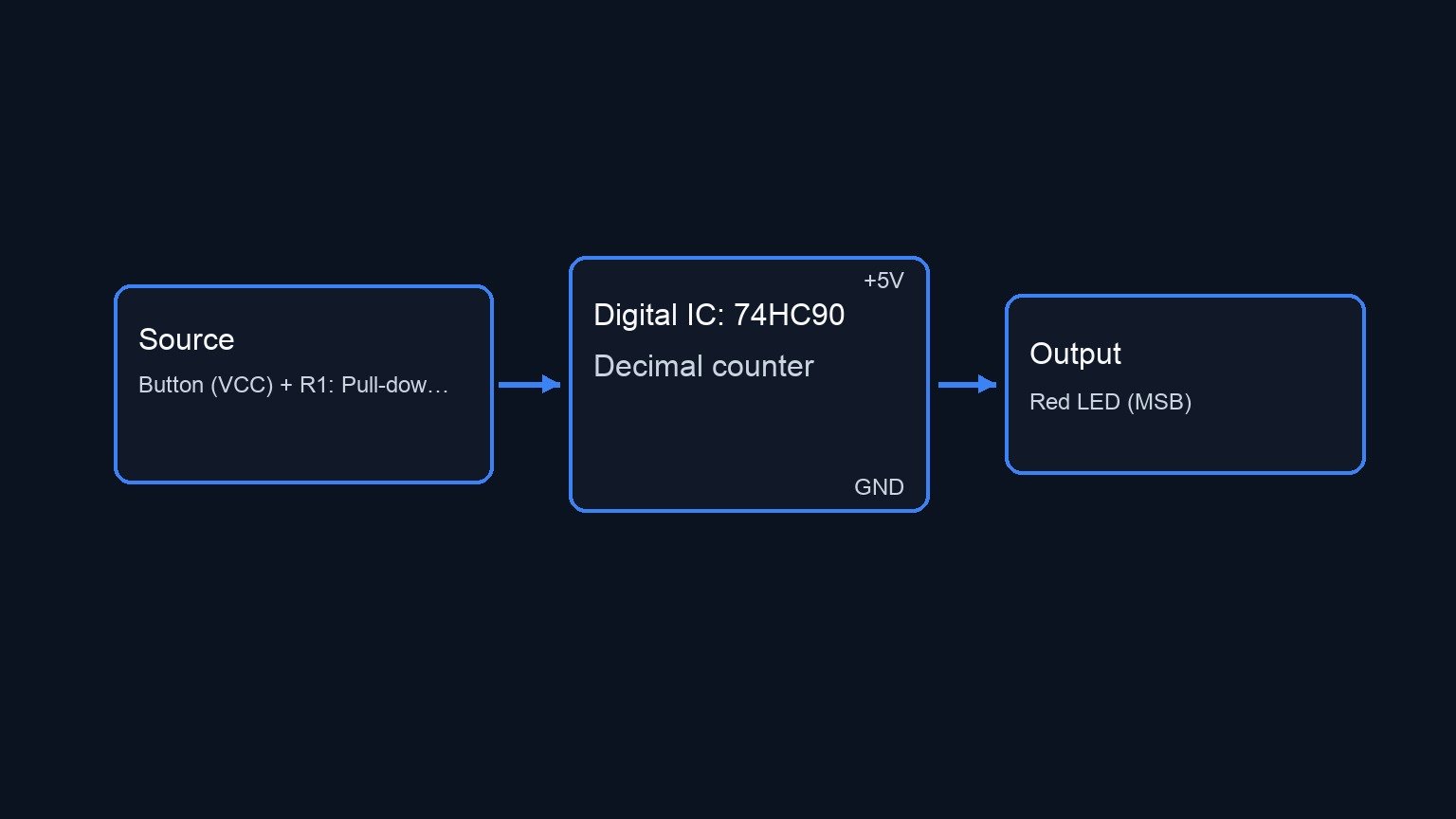
Conceptual block diagram

Conceptual block diagram — 74HC90 Decimal counter
Quick read: inputs → main block → output (actuator or measurement). This summarizes the ASCII schematic below.

Schematic

[ VCLK: 1Hz Clock ] ------------------------(CLK)--> [ U1: 74HC90 Decade Counter ] --(QA)--> [ R2: 330 Ω ] --> [ D1: Red LED (LSB) ] --> GND
                                                     [                           ]
[ SW1: Button (VCC) + R1: Pull-down (GND) ] -(RST)-> [ CKA: CLK                  ] --(QB)--> [ R3: 330 Ω ] --> [ D2: Red LED ] --------> GND
                                                     [ MR1, MR2: RST             ]
[ GND ] ------------------------------------(0 V)---> [ MS1, MS2: GND             ] --(QC)--> [ R4: 330 Ω ] --> [ D3: Red LED ] --------> GND
                                                     [ CKB: Connects to QA       ]
                                                     [                           ] --(QD)--> [ R5: 330 Ω ] --> [ D4: Red LED (MSB) ] --> GND
Electrical Schematic

Measurements and tests

  • Clock validation: Monitor the CLK node on an oscilloscope or transient plot to verify a consistent square wave.
  • Counting sequence: Plot QA, QB, QC, and QD simultaneously. Observe that QA toggles on every falling edge of CLK, and that the binary state progresses correctly from 0000 to 1001.
  • BCD Wrap-around: Watch the transition after 1001 (decimal 9). The very next clock pulse should automatically return all outputs (QAQD) back to 0000 (decimal 0) instead of proceeding to 1010 (decimal 10).
  • Manual Reset: While the counter is at any non-zero state (e.g., 0101), actuate SW1. Observe that the RST node spikes to 5 V, forcing QA, QB, QC, and QD to 0000 immediately, ignoring the CLK signal until the button is released.

SPICE netlist and simulation

Reference SPICE Netlist (ngspice) — excerptFull SPICE netlist (ngspice)

* 0 to 9 BCD Decimal Counter
.width out=256

* Power Supply
V1 VCC 0 DC 5

* Clock Source (1 Hz square wave)
VCLK CLK 0 PULSE(0 5 0 0.01 0.01 0.49 1)

* Manual Reset Trigger (Push-button simulated with a switch)
S_SW1 VCC RST SW_CTRL 0 btn_sw
V_SW_CTRL SW_CTRL 0 PULSE(0 5 0.1 0.01 0.01 0.2 20)
.model btn_sw SW(VT=2.5 RON=1 ROFF=100MEG)

* RST Pull-down Resistor
R1 RST 0 10k

* U1: 74HC90 Decade Counter (Behavioral Subcircuit)
X_U1 CLK QA RST RST 0 0 QA QB QC QD VCC 0 IC_7490

* ... (truncated in public view) ...

Copy this content into a .cir file and run with ngspice.

* 0 to 9 BCD Decimal Counter
.width out=256

* Power Supply
V1 VCC 0 DC 5

* Clock Source (1 Hz square wave)
VCLK CLK 0 PULSE(0 5 0 0.01 0.01 0.49 1)

* Manual Reset Trigger (Push-button simulated with a switch)
S_SW1 VCC RST SW_CTRL 0 btn_sw
V_SW_CTRL SW_CTRL 0 PULSE(0 5 0.1 0.01 0.01 0.2 20)
.model btn_sw SW(VT=2.5 RON=1 ROFF=100MEG)

* RST Pull-down Resistor
R1 RST 0 10k

* U1: 74HC90 Decade Counter (Behavioral Subcircuit)
X_U1 CLK QA RST RST 0 0 QA QB QC QD VCC 0 IC_7490

* LEDs and Current Limiting Resistors
R2 QA N_D1 330
D1 N_D1 0 LED_RED

R3 QB N_D2 330
D2 N_D2 0 LED_RED

R4 QC N_D3 330
D3 N_D3 0 LED_RED

R5 QD N_D4 330
D4 N_D4 0 LED_RED

* Red LED Model
.model LED_RED D(IS=1e-19 N=1.6 RS=2.5)

* --- Subcircuits for 7490 Behavioral Model ---
.subckt IC_7490 CKA CKB MR1 MR2 MS1 MS2 QA QB QC QD VCC GND
* Dummy resistors to prevent floating pins if VCC/GND are unused internally
R_VCC VCC 0 100k
R_GND GND 0 1m

* Internal Reset/Set Logic
B_MR MR_int 0 V = (V(MR1)>2.5) * (V(MR2)>2.5) ? 5 : 0
B_MS MS_int 0 V = (V(MS1)>2.5) * (V(MS2)>2.5) ? 5 : 0
B_RST_bc RST_bc 0 V = ((V(MR_int)>2.5) + (V(MS_int)>2.5)) > 0.5 ? 5 : 0

* Divide-by-2 Section (FFa)
B_Da Da 0 V = V(QA)>2.5 ? 0 : 5
X_FFa CKA Da MR_int MS_int QA DFF_FALL

* Divide-by-5 Section (FFb, FFc, FFd)
B_Db Db 0 V = (V(QD)<2.5) * (V(QB)<2.5) ? 5 : 0
X_FFb CKB Db RST_bc 0 QB DFF_FALL

B_Dc Dc 0 V = ( (V(QB)>2.5)*(V(QC)<2.5) + (V(QB)<2.5)*(V(QC)>2.5) ) > 0.5 ? 5 : 0
X_FFc CKB Dc RST_bc 0 QC DFF_FALL

B_Dd Dd 0 V = (V(QB)>2.5) * (V(QC)>2.5) ? 5 : 0
X_FFd CKB Dd MR_int MS_int QD DFF_FALL
.ends

* Falling Edge Triggered D-Flip-Flop
.subckt DFF_FALL CLK D RST SET Q
B_CLK_B CLKB 0 V = V(CLK)>2.5 ? 0 : 5
X_Master CLK D RST SET QM DLATCH
X_Slave CLKB QM RST SET Q DLATCH
.ends

* Analog D-Latch with Reset and Set Priority
.subckt DLATCH EN D RST SET Q
B_Qnext Qnext 0 V = V(RST)>2.5 ? 0 : ( V(SET)>2.5 ? 5 : ( V(EN)>2.5 ? (V(D)>2.5 ? 5 : 0) : V(Q_int) ) )
R1 Qnext Q_int 100
C1 Q_int 0 10n
R2 Q_int 0 1G
E1 Q 0 Q_int 0 1
.ends
* ---------------------------------------------

* Simulation Commands
.op
.tran 0.01 12 0 1m
.print tran V(CLK) V(QA) V(QB) V(QC) V(QD) V(RST)
.end

Simulation Results (Transient Analysis)

Simulation Results (Transient Analysis)
Analysis: The transient analysis spans 0 s to 12 s and captures the switching interval. Main ranges: v(qa) -9.44 mV -> 5.01 V; v(qb) -8.98 mV -> 5.01 V; v(qc) -8.98 mV -> 5.01 V.
Show raw data table (12301 rows)
Index   time            v(clk)          v(qa)           v(qb)           v(qc)           v(qd)           v(rst)
0	0.000000e+00	0.000000e+00	0.000000e+00	0.000000e+00	0.000000e+00	0.000000e+00	4.999500e-04
1	1.000000e-04	5.000000e-02	0.000000e+00	0.000000e+00	0.000000e+00	0.000000e+00	4.999500e-04
2	2.000000e-04	1.000000e-01	0.000000e+00	0.000000e+00	0.000000e+00	0.000000e+00	4.999500e-04
3	4.000000e-04	2.000000e-01	0.000000e+00	0.000000e+00	0.000000e+00	0.000000e+00	4.999500e-04
4	8.000000e-04	4.000000e-01	0.000000e+00	0.000000e+00	0.000000e+00	0.000000e+00	4.999500e-04
5	1.600000e-03	8.000000e-01	0.000000e+00	0.000000e+00	0.000000e+00	0.000000e+00	4.999500e-04
6	2.600000e-03	1.300000e+00	0.000000e+00	0.000000e+00	0.000000e+00	0.000000e+00	4.999500e-04
7	3.600000e-03	1.800000e+00	0.000000e+00	0.000000e+00	0.000000e+00	0.000000e+00	4.999500e-04
8	4.600000e-03	2.300000e+00	0.000000e+00	0.000000e+00	0.000000e+00	0.000000e+00	4.999500e-04
9	5.600000e-03	2.800000e+00	0.000000e+00	0.000000e+00	0.000000e+00	0.000000e+00	4.999500e-04
10	6.310643e-03	3.155321e+00	0.000000e+00	0.000000e+00	0.000000e+00	0.000000e+00	4.999500e-04
11	6.959607e-03	3.479804e+00	0.000000e+00	0.000000e+00	0.000000e+00	0.000000e+00	4.999500e-04
12	7.789270e-03	3.894635e+00	0.000000e+00	0.000000e+00	0.000000e+00	0.000000e+00	4.999500e-04
13	8.789270e-03	4.394635e+00	0.000000e+00	0.000000e+00	0.000000e+00	0.000000e+00	4.999500e-04
14	9.789270e-03	4.894635e+00	0.000000e+00	0.000000e+00	0.000000e+00	0.000000e+00	4.999500e-04
15	1.000000e-02	5.000000e+00	0.000000e+00	0.000000e+00	0.000000e+00	0.000000e+00	4.999500e-04
16	1.010000e-02	5.000000e+00	0.000000e+00	0.000000e+00	0.000000e+00	0.000000e+00	4.999500e-04
17	1.030000e-02	5.000000e+00	0.000000e+00	0.000000e+00	0.000000e+00	0.000000e+00	4.999500e-04
18	1.070000e-02	5.000000e+00	0.000000e+00	0.000000e+00	0.000000e+00	0.000000e+00	4.999500e-04
19	1.150000e-02	5.000000e+00	0.000000e+00	0.000000e+00	0.000000e+00	0.000000e+00	4.999500e-04
20	1.250000e-02	5.000000e+00	0.000000e+00	0.000000e+00	0.000000e+00	0.000000e+00	4.999500e-04
21	1.350000e-02	5.000000e+00	0.000000e+00	0.000000e+00	0.000000e+00	0.000000e+00	4.999500e-04
22	1.450000e-02	5.000000e+00	0.000000e+00	0.000000e+00	0.000000e+00	0.000000e+00	4.999500e-04
23	1.550000e-02	5.000000e+00	0.000000e+00	0.000000e+00	0.000000e+00	0.000000e+00	4.999500e-04
... (12277 more rows) ...


Reference SPICE netlist (ngspice)

* 0 to 9 BCD Decimal Counter
.width out=256

* Power Supply
V1 VCC 0 DC 5

* Clock Source (1 Hz square wave)
VCLK CLK 0 PULSE(0 5 0 0.01 0.01 0.49 1)

* Manual Reset Trigger (Push-button simulated with a switch)
S_SW1 VCC RST SW_CTRL 0 btn_sw
V_SW_CTRL SW_CTRL 0 PULSE(0 5 0.1 0.01 0.01 0.2 20)
.model btn_sw SW(VT=2.5 RON=1 ROFF=100MEG)

* RST Pull-down Resistor
R1 RST 0 10k

* U1: 74HC90 Decade Counter (Behavioral Subcircuit)
X_U1 CLK QA RST RST 0 0 QA QB QC QD VCC 0 IC_7490

* LEDs and Current Limiting Resistors
R2 QA N_D1 330
D1 N_D1 0 LED_RED

R3 QB N_D2 330
D2 N_D2 0 LED_RED

R4 QC N_D3 330
D3 N_D3 0 LED_RED

R5 QD N_D4 330
D4 N_D4 0 LED_RED

* Red LED Model
.model LED_RED D(IS=1e-19 N=1.6 RS=2.5)

* --- Subcircuits for 7490 Behavioral Model ---
.subckt IC_7490 CKA CKB MR1 MR2 MS1 MS2 QA QB QC QD VCC GND
* Dummy resistors to prevent floating pins if VCC/GND are unused internally
R_VCC VCC 0 100k
R_GND GND 0 1m

* Internal Reset/Set Logic
B_MR MR_int 0 V = (V(MR1)>2.5) * (V(MR2)>2.5) ? 5 : 0
B_MS MS_int 0 V = (V(MS1)>2.5) * (V(MS2)>2.5) ? 5 : 0
B_RST_bc RST_bc 0 V = ((V(MR_int)>2.5) + (V(MS_int)>2.5)) > 0.5 ? 5 : 0

* Divide-by-2 Section (FFa)
B_Da Da 0 V = V(QA)>2.5 ? 0 : 5
X_FFa CKA Da MR_int MS_int QA DFF_FALL

* Divide-by-5 Section (FFb, FFc, FFd)
B_Db Db 0 V = (V(QD)2.5)*(V(QC)2.5) ) > 0.5 ? 5 : 0
X_FFc CKB Dc RST_bc 0 QC DFF_FALL

B_Dd Dd 0 V = (V(QB)>2.5) * (V(QC)>2.5) ? 5 : 0
X_FFd CKB Dd MR_int MS_int QD DFF_FALL
.ends

* Falling Edge Triggered D-Flip-Flop
.subckt DFF_FALL CLK D RST SET Q
B_CLK_B CLKB 0 V = V(CLK)>2.5 ? 0 : 5
X_Master CLK D RST SET QM DLATCH
X_Slave CLKB QM RST SET Q DLATCH
.ends

* Analog D-Latch with Reset and Set Priority
.subckt DLATCH EN D RST SET Q
B_Qnext Qnext 0 V = V(RST)>2.5 ? 0 : ( V(SET)>2.5 ? 5 : ( V(EN)>2.5 ? (V(D)>2.5 ? 5 : 0) : V(Q_int) ) )
R1 Qnext Q_int 100
C1 Q_int 0 10n
R2 Q_int 0 1G
E1 Q 0 Q_int 0 1
.ends
* ---------------------------------------------

* Simulation Commands
.op
.tran 0.01 12 0 1m
.print tran V(CLK) V(QA) V(QB) V(QC) V(QD) V(RST)
.end

Simulation Results (Transient Analysis)

Simulation Results (Transient Analysis)
Analysis: The transient analysis spans 0 s to 12 s and captures the switching interval. Main ranges: v(qa) -9.44 mV -> 5.01 V; v(qb) -8.98 mV -> 5.01 V; v(qc) -8.98 mV -> 5.01 V.

Common mistakes and how to avoid them

  • Forgetting to connect QA to CKB: The 74HC90 is internally split into a divide-by-2 and a divide-by-5 section. If you do not bridge pin 12 (QA) to pin 1 (CKB), the IC will only count from 0 to 1 and stop, or will not generate the proper BCD sequence.
  • Leaving reset pins floating: CMOS logic inputs (like the 74HC series) must never be left disconnected. Leaving MS1, MS2, or the MR pins floating will cause the counter to randomly reset due to ambient electrical noise. Ensure they are tied firmly to 0 or managed via a pull-down resistor.
  • Swapping the output bits: Reading the LEDs in the wrong order is very common. Always remember that QA is the Least Significant Bit (LSB, toggles fastest) and QD is the Most Significant Bit (MSB, toggles slowest).


Troubleshooting

  • Symptom: All LEDs remain entirely off, and the counter never advances.
    • Cause: The Master Reset (MR1 and MR2) or Master Set (MS1 and MS2) pins might be receiving a logic HIGH.
    • Fix: Check that SW1 is not stuck closed, ensure R1 (pull-down) is properly connected to ground, and verify MS1/MS2 are wired directly to 0.
  • Symptom: The counter counts wildly or skips numbers unexpectedly.
    • Cause: The clock signal (CLK) lacks debouncing, or there is missing power supply decoupling.
    • Fix: If using a mechanical switch for a clock instead of a clean generator, add a hardware debounce circuit (RC + Schmitt trigger). Additionally, place a 100 nF capacitor directly between VCC and GND near the IC.
  • Symptom: The count goes up to 5 and resets (0, 1, 2, 3, 4, 0…).
    • Cause: The clock inputs are wired backwards. The clock is entering CKB and cascading into CKA.
    • Fix: Ensure the external clock goes exclusively to CKA (pin 14) and QA bridges to CKB (pin 1).

Possible improvements and extensions

  • Cascade for 0-99 counting: Add a second 74HC90 IC. Take the QD output of the first stage and feed it into the CKA input of the second stage to create a two-digit decimal counter.
  • 7-Segment Display integration: Remove the discrete LEDs and connect QA, QB, QC, and QD into a BCD-to-7-segment decoder IC (like the 74HC47 or CD4511) to display true decimal numerals on a digital display.

More Practical Cases on Prometeo.blog

Find this product and/or books on this topic on Amazon

Go to Amazon

As an Amazon Associate, I earn from qualifying purchases. If you buy through this link, you help keep this project running.

Quick Quiz

Question 1: Which IC is used to build the decade BCD counter in this project?


Question 2: What is the decimal counting range of the BCD counter described in the article?


Question 3: What is the maximum binary value displayed by the LEDs before the counter automatically resets?


Question 4: Which LED indicator will toggle the fastest during the binary progression?


Question 5: What happens to the circuit when the manual reset button is pressed?


Question 6: What will the transient validation show in this circuit?


Question 7: This circuit helps in understanding frequency dividers of what specific type?


Question 8: Which LED indicator will toggle the slowest during the binary progression?


Question 9: Which of the following is a real-world application for this counter circuit mentioned in the text?


Question 10: Who is the primary target audience for this project?


Carlos Núñez Zorrilla
Electronics & Computer Engineer

Telecommunications Electronics Engineer and Computer Engineer (official degrees in Spain).
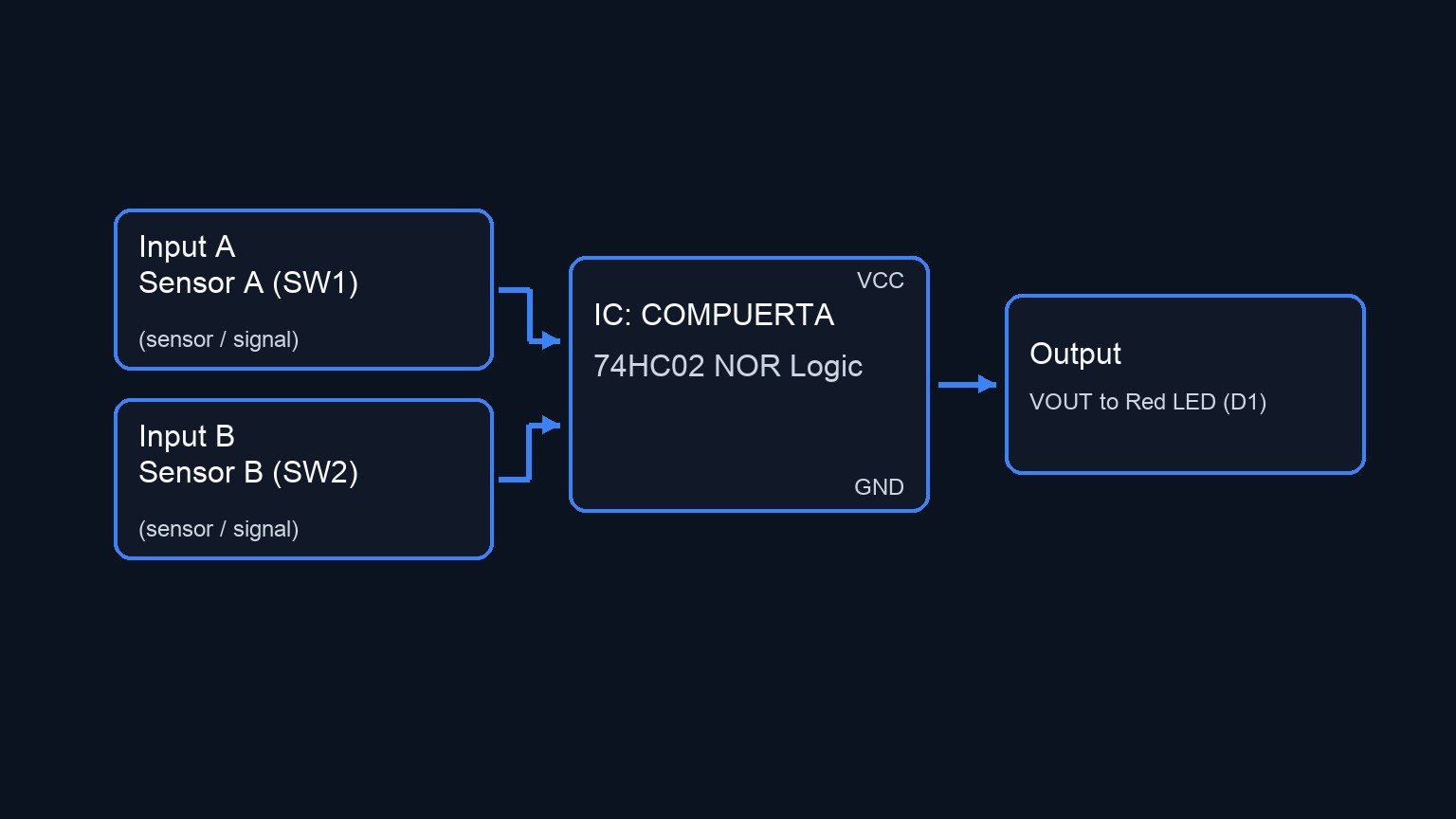
Follow me: