Level: Advanced. Implement a gated clock circuit allowing synchronization pulses only when Data Ready and System Enable are active.
Objective and use case
In this session, you will design and analyze a clock gating circuit using cascaded AND gates to control the flow of high-speed clock pulses to a shift register. You will validate that the clock signal only propagates when two distinct control flags (‘Data Ready’ and ‘System Enable’) are simultaneously high.
Why it is useful:
* Power Management: Disabling the clock tree to idle shift registers or sub-systems reduces dynamic power consumption in CMOS circuits.
* Data Integrity: Ensures data is only clocked into the buffer when the source indicates valid data (Data Ready) and the controller allows reception (System Enable).
* Bus Arbitration: Prevents bus contention by synchronizing multiple peripherals sharing a common data line.
Expected outcome:
* The output GATED_CLK mirrors the input CLK only when DATA_RDY = 1 and SYS_EN = 1.
* Propagation delay between input clock edge and output clock edge is measured (typically 7–15 ns for 74HC series).
* Identification of «runt pulses» or glitches if enable signals change state while the clock is high.
Target audience and level:
Electronics engineering students and embedded system designers (Advanced).
Materials
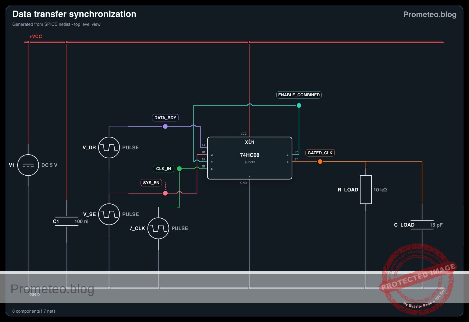
- U1: 74HC08 Quad 2-input AND gate IC, function: logic gating
- V_CLK: Pulse generator, function: Master Clock (1 MHz, 0V-5V)
- V_DR: DC voltage source or Switch, function: Data Ready signal
- V_SE: DC voltage source or Switch, function: System Enable signal
- V1: 5 V DC supply, function: Main power
- C1: 100 nF ceramic capacitor, function: U1 decoupling
- R_LOAD: 10 kΩ resistor, function: Simulates input impedance of shift register
- C_LOAD: 15 pF capacitor, function: Simulates input capacitance and probe load
Pin-out of the IC used
Selected Chip: 74HC08 (Quad 2-Input AND Gate)
| Pin | Name | Logic function | Connection in this case |
|---|---|---|---|
| 1 | 1A | Input Gate 1 | Connects to Node DATA_RDY |
| 2 | 1B | Input Gate 1 | Connects to Node SYS_EN |
| 3 | 1Y | Output Gate 1 | Connects to Node ENABLE_COMBINED (Internal) |
| 4 | 2A | Input Gate 2 | Connects to Node ENABLE_COMBINED |
| 5 | 2B | Input Gate 2 | Connects to Node CLK_IN |
| 6 | 2Y | Output Gate 2 | Connects to Node GATED_CLK |
| 7 | GND | Ground | Connects to Node 0 |
| 14 | VCC | Power Supply | Connects to Node VCC |
Wiring guide
Construct the circuit following these node connections. Ensure the power supply is off while wiring.
-
Power Supply:
- V1 positive terminal connects to node VCC.
- V1 negative terminal connects to node 0 (GND).
- C1 connects between VCC and 0 (placed close to U1).
- U1 Pin 14 connects to VCC.
- U1 Pin 7 connects to 0.
-
Control Logic (Gate 1):
- V_DR (Data Ready) positive terminal connects to node DATA_RDY.
- V_SE (System Enable) positive terminal connects to node SYS_EN.
- U1 Pin 1 (1A) connects to node DATA_RDY.
- U1 Pin 2 (1B) connects to node SYS_EN.
- U1 Pin 3 (1Y) connects to node ENABLE_COMBINED.
-
Clock Gating (Gate 2):
- V_CLK (Clock Source) positive terminal connects to node CLK_IN.
- U1 Pin 4 (2A) connects to node ENABLE_COMBINED.
- U1 Pin 5 (2B) connects to node CLK_IN.
- U1 Pin 6 (2Y) connects to node GATED_CLK.
-
Output Loading:
- R_LOAD connects between GATED_CLK and 0.
- C_LOAD connects between GATED_CLK and 0.
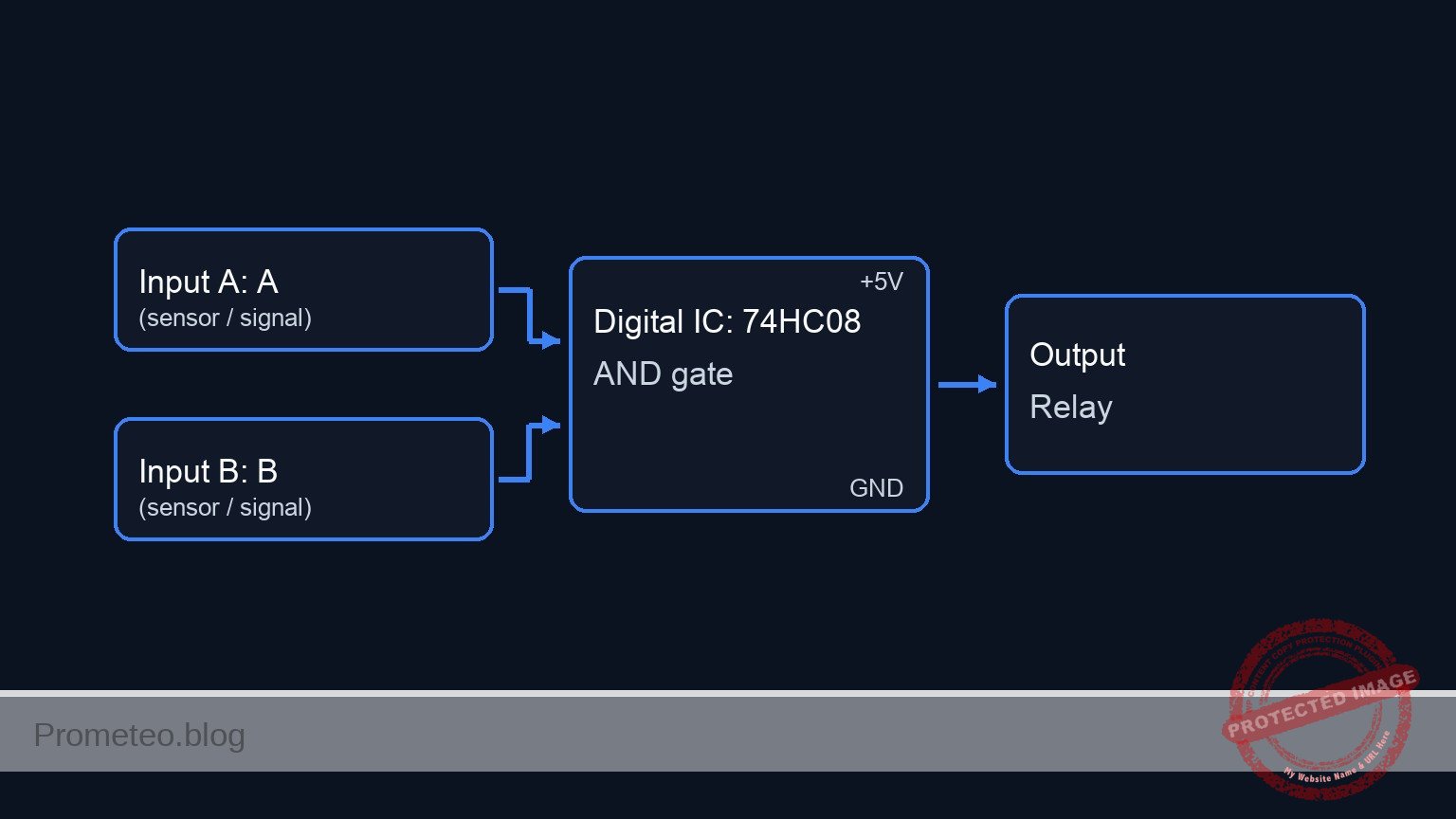
Conceptual block diagram
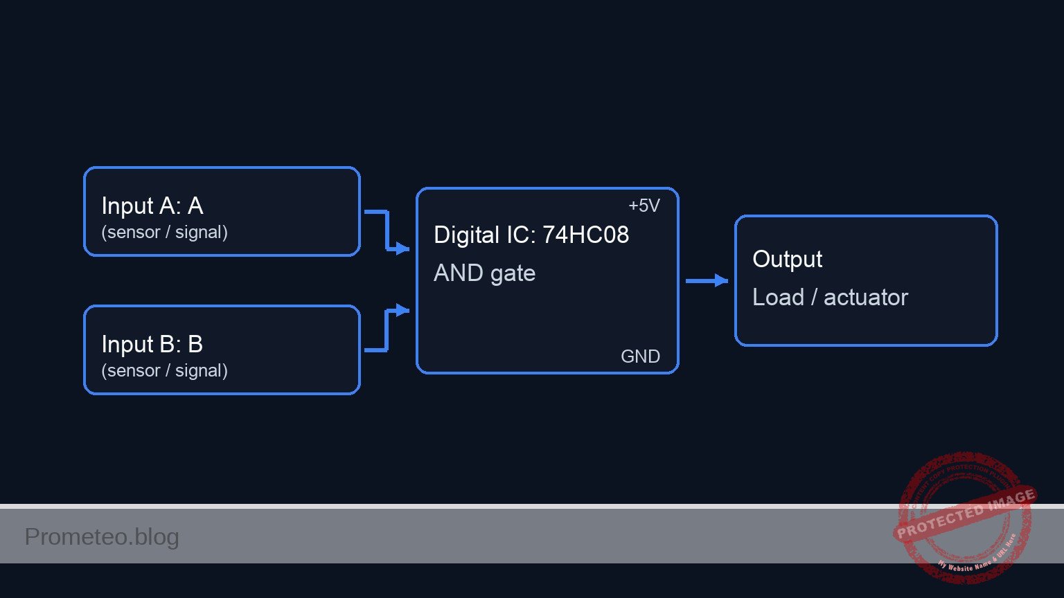
Schematic
[ INPUT SIGNALS ]                       [ LOGIC PROCESSING (U1: 74HC08) ]                     [ OUTPUT STAGE ]

                                             +-----------------------------------+
                                             |    POWER SUPPLY & DECOUPLING      |
                                             |  V1 (5V) -> Pin 14, GND -> Pin 7  |
                                             |  C1 (100nF) across VCC/GND        |
                                             +-----------------------------------+
                                                               |
    [ V_DR: Data Ready ] --(Pin 1)-->+                         |
                                     |                         v
                                     +-----> [ AND Gate 1 ] ---+
                                     |       (Control Logic)   |
    [ V_SE: Sys Enable ] --(Pin 2)-->+                         |
                                                               |
                                                               | (Pin 3: ENABLE_COMBINED)
                                                               |
                                                               v
                                                          (Pin 4)
                                                               +---> [ AND Gate 2 ] --(Pin 6)--> [ R_LOAD (10k) ] --+
                                                               |     (Clock Gating)              [ C_LOAD (15pF) ]  |
    [ V_CLK: Master Clk ] --(Pin 5)----------------------------+     (Signal: GATED_CLK)                            v
                                                                                                                   GND
Electrical diagram
Truth table
This table represents the cascaded logic: GATED_CLK = (DATA_RDY AND SYS_EN) AND CLK_IN.
| DATA_RDY | SYS_EN | ENABLE_COMBINED (Internal) | CLK_IN | GATED_CLK | State Description |
|---|---|---|---|---|---|
| 0 | X | 0 | X | 0 | Blocked: Data not ready |
| X | 0 | 0 | X | 0 | Blocked: System disabled |
| 1 | 1 | 1 | 0 | 0 | Active: Clock Low phase |
| 1 | 1 | 1 | 1 | 1 | Active: Clock High phase passed |
(X = Don’t Care)
Measurements and tests
Perform the following validation steps using an oscilloscope (Dual Channel recommended).
-
Static Logic Validation:
- Set V_CLK to 0V. Toggle V_DR and V_SE. Ensure GATED_CLK remains 0V.
- Set V_CLK to 5V (DC). Ensure GATED_CLK is High ONLY when both V_DR and V_SE are High.
-
Dynamic Clock Gating:
- Configure V_CLK to a 1 MHz square wave (50% duty cycle).
- Enable Channel 1 on CLK_IN and Channel 2 on GATED_CLK.
- Activate both V_DR and V_SE. Verify Channel 2 replicates Channel 1.
- Deactivate V_DR. Verify Channel 2 goes flat Low.
-
Propagation Delay Analysis (Advanced):
- With the clock running and passing through, maximize horizontal zoom (timebase ~10ns/div).
- Measure the time difference between the 50% voltage point of the rising edge of CLK_IN and the rising edge of GATED_CLK.
- Expected Result: A delay of approximately 15ns–25ns (sum of delays through Gate 1 and Gate 2).
-
Glitch/Hazard Observation:
- While CLK_IN is High, manually toggle DATA_RDY.
- Observe if truncated pulses («runts») appear on the output. These are hazards caused by asynchronous gating.
SPICE netlist and simulation
Reference SPICE Netlist (ngspice) — excerptFull SPICE netlist (ngspice)
* Practical case: Data transfer synchronization

* --- Power Supply ---
* V1 positive terminal connects to node VCC. Negative to node 0 (GND).
V1 VCC 0 DC 5
* C1 connects between VCC and 0 (placed close to U1).
C1 VCC 0 100n

* --- Input Stimuli (Dynamic) ---
* V_CLK: Master Clock (1 MHz, 0V-5V).
* PULSE(V1 V2 TD TR TF PW PER) -> 1us Period, 0.49us Width
V_CLK CLK_IN 0 PULSE(0 5 0 10n 10n 490n 1u)

* V_DR: Data Ready signal.
* Simulates a data packet ready signal. Pulses High from 5us to 15us.
V_DR DATA_RDY 0 PULSE(0 5 5u 10n 10n 10u 40u)

* V_SE: System Enable signal.
* Simulates system enable window. Pulses High from 2us to 22us.
V_SE SYS_EN 0 PULSE(0 5 2u 10n 10n 20u 50u)

* --- Control Logic (U1: 74HC08) ---
* Instantiation of the IC using a behavioral subcircuit.
* Mapping pins according to Wiring Guide:
* Pin 1 (1A) -> DATA_RDY
* Pin 2 (1B) -> SYS_EN
* Pin 3 (1Y) -> ENABLE_COMBINED
* Pin 4 (2A) -> ENABLE_COMBINED
* Pin 5 (2B) -> CLK_IN
* Pin 6 (2Y) -> GATED_CLK
* ... (truncated in public view) ...
Copy this content into a .cir file and run with ngspice.
* Practical case: Data transfer synchronization

* --- Power Supply ---
* V1 positive terminal connects to node VCC. Negative to node 0 (GND).
V1 VCC 0 DC 5
* C1 connects between VCC and 0 (placed close to U1).
C1 VCC 0 100n

* --- Input Stimuli (Dynamic) ---
* V_CLK: Master Clock (1 MHz, 0V-5V).
* PULSE(V1 V2 TD TR TF PW PER) -> 1us Period, 0.49us Width
V_CLK CLK_IN 0 PULSE(0 5 0 10n 10n 490n 1u)

* V_DR: Data Ready signal.
* Simulates a data packet ready signal. Pulses High from 5us to 15us.
V_DR DATA_RDY 0 PULSE(0 5 5u 10n 10n 10u 40u)

* V_SE: System Enable signal.
* Simulates system enable window. Pulses High from 2us to 22us.
V_SE SYS_EN 0 PULSE(0 5 2u 10n 10n 20u 50u)

* --- Control Logic (U1: 74HC08) ---
* Instantiation of the IC using a behavioral subcircuit.
* Mapping pins according to Wiring Guide:
* Pin 1 (1A) -> DATA_RDY
* Pin 2 (1B) -> SYS_EN
* Pin 3 (1Y) -> ENABLE_COMBINED
* Pin 4 (2A) -> ENABLE_COMBINED
* Pin 5 (2B) -> CLK_IN
* Pin 6 (2Y) -> GATED_CLK
* Pin 7 (GND)-> 0
* Pin 14(VCC)-> VCC
XU1 DATA_RDY SYS_EN ENABLE_COMBINED ENABLE_COMBINED CLK_IN GATED_CLK 0 VCC 74HC08_BEHAVIORAL

* --- Output Loading ---
* R_LOAD connects between GATED_CLK and 0.
R_LOAD GATED_CLK 0 10k
* C_LOAD connects between GATED_CLK and 0.
C_LOAD GATED_CLK 0 15p

* --- Subcircuit Model: 74HC08 ---
* Robust behavioral implementation using sigmoid functions for convergence.
* Only the gates used in the wiring are modeled to save complexity.
.subckt 74HC08_BEHAVIORAL 1A 1B 1Y 2A 2B 2Y GND VCC
    * Gate 1: 1Y = 1A AND 1B
    * Function: V(VCC) * Sigmoid(A) * Sigmoid(B)
    B_G1 1Y_INT GND V = V(VCC) * (1 / (1 + exp(-50*(V(1A)-2.5)))) * (1 / (1 + exp(-50*(V(1B)-2.5))))
    R_G1 1Y_INT 1Y 100

    * Gate 2: 2Y = 2A AND 2B
    B_G2 2Y_INT GND V = V(VCC) * (1 / (1 + exp(-50*(V(2A)-2.5)))) * (1 / (1 + exp(-50*(V(2B)-2.5))))
    R_G2 2Y_INT 2Y 100
.ends

* --- Analysis Directives ---
.op
* Transient analysis: 10ns step, 25us duration to capture full logic sequence
.tran 10n 25u

* --- Output Directives ---
.print tran V(CLK_IN) V(DATA_RDY) V(SYS_EN) V(ENABLE_COMBINED) V(GATED_CLK)

.end
Simulation Results (Transient Analysis)

Show raw data table (6072 rows)
Index   time            v(clk_in)       v(data_rdy)     v(sys_en)
0	0.000000e+00	0.000000e+00	0.000000e+00	0.000000e+00
1	1.000000e-10	5.000000e-02	0.000000e+00	0.000000e+00
2	2.000000e-10	1.000000e-01	0.000000e+00	0.000000e+00
3	4.000000e-10	2.000000e-01	0.000000e+00	0.000000e+00
4	8.000000e-10	4.000000e-01	0.000000e+00	0.000000e+00
5	1.600000e-09	8.000000e-01	0.000000e+00	0.000000e+00
6	3.200000e-09	1.600000e+00	0.000000e+00	0.000000e+00
7	6.400000e-09	3.200000e+00	0.000000e+00	0.000000e+00
8	1.000000e-08	5.000000e+00	0.000000e+00	0.000000e+00
9	1.064000e-08	5.000000e+00	0.000000e+00	0.000000e+00
10	1.192000e-08	5.000000e+00	0.000000e+00	0.000000e+00
11	1.448000e-08	5.000000e+00	0.000000e+00	0.000000e+00
12	1.960000e-08	5.000000e+00	0.000000e+00	0.000000e+00
13	2.960000e-08	5.000000e+00	0.000000e+00	0.000000e+00
14	3.960000e-08	5.000000e+00	0.000000e+00	0.000000e+00
15	4.960000e-08	5.000000e+00	0.000000e+00	0.000000e+00
16	5.960000e-08	5.000000e+00	0.000000e+00	0.000000e+00
17	6.960000e-08	5.000000e+00	0.000000e+00	0.000000e+00
18	7.960000e-08	5.000000e+00	0.000000e+00	0.000000e+00
19	8.960000e-08	5.000000e+00	0.000000e+00	0.000000e+00
20	9.960000e-08	5.000000e+00	0.000000e+00	0.000000e+00
21	1.096000e-07	5.000000e+00	0.000000e+00	0.000000e+00
22	1.196000e-07	5.000000e+00	0.000000e+00	0.000000e+00
23	1.296000e-07	5.000000e+00	0.000000e+00	0.000000e+00
... (6048 more rows) ...
Reference SPICE netlist (ngspice)
* Practical case: Data transfer synchronization

* --- Power Supply ---
* V1 positive terminal connects to node VCC. Negative to node 0 (GND).
V1 VCC 0 DC 5
* C1 connects between VCC and 0 (placed close to U1).
C1 VCC 0 100n

* --- Input Stimuli (Dynamic) ---
* V_CLK: Master Clock (1 MHz, 0V-5V).
* PULSE(V1 V2 TD TR TF PW PER) -> 1us Period, 0.49us Width
V_CLK CLK_IN 0 PULSE(0 5 0 10n 10n 490n 1u)

* V_DR: Data Ready signal.
* Simulates a data packet ready signal. Pulses High from 5us to 15us.
V_DR DATA_RDY 0 PULSE(0 5 5u 10n 10n 10u 40u)

* V_SE: System Enable signal.
* Simulates system enable window. Pulses High from 2us to 22us.
V_SE SYS_EN 0 PULSE(0 5 2u 10n 10n 20u 50u)

* --- Control Logic (U1: 74HC08) ---
* Instantiation of the IC using a behavioral subcircuit.
* Mapping pins according to Wiring Guide:
* Pin 1 (1A) -> DATA_RDY
* Pin 2 (1B) -> SYS_EN
* Pin 3 (1Y) -> ENABLE_COMBINED
* Pin 4 (2A) -> ENABLE_COMBINED
* Pin 5 (2B) -> CLK_IN
* Pin 6 (2Y) -> GATED_CLK
* Pin 7 (GND)-> 0
* Pin 14(VCC)-> VCC
XU1 DATA_RDY SYS_EN ENABLE_COMBINED ENABLE_COMBINED CLK_IN GATED_CLK 0 VCC 74HC08_BEHAVIORAL

* --- Output Loading ---
* R_LOAD connects between GATED_CLK and 0.
R_LOAD GATED_CLK 0 10k
* C_LOAD connects between GATED_CLK and 0.
C_LOAD GATED_CLK 0 15p

* --- Subcircuit Model: 74HC08 ---
* Robust behavioral implementation using sigmoid functions for convergence.
* Only the gates used in the wiring are modeled to save complexity.
.subckt 74HC08_BEHAVIORAL 1A 1B 1Y 2A 2B 2Y GND VCC
    * Gate 1: 1Y = 1A AND 1B
    * Function: V(VCC) * Sigmoid(A) * Sigmoid(B)
    B_G1 1Y_INT GND V = V(VCC) * (1 / (1 + exp(-50*(V(1A)-2.5)))) * (1 / (1 + exp(-50*(V(1B)-2.5))))
    R_G1 1Y_INT 1Y 100

    * Gate 2: 2Y = 2A AND 2B
    B_G2 2Y_INT GND V = V(VCC) * (1 / (1 + exp(-50*(V(2A)-2.5)))) * (1 / (1 + exp(-50*(V(2B)-2.5))))
    R_G2 2Y_INT 2Y 100
.ends

* --- Analysis Directives ---
.op
* Transient analysis: 10ns step, 25us duration to capture full logic sequence
.tran 10n 25u

* --- Output Directives ---
.print tran V(CLK_IN) V(DATA_RDY) V(SYS_EN) V(ENABLE_COMBINED) V(GATED_CLK)

.end
Simulation Results (Transient Analysis)
Common mistakes and how to avoid them
- Leaving unused inputs floating:
- Issue: Unused inputs on the 74HC08 (e.g., Pins 9, 10, 12, 13) pick up noise, causing high power consumption or oscillation.
- Solution: Connect all unused AND gate inputs directly to GND or VCC.
- Ignoring propagation delay accumulation:
- Issue: Assuming the output happens instantly. In this cascaded setup (Gate 1 -> Gate 2), the delay is double that of a single gate.
- Solution: Account for this delay in timing diagrams; signals may arrive too late for the setup time of the subsequent shift register.
- Gating the clock asynchronously:
- Issue: Changing SYS_EN while the clock is High clips the pulse width, violating the minimum pulse width requirement of the shift register.
- Solution: Ideally, synchronize the Enable signal to the falling edge of the clock (using a Flip-Flop) before feeding it to the AND gate.
Troubleshooting
- Symptom: Output is permanently Low, even when all inputs are High.
- Cause: Missing power to Pin 14 or GND to Pin 7.
- Fix: Check VCC/GND continuity with a multimeter.
- Symptom: «Ghosting» or noisy edges on the oscilloscope.
- Cause: Lack of decoupling capacitor or long ground leads on probes.
- Fix: Install C1 (100nF) extremely close to the IC; use the ground spring on the probe tip.
- Symptom: Signal edges are very rounded (slow rise time).
- Cause: Capacitive loading is too high (long wires or breadboard stray capacitance).
- Fix: Shorten wires or add a buffer if driving a heavy load.
Possible improvements and extensions
- Glitch-free Gating: Add a D-Flip-Flop (e.g., 74HC74) to synchronize the ENABLE_COMBINED signal so it only changes state when the Clock is Low.
- Wait-State Insertion: Expand the circuit to assert a «BUSY» signal back to the controller whenever the clock is successfully gated, confirming data transfer is active.
More Practical Cases on Prometeo.blog
Find this product and/or books on this topic on Amazon
As an Amazon Associate, I earn from qualifying purchases. If you buy through this link, you help keep this project running.
Quick Quiz

Telecommunications Electronics Engineer and Computer Engineer (official degrees in Spain).