Level: Basic – Build a logic circuit to activate a pump only when soil is dry and water is available.
Objective and use case
In this practical case, you will build a safety interlock circuit using a 74HC08 AND gate. The circuit simulates a smart irrigation controller that decides whether to turn on a water pump based on two environmental conditions.
Why this is useful:
* Equipment Protection: Prevents pumps from running «dry» (without water input), which often causes mechanical failure.
* Resource Conservation: Ensures water is only dispensed when the soil actually needs moisture.
* Industrial Logic: Demonstrates the fundamental «safety interlock» concept used in heavy machinery (e.g., machine runs ONLY if guard is closed AND operator presses button).
* Digital Logic Basics: Provides a clear physical representation of the Boolean AND function ($Y = A \cdot B$).
Expected outcome:
* The Output LED (Pump) turns ON only when Switch A (Soil Sensor) is HIGH AND Switch B (Tank Sensor) is HIGH.
* If the Tank is Empty (Switch B = LOW), the pump remains OFF even if the soil is dry.
* Logic 0: Voltage $\approx$ 0 V. Logic 1: Voltage $\approx$ 5 V.
Target audience: Electronic students and hobbyists at a basic level.
Materials
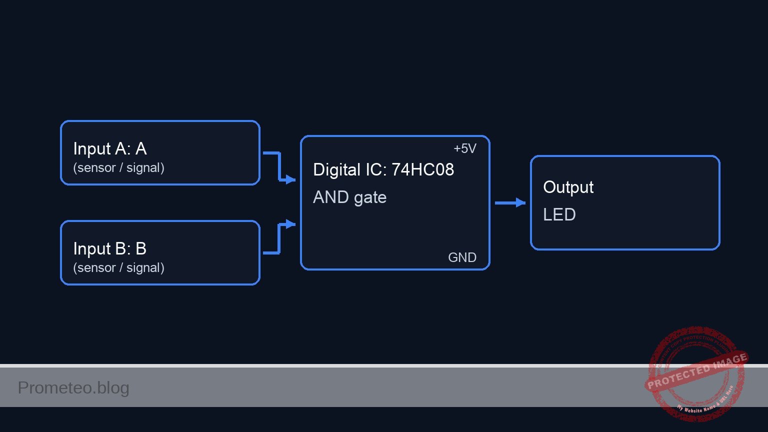
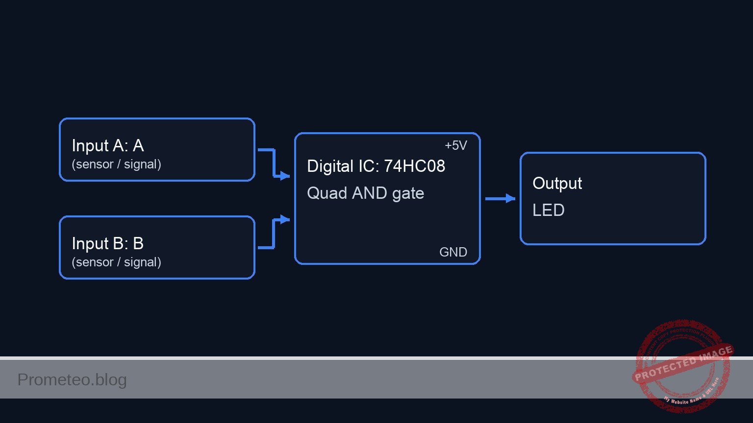
- U1: 74HC08, function: Quad 2-Input AND Gate IC.
- S1: SPST Switch, function: Soil Moisture Sensor simulation (Closed = Dry/Logic 1).
- S2: SPST Switch, function: Water Tank Level simulation (Closed = Water Present/Logic 1).
- R1: 10 kΩ resistor, function: pull-down for Input A.
- R2: 10 kΩ resistor, function: pull-down for Input B.
- R3: 330 Ω resistor, function: LED current limiting.
- D1: Green LED, function: Water Pump active indicator.
- V1: 5 V DC supply, function: Main power source.
Pin-out of the IC: 74HC08
The 74HC08 contains four independent AND gates. We will use only one of them for this experiment.
| Pin | Name | Logic Function | Connection in this case |
|---|---|---|---|
| 1 | 1A | Input A | Connected to S1 (Soil Status) |
| 2 | 1B | Input B | Connected to S2 (Tank Status) |
| 3 | 1Y | Output Y | Connected to LED (Pump indicator) |
| 7 | GND | Ground | Connected to Power Supply Ground (0V) |
| 14 | VCC | Power Supply | Connected to +5V Source |
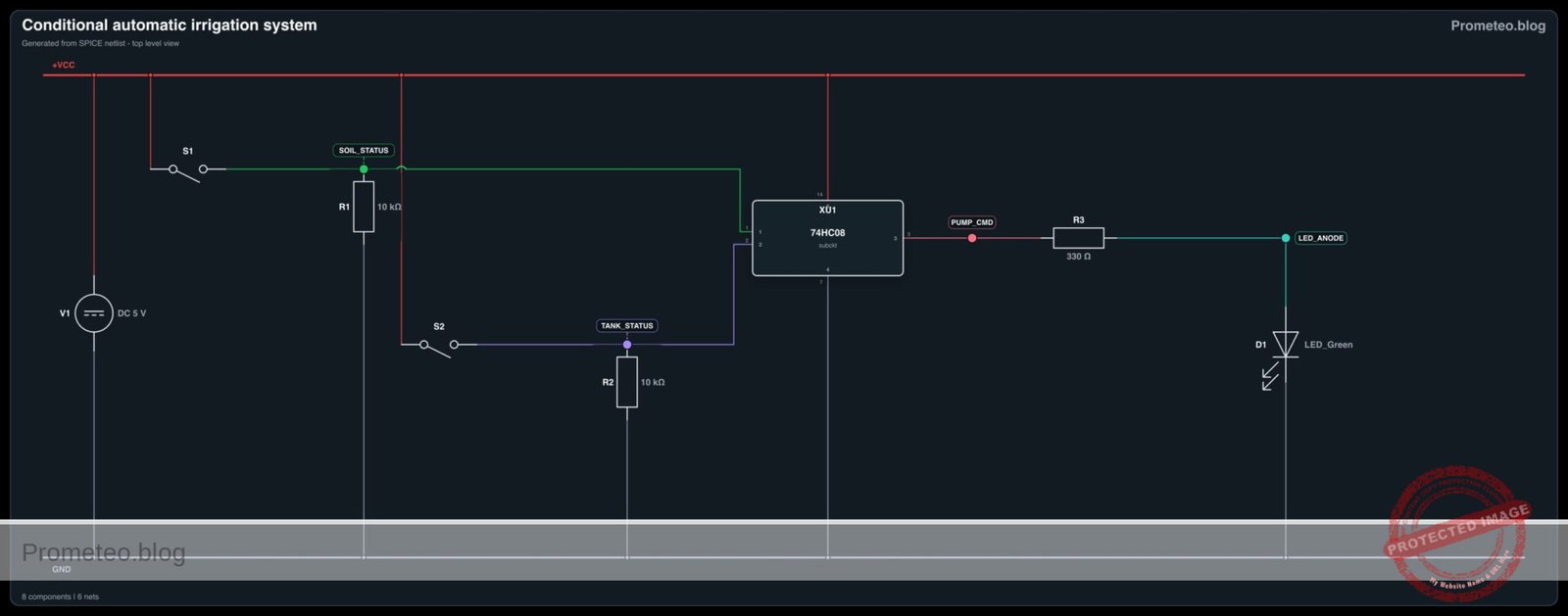
Wiring guide
Follow these connections carefully. The node names correspond to the function of the wire in the circuit.
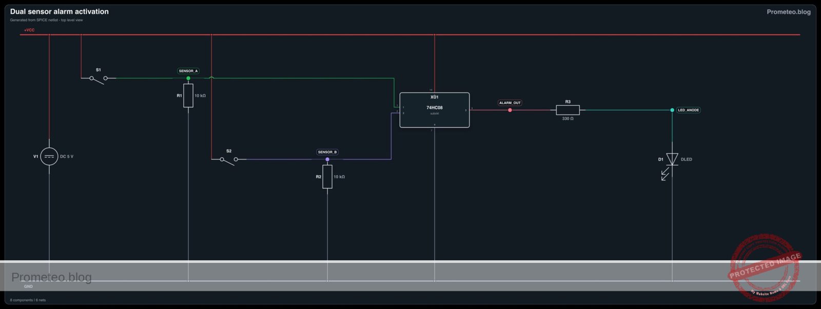
- V1 connects between node
VCCand node0(GND). - U1 (Pin 14) connects to node
VCC. - U1 (Pin 7) connects to node
0(GND). - S1 connects between node
VCCand nodeSOIL_Status. - R1 connects between node
SOIL_Statusand node0(GND) (Keeps input Low when switch is open). - S2 connects between node
VCCand nodeTANK_Status. - R2 connects between node
TANK_Statusand node0(GND) (Keeps input Low when switch is open). - U1 (Pin 1, Input A) connects to node
SOIL_Status. - U1 (Pin 2, Input B) connects to node
TANK_Status. - U1 (Pin 3, Output Y) connects to node
PUMP_Cmd. - R3 connects between node
PUMP_Cmdand nodeLED_Anode. - D1 connects between node
LED_Anode(Anode) and node0(GND) (Cathode).
Conceptual block diagram

Schematic
[ INPUTS ]                                  [ LOGIC ]                             [ OUTPUT ]

[ S1: Soil Sensor ]
[ (Switch to VCC) ] --(Node: SOIL_Status)-->+---------------------+
[ (R1: 10k to GND)]                         |      U1: 74HC08     |
                                            |      (AND Gate)     |
                                            |                     |--(Node: PUMP_Cmd)--> [ R3: 330 Ohm ] --> [ D1: Green LED ] --> GND
                                            |   Pin 1 (Input A)   |                      (Current Lim.)      (Pump Active)
                                            |                     |
                                            |   Pin 2 (Input B)   |
[ S2: Tank Level  ] --(Node: TANK_Status)-->|                     |
[ (Switch to VCC) ]                         +---------------------+
[ (R2: 10k to GND)]
Electrical diagram
Truth table
This table defines the logic states.
0 = Switch Open / 0V / Wet Soil / Empty Tank / Pump OFF
1 = Switch Closed / 5V / Dry Soil / Full Tank / Pump ON
| Soil Status (A) | Tank Status (B) | Output Pump (Y) | Real-world State |
|---|---|---|---|
| 0 | 0 | 0 | Soil wet, Tank empty -> Standby |
| 0 | 1 | 0 | Soil wet, Tank full -> Standby |
| 1 | 0 | 0 | Soil dry, Tank empty -> Safety Cutoff (Protect Pump) |
| 1 | 1 | 1 | Soil dry, Tank full -> Irrigation Active |
Measurements and tests
Validate your circuit using a multimeter set to DC Voltage (20V range).
- Standby Check: Ensure both S1 and S2 are Open (OFF). Measure voltage at Pin 3 of U1.
- Expected: ~0 V. D1 is OFF.
- Dry Run Protection Test: Close S1 (Soil is Dry) but leave S2 Open (Tank Empty).
- Expected: Pin 1 reads 5 V, Pin 2 reads 0 V. Output Pin 3 must remain at 0 V. D1 is OFF.
- No Demand Test: Open S1 (Soil Wet) and Close S2 (Tank Full).
- Expected: Pin 1 reads 0 V, Pin 2 reads 5 V. Output Pin 3 must remain at 0 V. D1 is OFF.
- Active Irrigation Test: Close both S1 and S2.
- Expected: Pin 1 reads 5 V, Pin 2 reads 5 V. Output Pin 3 should read ~5 V (Logic High). D1 lights up Green.
SPICE netlist and simulation
Reference SPICE Netlist (ngspice) — excerptFull SPICE netlist (ngspice)
* Title: Practical case: Conditional automatic irrigation system

* -----------------------------------------------------------------------------
* POWER SUPPLY
* -----------------------------------------------------------------------------
* V1: 5V DC supply, function: Main power source.
V1 VCC 0 DC 5

* -----------------------------------------------------------------------------
* STIMULI GENERATION (Simulating User Interaction)
* -----------------------------------------------------------------------------
* These voltage sources drive the control pins of the ideal switches (S1, S2)
* to simulate the physical sensors changing state over time.
* They are not part of the BOM but are necessary for dynamic simulation.

* Control signal for S1 (Soil Sensor): Period 200us
* Logic: 0 -> 1 -> 0 -> 1
V_CTRL_S1 N_CTRL_S1 0 PULSE(0 5 10u 1u 1u 100u 200u)

* Control signal for S2 (Tank Sensor): Period 400us
* Logic: 0 -> 0 -> 1 -> 1
V_CTRL_S2 N_CTRL_S2 0 PULSE(0 5 10u 1u 1u 200u 400u)

* -----------------------------------------------------------------------------
* INPUT STAGE (Sensors and Pull-downs)
* -----------------------------------------------------------------------------
* S1: SPST Switch, function: Soil Moisture Sensor simulation.
* Wiring: Connects between node VCC and node SOIL_Status.
* Logic: Closed (Controlled by V_CTRL_S1 High) = Dry/Logic 1.
S1 VCC SOIL_Status N_CTRL_S1 0 SW_IDEAL
* ... (truncated in public view) ...
Copy this content into a .cir file and run with ngspice.
* Title: Practical case: Conditional automatic irrigation system

* -----------------------------------------------------------------------------
* POWER SUPPLY
* -----------------------------------------------------------------------------
* V1: 5V DC supply, function: Main power source.
V1 VCC 0 DC 5

* -----------------------------------------------------------------------------
* STIMULI GENERATION (Simulating User Interaction)
* -----------------------------------------------------------------------------
* These voltage sources drive the control pins of the ideal switches (S1, S2)
* to simulate the physical sensors changing state over time.
* They are not part of the BOM but are necessary for dynamic simulation.

* Control signal for S1 (Soil Sensor): Period 200us
* Logic: 0 -> 1 -> 0 -> 1
V_CTRL_S1 N_CTRL_S1 0 PULSE(0 5 10u 1u 1u 100u 200u)

* Control signal for S2 (Tank Sensor): Period 400us
* Logic: 0 -> 0 -> 1 -> 1
V_CTRL_S2 N_CTRL_S2 0 PULSE(0 5 10u 1u 1u 200u 400u)

* -----------------------------------------------------------------------------
* INPUT STAGE (Sensors and Pull-downs)
* -----------------------------------------------------------------------------
* S1: SPST Switch, function: Soil Moisture Sensor simulation.
* Wiring: Connects between node VCC and node SOIL_Status.
* Logic: Closed (Controlled by V_CTRL_S1 High) = Dry/Logic 1.
S1 VCC SOIL_Status N_CTRL_S1 0 SW_IDEAL

* R1: 10 kΩ resistor, function: pull-down for Input A.
* Wiring: Connects between node SOIL_Status and node 0 (GND).
R1 SOIL_Status 0 10k

* S2: SPST Switch, function: Water Tank Level simulation.
* Wiring: Connects between node VCC and node TANK_Status.
* Logic: Closed (Controlled by V_CTRL_S2 High) = Water Present/Logic 1.
S2 VCC TANK_Status N_CTRL_S2 0 SW_IDEAL

* R2: 10 kΩ resistor, function: pull-down for Input B.
* Wiring: Connects between node TANK_Status and node 0 (GND).
R2 TANK_Status 0 10k

* -----------------------------------------------------------------------------
* LOGIC STAGE (74HC08 Quad 2-Input AND Gate)
* -----------------------------------------------------------------------------
* U1: 74HC08
* Wiring Guide:
* - Pin 1 (Input A) -> SOIL_Status
* - Pin 2 (Input B) -> TANK_Status
* - Pin 3 (Output Y) -> PUMP_Cmd
* - Pin 7 -> GND (0)
* - Pin 14 -> VCC
* Implemented as a subcircuit to strictly expose pins as nodes.
XU1 SOIL_Status TANK_Status PUMP_Cmd 0 VCC 74HC08_Behavioral

* -----------------------------------------------------------------------------
* OUTPUT STAGE (Indicator)
* -----------------------------------------------------------------------------
* R3: 330 Ω resistor, function: LED current limiting.
* Wiring: Connects between node PUMP_Cmd and node LED_Anode.
R3 PUMP_Cmd LED_Anode 330

* D1: Green LED, function: Water Pump active indicator.
* Wiring: Connects between node LED_Anode (Anode) and node 0 (GND).
D1 LED_Anode 0 LED_Green

* -----------------------------------------------------------------------------
* MODELS & SUBCIRCUITS
* -----------------------------------------------------------------------------
* Switch Model: Low On-Resistance, High Off-Resistance, Threshold 2.5V
.model SW_IDEAL SW(Vt=2.5 Ron=0.1 Roff=100Meg)

* LED Model: Generic Green LED approximation
.model LED_Green D(IS=1e-22 N=1.5 RS=5 BV=5 IBV=10u)

* 74HC08 Subcircuit (Behavioral Implementation)
* Pinout: 1=A, 2=B, 3=Y, 7=GND, 14=VCC
.subckt 74HC08_Behavioral 1 2 3 7 14
* Logic Y = A AND B
* Implementation: Continuous sigmoid function for robust convergence.
* Output voltage swings to V(14) (VCC) when both inputs > 2.5V.
B_AND 3 7 V = V(14,7) * (1 / (1 + exp(-40 * (V(1,7) - 2.5)))) * (1 / (1 + exp(-40 * (V(2,7) - 2.5))))
.ends

* -----------------------------------------------------------------------------
* ANALYSIS COMMANDS
* -----------------------------------------------------------------------------
* Transient analysis: 500us duration to capture all logic states (00, 10, 01, 11)
.tran 1u 500u

* Print critical nodes for verification
.print tran V(SOIL_Status) V(TANK_Status) V(PUMP_Cmd) V(LED_Anode)

* Calculate DC operating point
.op

.end
Simulation Results (Transient Analysis)

Show raw data table (1202 rows)
Index   time            v(soil_status)  v(tank_status)  v(pump_cmd)
0	0.000000e+00	4.999500e-04	4.999500e-04	7.201843e-87
1	1.000000e-08	4.999500e-04	4.999500e-04	7.201843e-87
2	2.000000e-08	4.999500e-04	4.999500e-04	7.201843e-87
3	4.000000e-08	4.999500e-04	4.999500e-04	7.201843e-87
4	8.000000e-08	4.999500e-04	4.999500e-04	7.201843e-87
5	1.600000e-07	4.999500e-04	4.999500e-04	7.201843e-87
6	3.200000e-07	4.999500e-04	4.999500e-04	7.201843e-87
7	6.400000e-07	4.999500e-04	4.999500e-04	7.201843e-87
8	1.280000e-06	4.999500e-04	4.999500e-04	7.201843e-87
9	2.280000e-06	4.999500e-04	4.999500e-04	7.201843e-87
10	3.280000e-06	4.999500e-04	4.999500e-04	7.201843e-87
11	4.280000e-06	4.999500e-04	4.999500e-04	7.201843e-87
12	5.280000e-06	4.999500e-04	4.999500e-04	7.201843e-87
13	6.280000e-06	4.999500e-04	4.999500e-04	7.201843e-87
14	7.280000e-06	4.999500e-04	4.999500e-04	7.201843e-87
15	8.280000e-06	4.999500e-04	4.999500e-04	7.201843e-87
16	9.280000e-06	4.999500e-04	4.999500e-04	7.201843e-87
17	1.000000e-05	4.999500e-04	4.999500e-04	7.201843e-87
18	1.010000e-05	4.999500e-04	4.999500e-04	7.201843e-87
19	1.026000e-05	4.999500e-04	4.999500e-04	7.201843e-87
20	1.030750e-05	4.999500e-04	4.999500e-04	7.201843e-87
21	1.039062e-05	4.999500e-04	4.999500e-04	7.201843e-87
22	1.041363e-05	4.999500e-04	4.999500e-04	7.201843e-87
23	1.045390e-05	4.999500e-04	4.999500e-04	7.201843e-87
... (1178 more rows) ...
Common mistakes and how to avoid them
- Floating Inputs: Forgetting R1 or R2 causes the inputs to «float,» making the LED flicker or turn on randomly when switches are open. Solution: Always verify pull-down resistors are connected to Ground.
- LED Orientation: Placing the LED backwards prevents it from lighting up even when logic is correct. Solution: Ensure the longer leg (Anode) faces the resistor and the IC.
- Confusing Chips: Using a 74HC32 (OR gate) instead of 74HC08 (AND gate). Solution: Read the text printed on the top of the IC before insertion. If it behaves like «Pump on if EITHER condition is met,» you have the wrong chip.
Troubleshooting
- Symptom: LED is always ON, regardless of switches.
- Cause: Inputs might be shorted directly to VCC, or the IC is damaged.
- Fix: Check wiring at Pin 1 and 2. Ensure R1 and R2 go to Ground, not VCC.
- Symptom: LED is very dim when active.
- Cause: R3 value is too high.
- Fix: Replace R3 with a value between 220 Ω and 470 Ω.
- Symptom: Circuit works inversely (LED off when switches are closed).
- Cause: You might be using a NAND gate (like 74HC00) or connected the LED to VCC instead of Ground (sourcing vs sinking).
- Fix: Verify part number is 74HC08 and LED Cathode is at Ground.
Possible improvements and extensions
- High Power Interface: Replace the LED with an NPN transistor (e.g., 2N2222) and a relay to control a real 12V water pump.
- Manual Override: Add a third switch connected to an OR gate after the AND gate output, allowing a user to force the pump ON regardless of sensors.
More Practical Cases on Prometeo.blog
Find this product and/or books on this topic on Amazon
As an Amazon Associate, I earn from qualifying purchases. If you buy through this link, you help keep this project running.
Quick Quiz

Telecommunications Electronics Engineer and Computer Engineer (official degrees in Spain).