Level: Medium | Use a capacitor to mitigate mechanical noise when actuating a physical switch.
Objective and use case
In this practical case, you will build a passive RC (Resistor-Capacitor) network connected to a mechanical switch to filter out the high-frequency voltage spikes generated by contact bounce.
Why this is useful:
* Preventing multiple false triggers in digital counters or step sequences.
* Ensuring clean, singular interrupt signals for microcontrollers.
* Stabilizing input readings for memory elements like flip-flops and latches.
* Creating reliable and predictable user-interface buttons in embedded systems.
Expected outcome:
* The mechanical bounce, normally lasting 1–5 ms, is completely absorbed by the capacitor.
* The voltage at the switch node transitions smoothly rather than oscillating between logic levels.
* The charging time constant defines a clean transient voltage curve upon button release.
* Oscilloscope measurements will confirm the elimination of the bounce time in milliseconds.
Target audience and level: Intermediate electronics students and hobbyists learning about transient signals and physical switch characteristics.
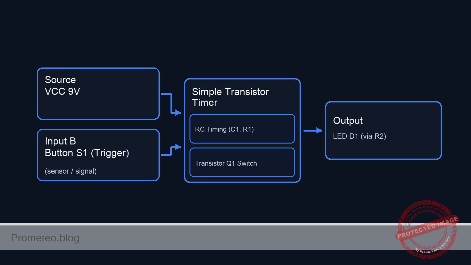
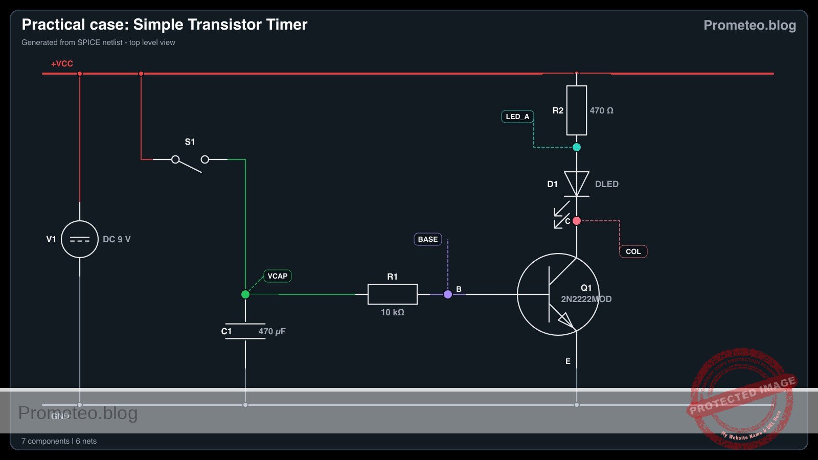
Materials
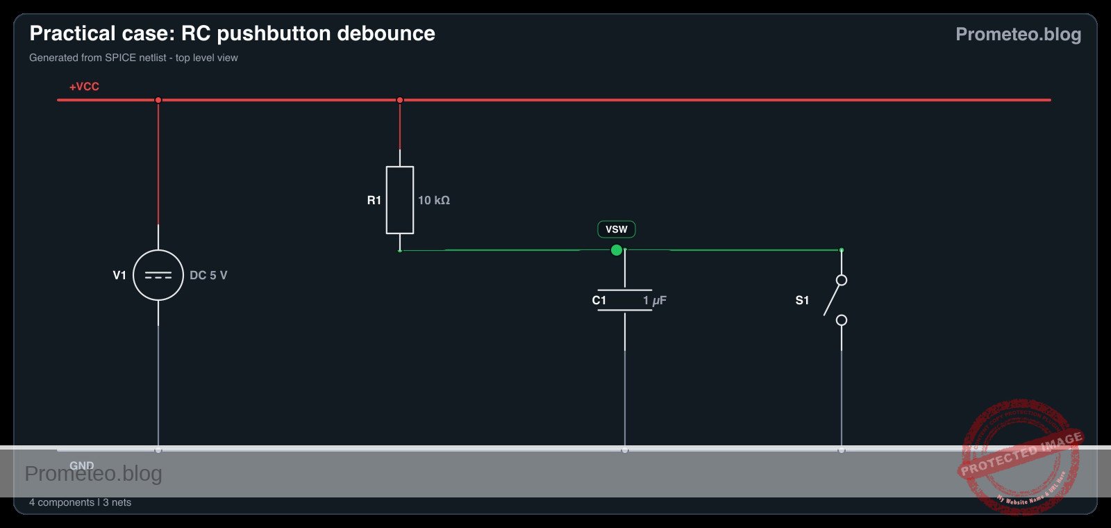
- V1: 5 V DC power supply
- SW1: SPST momentary pushbutton switch, function: input trigger
- R1: 10 kΩ resistor, function: pull-up for VSW
- C1: 1 µF capacitor, function: debounce smoothing parallel to switch
Wiring guide
- V1: connects between node VCC and node 0 (GND).
- R1: connects between node VCC and node VSW.
- SW1: connects between node VSW and node 0.
- C1: connects between node VSW and node 0.
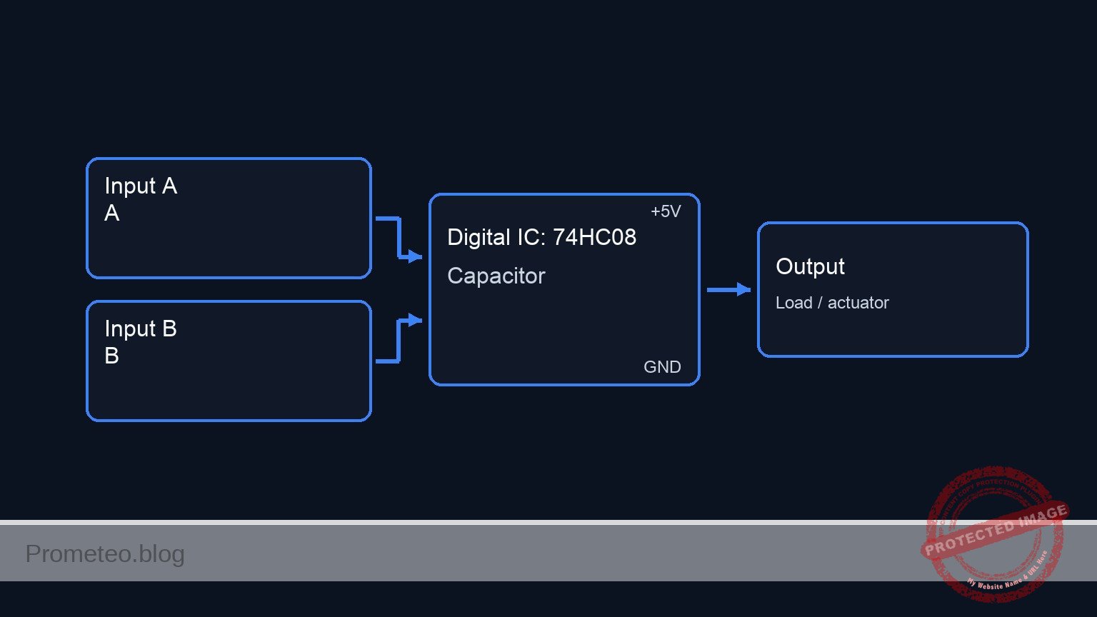
Conceptual block diagram
Schematic
VCC (5 V) --> [ R1: 10 kΩ Pull-up ] --+--(Node VSW)--> [ Debounced Output ]
                                    |
                                    +--> [ SW1: Pushbutton ] --> GND
                                    |
                                    +--> [ C1: 1µF Capacitor ] --> GND
Electrical diagram
Measurements and tests
- Connect an oscilloscope probe to node VSW and the ground clip to node 0.
- Set the oscilloscope to trigger on a falling edge at a threshold of approximately 2.5 V. Set the time base to 2 ms/div to accurately capture the Bounce-Time-ms.
- Actuate SW1 (press the button) and observe the Transient-Voltage on the screen. The voltage should drop to 0 V smoothly without the rapid spikes characteristic of mechanical bounce.
- Release the switch and observe the rising edge. Measure the time it takes for the voltage to reach 3.15 V (approx. 63.2% of 5 V). This represents one RC time constant (\tau = R × C), which should theoretically be 10 ms.
- Temporarily remove C1 from the circuit, press the switch again, and observe the raw mechanical bounce to compare the before-and-after transient signals. Reinsert C1 once complete.
SPICE netlist and simulation
Reference SPICE Netlist (ngspice) — excerptFull SPICE netlist (ngspice)
* Practical case: RC pushbutton debounce
.width out=256

* Main DC Power Supply
V1 VCC 0 DC 5

* Pull-up Resistor
R1 VCC VSW 10k

* Debounce Smoothing Capacitor
C1 VSW 0 1u

* Pushbutton SW1 modeled as a voltage-controlled switch
* Connects VSW to 0 (GND) when the control voltage is high
S1 VSW 0 ctrl 0 switch_model
.model switch_model SW(Vt=2.5 Ron=1 Roff=100Meg)

* Control pulse simulating the user pressing the button
* Presses the button at 5ms, holds for 20ms, repeats every 50ms
Vctrl ctrl 0 PULSE(0 5 5m 1u 1u 20m 50m)
* ... (truncated in public view) ...
Copy this content into a .cir file and run with ngspice.
* Practical case: RC pushbutton debounce
.width out=256

* Main DC Power Supply
V1 VCC 0 DC 5

* Pull-up Resistor
R1 VCC VSW 10k

* Debounce Smoothing Capacitor
C1 VSW 0 1u

* Pushbutton SW1 modeled as a voltage-controlled switch
* Connects VSW to 0 (GND) when the control voltage is high
S1 VSW 0 ctrl 0 switch_model
.model switch_model SW(Vt=2.5 Ron=1 Roff=100Meg)

* Control pulse simulating the user pressing the button
* Presses the button at 5ms, holds for 20ms, repeats every 50ms
Vctrl ctrl 0 PULSE(0 5 5m 1u 1u 20m 50m)

* Analysis directives
.op
.tran 100u 100m

* CRITICAL: Print input (button press) and output (debounced signal)
.print tran V(ctrl) V(VSW)

.end
Simulation Results (Transient Analysis)

Show raw data table (1134 rows)
Index   time            v(ctrl)         v(vsw)
0	0.000000e+00	0.000000e+00	4.999500e+00
1	1.000000e-06	0.000000e+00	4.999500e+00
2	2.000000e-06	0.000000e+00	4.999500e+00
3	4.000000e-06	0.000000e+00	4.999500e+00
4	8.000000e-06	0.000000e+00	4.999500e+00
5	1.600000e-05	0.000000e+00	4.999500e+00
6	3.200000e-05	0.000000e+00	4.999500e+00
7	6.400000e-05	0.000000e+00	4.999500e+00
8	1.280000e-04	0.000000e+00	4.999500e+00
9	2.280000e-04	0.000000e+00	4.999500e+00
10	3.280000e-04	0.000000e+00	4.999500e+00
11	4.280000e-04	0.000000e+00	4.999500e+00
12	5.280000e-04	0.000000e+00	4.999500e+00
13	6.280000e-04	0.000000e+00	4.999500e+00
14	7.280000e-04	0.000000e+00	4.999500e+00
15	8.280000e-04	0.000000e+00	4.999500e+00
16	9.280000e-04	0.000000e+00	4.999500e+00
17	1.028000e-03	0.000000e+00	4.999500e+00
18	1.128000e-03	0.000000e+00	4.999500e+00
19	1.228000e-03	0.000000e+00	4.999500e+00
20	1.328000e-03	0.000000e+00	4.999500e+00
21	1.428000e-03	0.000000e+00	4.999500e+00
22	1.528000e-03	0.000000e+00	4.999500e+00
23	1.628000e-03	0.000000e+00	4.999500e+00
... (1110 more rows) ...
Reference SPICE netlist (ngspice)
* Practical case: RC pushbutton debounce
.width out=256

* Main DC Power Supply
V1 VCC 0 DC 5

* Pull-up Resistor
R1 VCC VSW 10k

* Debounce Smoothing Capacitor
C1 VSW 0 1u

* Pushbutton SW1 modeled as a voltage-controlled switch
* Connects VSW to 0 (GND) when the control voltage is high
S1 VSW 0 ctrl 0 switch_model
.model switch_model SW(Vt=2.5 Ron=1 Roff=100Meg)

* Control pulse simulating the user pressing the button
* Presses the button at 5ms, holds for 20ms, repeats every 50ms
Vctrl ctrl 0 PULSE(0 5 5m 1u 1u 20m 50m)

* Analysis directives
.op
.tran 100u 100m

* CRITICAL: Print input (button press) and output (debounced signal)
.print tran V(ctrl) V(VSW)

.end
Simulation Results (Transient Analysis)
Common mistakes and how to avoid them
- Choosing a capacitor value that is too large: Using a 100 µF capacitor with a 10 kΩ pull-up results in a 1-second time constant, causing a sluggish button response. Solution: Keep C1 between 100 nF and 1 µF for standard 10 kΩ pull-up resistors.
- Missing the pull-up resistor: Without R1, node VSW will float unpredictably when the switch is open. Solution: Always ensure R1 is securely connected between VCC and the switch node.
- Feeding the slow RC signal directly into standard digital logic: Standard logic gates (like a basic 74HC08) can oscillate if fed a slowly rising voltage. Solution: Use this circuit to understand the RC transient, but for real digital inputs, feed the debounced signal through a Schmitt Trigger IC to square up the edges.
Troubleshooting
- Symptom: The voltage at node VSW remains constantly at 0 V.
- Cause: The switch is physically stuck closed, or the capacitor C1 is shorted.
- Fix: Check the switch continuity with a multimeter and replace C1 if defective.
- Symptom: The voltage at node VSW stays constantly at 5 V even when pressed.
- Cause: SW1 is not properly connected to node 0 (Ground).
- Fix: Verify the ground connection on the lower terminal of the switch.
- Symptom: Switch bounce is still visible on the rising edge.
- Cause: The RC time constant is too short compared to the mechanical bounce duration of that specific switch.
- Fix: Increase the value of C1 (e.g., from 0.1 µF to 1 µF).
- Symptom: The switch contacts fail or degrade after repeated presses.
- Cause: The capacitor dumps its charge instantly through the switch contacts, causing high inrush current.
- Fix: For long-term reliability, add a small 100 Ω resistor in series with the switch to limit the discharge current.
Possible improvements and extensions
- Add a Schmitt Trigger buffer: Route the VSW node through a Schmitt Trigger inverter (such as the 74HC14) to convert the exponential RC charging curve into a crisp, bounce-free digital logic pulse.
- Hardware vs Software Debounce comparison: Keep this hardware RC circuit on one button, and wire a raw button to a microcontroller. Implement a software debounce algorithm on the raw button and compare the resource usage and reliability of both methods.
More Practical Cases on Prometeo.blog
Find this product and/or books on this topic on Amazon
As an Amazon Associate, I earn from qualifying purchases. If you buy through this link, you help keep this project running.
Quick Quiz

Telecommunications Electronics Engineer and Computer Engineer (official degrees in Spain).