Practical case: Basic rectifier filtering

Basic rectifier filtering prototype (Maker Style)

Level: Basic. Demonstrate how a capacitor smoothes ripple in a half-wave rectified signal.

Objective and use case

In this practical case, you will build a half-wave rectifier circuit and observe the effect of adding a filter capacitor in parallel with the load.
* Why it is useful:
* Essential for converting Alternating Current (AC) from the mains into Direct Current (DC) for powering electronics.
* Used in simple battery chargers.
* Fundamental concept for audio signal demodulation (envelope detectors).
* Demonstrates energy storage properties of capacitors in power supplies.
* Expected outcome:
* Input: A pure AC sine wave (swinging positive and negative).
* Step 1 Output: A pulsing positive-only signal (half-wave rectification).
* Step 2 Output: A steady DC voltage with slight variation (ripple) after connecting the capacitor.
* Target audience and level: Students and hobbyists understanding basic AC/DC conversion.
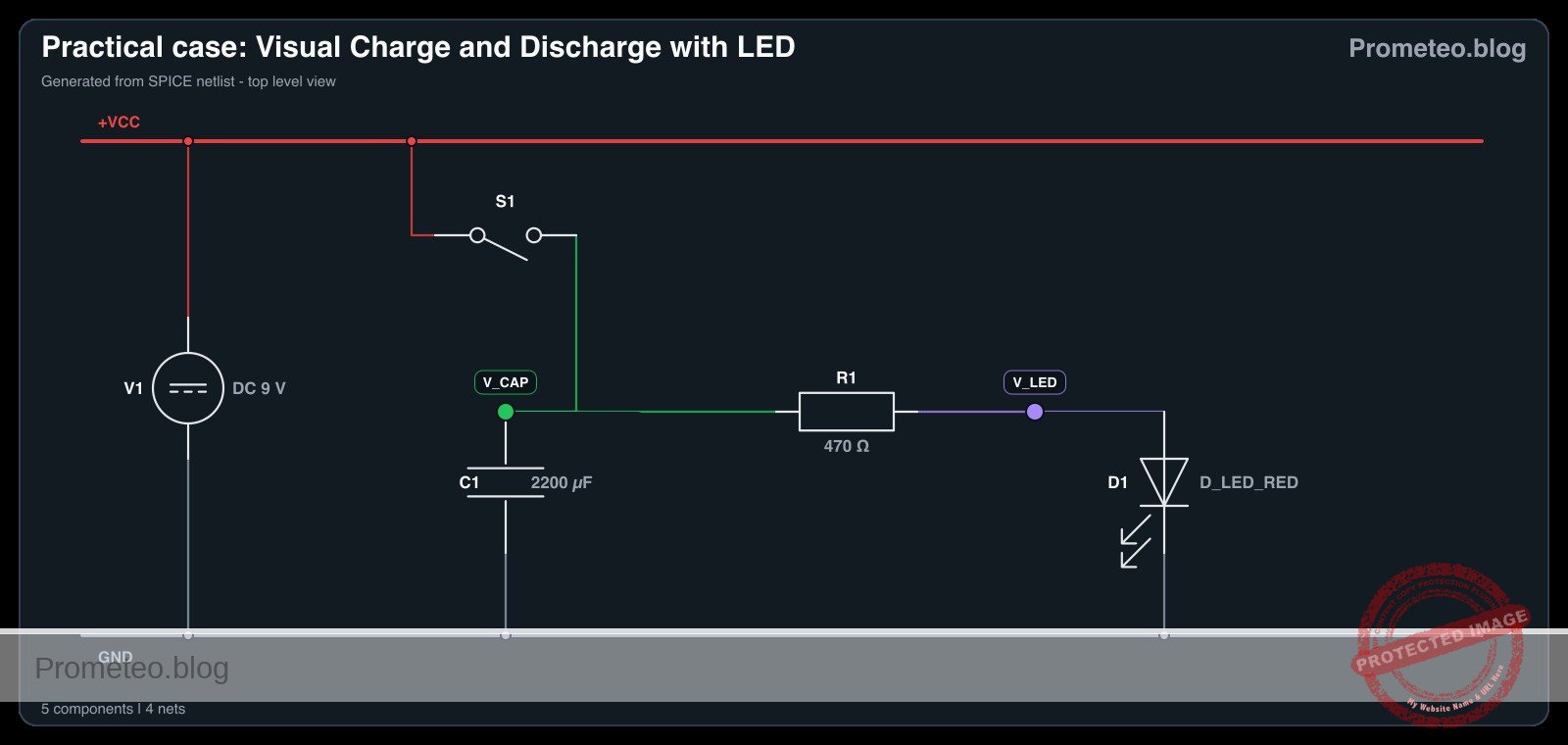
Materials

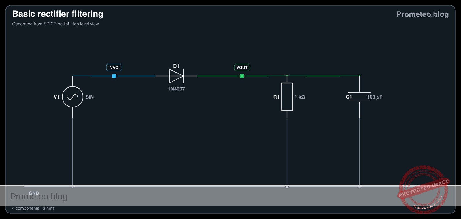
  • V1: 10 V (peak), 50 Hz sine wave source, function: AC power input.
  • D1: 1N4007 diode, function: rectifies AC to pulsating DC.
  • R1: 1 kΩ resistor, function: acts as the electrical load.
  • C1: 100 µF electrolytic capacitor, function: filters voltage ripple (stores energy).
  • GND: Ground reference (0 V).

Wiring guide

Construct the circuit following these node connections:

  • V1 (Source): Connect the positive terminal to node VAC and the negative terminal to node 0 (GND).
  • D1 (Rectifier): Connect the Anode to node VAC and the Cathode to node VOUT.
  • R1 (Load): Connect between node VOUT and node 0 (GND).
  • C1 (Filter): Connect the positive terminal to node VOUT and the negative terminal to node 0 (GND). Note: Initially leave C1 disconnected to observe the unfiltered signal, then connect it.

Conceptual block diagram

Conceptual block diagram — LM7805 Half-Wave Rectifier w/ Filter
Quick read: inputs → main block → output (actuator or measurement). This summarizes the ASCII schematic below.

Schematic

[ AC SOURCE ]            [ RECTIFICATION ]             [ OUTPUT STAGE ]

                                                          +--> [ C1 Filter ] --> GND
                                                          |    (100 uF)
    [ V1 Source ] --(VAC)--> [ D1 Diode ] --(VOUT Node)-->+
    (10 V, 50Hz)              (1N4007)                     |
                                                          +--> [ R1 Load ]   --> GND
                                                               (1 kOhm)
Schematic (ASCII)

Electrical diagram

Electrical diagram for case: Basic rectifier filtering
Generated from the validated SPICE netlist for this case.

🔒 This electrical diagram is premium. With the 7-day pass or the monthly membership you can unlock the complete didactic material and the print-ready PDF pack.🔓 See premium access plans

Measurements and tests

Perform the following steps using an oscilloscope or a multimeter:

  1. Input Verification:
    • Connect the probe to VAC.
    • Verify a sine wave oscillating between +10 V and -10 V.
  2. Unfiltered Rectification (C1 Disconnected):
    • Remove C1 temporarily.
    • Measure VOUT. You should see only the positive half-cycles of the sine wave (approx. 0 V to 9.3 V due to diode drop). The voltage drops to zero between peaks.
  3. Filtered Rectification (C1 Connected):
    • Connect C1 across R1.
    • Measure VOUT. The signal should now be a DC voltage near the peak value (approx. 9 V) that does not drop to zero.
    • Vripple Measurement: Set the oscilloscope to AC coupling to zoom in on the small voltage fluctuation («sawtooth» shape) on top of the DC line.

SPICE netlist and simulation

Reference SPICE Netlist (ngspice) — excerptFull SPICE netlist (ngspice)

* Basic rectifier filtering

* --- Components ---

* V1: 10 V (peak), 50 Hz sine wave source
* Connected: Positive -> VAC, Negative -> 0 (GND)
V1 VAC 0 SIN(0 10 50)

* D1: 1N4007 diode (Rectifier)
* Connected: Anode -> VAC, Cathode -> VOUT
D1 VAC VOUT 1N4007

* R1: 1 kΩ resistor (Load)
* Connected: Between VOUT and 0 (GND)
R1 VOUT 0 1k

* C1: 100 µF electrolytic capacitor (Filter)
* Connected: Positive -> VOUT, Negative -> 0 (GND)
* Note: Included to demonstrate the filtering effect described in the case.
C1 VOUT 0 100u
* ... (truncated in public view) ...

Copy this content into a .cir file and run with ngspice.

🔒 Part of this section is premium. With the 7-day pass or the monthly membership you can access the full content (materials, wiring, detailed build, validation, troubleshooting, variants and checklist) and download the complete print-ready PDF pack.

* Basic rectifier filtering

* --- Components ---

* V1: 10 V (peak), 50 Hz sine wave source
* Connected: Positive -> VAC, Negative -> 0 (GND)
V1 VAC 0 SIN(0 10 50)

* D1: 1N4007 diode (Rectifier)
* Connected: Anode -> VAC, Cathode -> VOUT
D1 VAC VOUT 1N4007

* R1: 1 kΩ resistor (Load)
* Connected: Between VOUT and 0 (GND)
R1 VOUT 0 1k

* C1: 100 µF electrolytic capacitor (Filter)
* Connected: Positive -> VOUT, Negative -> 0 (GND)
* Note: Included to demonstrate the filtering effect described in the case.
C1 VOUT 0 100u

* --- Models ---

* Standard silicon rectifier diode model approximation for 1N4007
.model 1N4007 D(IS=7.03n RS=0.04 N=1.85 CJO=10p VJ=1 M=0.5 BV=1000 IBV=10u TT=5u)

* --- Analysis Directives ---

* Transient analysis: 100ms duration (5 cycles of 50Hz) with 0.1ms step
.tran 0.1ms 100ms

* Operating point analysis
.op

* Print directives for simulation logging
.print tran V(VAC) V(VOUT)

.end

Simulation Results (Transient Analysis)

Simulation Results (Transient Analysis)
Show raw data table (1017 rows)
Index   time            v(vac)          v(vout)
0	0.000000e+00	0.000000e+00	-2.77024e-22
1	1.000000e-06	3.141593e-03	3.430255e-10
2	2.000000e-06	6.283185e-03	6.932562e-10
3	4.000000e-06	1.256637e-02	1.411758e-09
4	8.000000e-06	2.513271e-02	2.956960e-09
5	1.600000e-05	5.026527e-02	6.646271e-09
6	3.200000e-05	1.005293e-01	1.882015e-08
7	5.304087e-05	1.666251e-01	6.310202e-08
8	7.565486e-05	2.376544e-01	2.484107e-07
9	1.009625e-04	3.171298e-01	1.270798e-06
10	1.280850e-04	4.022822e-01	7.576310e-06
11	1.570209e-04	4.930958e-01	5.140208e-05
12	1.876236e-04	5.890955e-01	3.869871e-04
13	2.197798e-04	6.899101e-01	3.065854e-03
14	2.535671e-04	7.957622e-01	2.015809e-02
15	2.900907e-04	9.100857e-01	7.787813e-02
16	3.269176e-04	1.025237e+00	1.740794e-01
17	3.659101e-04	1.147010e+00	2.922342e-01
18	4.156771e-04	1.302180e+00	4.470469e-01
19	4.731074e-04	1.480844e+00	6.257990e-01
20	5.731074e-04	1.790758e+00	9.360689e-01
21	6.731074e-04	2.098905e+00	1.244455e+00
22	7.731074e-04	2.404980e+00	1.550935e+00
23	8.731074e-04	2.708681e+00	1.855020e+00
... (993 more rows) ...

Common mistakes and how to avoid them

  1. Reversing Capacitor Polarity:
    • Error: Connecting the negative leg of an electrolytic capacitor to the positive voltage node.
    • Solution: Always ensure the stripe (negative side) of the capacitor connects to Ground (0). Reverse polarity can cause the capacitor to explode.
  2. Load Resistance Too Low:
    • Error: Using a very small resistor (e.g., 10 Ω) with a small capacitor.
    • Solution: If the load draws too much current, the capacitor discharges too quickly, causing massive ripple. Increase C1 or R1.
  3. Ignoring Diode Voltage Drop:
    • Error: Expecting exactly 10 V DC from a 10 V AC peak source.
    • Solution: Account for the ~0.7 V drop across the silicon diode. Expect around 9.3 V peak.

Troubleshooting

  • Symptom: Output is identical to Input (AC sine wave).
    • Cause: Diode is shorted internally.
    • Fix: Replace D1.
  • Symptom: Output is 0 V.
    • Cause: Diode is open or connected backward (blocking positive cycle).
    • Fix: Check diode orientation (anode to source).
  • Symptom: Ripple is very high (voltage drops deeply between peaks).
    • Cause: Capacitor value is too low for the frequency or load.
    • Fix: Increase C1 to 470 µF or 1000 µF.

Possible improvements and extensions

  1. Full-Wave Rectification: Replace the single diode with a bridge rectifier (4 diodes) to utilize the negative half-cycle, doubling the ripple frequency and improving efficiency.
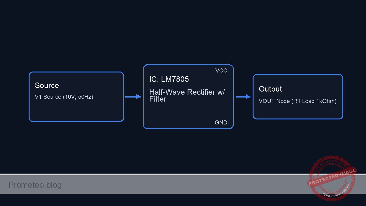
  2. Voltage Regulator: Add a Zener diode or a linear regulator (like an LM7805) after the capacitor to create a fixed, stable DC output regardless of ripple.

More Practical Cases on Prometeo.blog

Find this product and/or books on this topic on Amazon

Go to Amazon

As an Amazon Associate, I earn from qualifying purchases. If you buy through this link, you help keep this project running.

Quick Quiz

Question 1: What is the primary function of the 1N4007 diode (D1) in this circuit?


Question 2: What is the role of the capacitor C1 in the circuit?


Question 3: Before adding the capacitor, what does the output signal look like after passing through the diode?


Question 4: Which component acts as the electrical load in this specific circuit?


Question 5: What is the expected output after connecting the capacitor to the circuit?


Question 6: To which node should the Anode of the diode D1 be connected in a standard half-wave rectifier configuration?


Question 7: What is the frequency of the AC sine wave source (V1) specified for this experiment?


Question 8: Why is this circuit useful for powering electronics?


Question 9: Where should the negative terminal of the capacitor C1 be connected?


Question 10: Besides power supplies, what is another application mentioned for this fundamental concept?


Carlos Núñez Zorrilla
Electronics & Computer Engineer

Telecommunications Electronics Engineer and Computer Engineer (official degrees in Spain).

Follow me:


Practical case: Visual Charge and Discharge with LED

Visual Charge and Discharge with LED prototype (Maker Style)

Level: Basic – Observe energy storage in an electrolytic capacitor via LED fading.

Objective and use case

You will build a simple circuit where a capacitor acts as a temporary energy reservoir, keeping an LED illuminated briefly after the power source is disconnected.

  • Why it is useful:

    • Demonstrates how capacitors store and release electrical energy.
    • Simulates the «smoothing» effect used in power supply adapters to maintain steady voltage.
    • Visualizes the RC time constant (the relationship between resistance, capacitance, and time).
    • Introduces the concept of «hold-up time» in power failures.
  • Expected outcome:

    • Switch ON: The LED lights up immediately.
    • Switch OFF: The LED does not turn off instantly; instead, it slowly fades out over several seconds.
    • Visual: A smooth transition from bright light to darkness.
    • Audience: Students and hobbyists interested in basic component behavior.

Materials

  • V1: 9 V DC battery or power supply, function: main energy source.
  • S1: SPST toggle switch or push-button, function: controls the connection to the power source.
  • C1: 2200 µF electrolytic capacitor (16 V or higher), function: energy storage reservoir.
  • R1: 470 Ω resistor, function: LED current limiting and discharge timing control.
  • D1: Red LED, function: visual indicator of current flow and stored charge.

Wiring guide

Use the following explicit node connections to build the circuit. The standard ground reference is node 0.

  • Power and Switch:

    • Connect the Positive terminal of V1 to node VCC.
    • Connect the Negative terminal of V1 to node 0 (GND).
    • Connect one side of switch S1 to node VCC.
    • Connect the other side of switch S1 to node V_CAP.
  • Capacitor (The Tank):

    • Connect the Positive (long leg) of C1 to node V_CAP.
    • Connect the Negative (short leg/stripe) of C1 to node 0.
  • LED and Resistor (The Load):

    • Connect resistor R1 between node V_CAP and node V_LED.
    • Connect the Anode (long leg) of D1 to node V_LED.
    • Connect the Cathode (short leg/flat spot) of D1 to node 0.

Conceptual block diagram

Conceptual block diagram — RC Charge/Discharge Circuit
Quick read: inputs → main block → output (actuator or measurement). This summarizes the ASCII schematic below.

Schematic

Title: Practical case: Visual Charge and Discharge with LED

      [ INPUT / CONTROL ]               [ STORAGE / BUFFER ]               [ OUTPUT / LOAD ]

                                            (Node V_CAP)
    [ 9 V Battery ] --(+)--> [ Switch S1 ] -------+-------> [ Resistor R1 ] --> [ LED D1 ] --> GND
                                                 |
                                                 |
                                                 v
                                          [ Capacitor C1 ]
                                          (   2200 uF    )
                                                 |
                                                GND
Schematic (ASCII)

Electrical diagram

Electrical diagram for case: Visual Charge and Discharge with LED
Generated from the validated SPICE netlist for this case.

🔒 This electrical diagram is premium. With the 7-day pass or the monthly membership you can unlock the complete didactic material and the print-ready PDF pack.🔓 See premium access plans

Measurements and tests

  1. Initial State: Ensure S1 is Open (Off). The LED should be dark.
  2. Charge Phase: Close S1. Observe that the LED lights up instantly. The capacitor C1 charges to approximately 9 V almost immediately.
  3. Discharge Phase: Open S1.
    • Observe that the LED remains lit but begins to dim.
    • Use a stopwatch to measure the time from opening the switch until the LED is completely dark.
  4. Repeat: Swap C1 for a smaller value (e.g., 100 µF) and observe how the fade time becomes much shorter (almost instant).

SPICE netlist and simulation

Reference SPICE Netlist (ngspice) — excerptFull SPICE netlist (ngspice)

* Practical case: Visual Charge and Discharge with LED

* --- Power Supply (V1) ---
* 9V DC Battery connected to VCC and GND (0)
V1 VCC 0 DC 9

* --- Switch (S1) ---
* Modeled as a Voltage-Controlled Switch to simulate a physical push-button.
* Connections: VCC to V_CAP
* The switch is controlled by the voltage at node 'CTRL'.
S1 VCC V_CAP CTRL 0 SW_PUSH

* Switch Control Source (Simulates User Interaction)
* Simulates pressing the button at T=0.1s, holding for 1s, then releasing.
* PULSE(V1 V2 TD TR TF PW PER)
V_USER_S1 CTRL 0 PULSE(0 5 0.1 1m 1m 1 5)

* Switch Model Definition
* Ron=1 ohm represents wiring/contact resistance.
.model SW_PUSH SW(Vt=2.5 Ron=1 Roff=100Meg)
* ... (truncated in public view) ...

Copy this content into a .cir file and run with ngspice.

🔒 Part of this section is premium. With the 7-day pass or the monthly membership you can access the full content (materials, wiring, detailed build, validation, troubleshooting, variants and checklist) and download the complete print-ready PDF pack.

* Practical case: Visual Charge and Discharge with LED

* --- Power Supply (V1) ---
* 9V DC Battery connected to VCC and GND (0)
V1 VCC 0 DC 9

* --- Switch (S1) ---
* Modeled as a Voltage-Controlled Switch to simulate a physical push-button.
* Connections: VCC to V_CAP
* The switch is controlled by the voltage at node 'CTRL'.
S1 VCC V_CAP CTRL 0 SW_PUSH

* Switch Control Source (Simulates User Interaction)
* Simulates pressing the button at T=0.1s, holding for 1s, then releasing.
* PULSE(V1 V2 TD TR TF PW PER)
V_USER_S1 CTRL 0 PULSE(0 5 0.1 1m 1m 1 5)

* Switch Model Definition
* Ron=1 ohm represents wiring/contact resistance.
.model SW_PUSH SW(Vt=2.5 Ron=1 Roff=100Meg)

* --- Capacitor (C1) ---
* 2200uF Energy Storage
* Connections: V_CAP to GND (0)
C1 V_CAP 0 2200u

* --- Resistor (R1) ---
* 470 Ohm Current Limiting Resistor
* Connections: V_CAP to V_LED
R1 V_CAP V_LED 470

* --- LED (D1) ---
* Red LED Indicator
* Connections: Anode (V_LED) to Cathode (0)
D1 V_LED 0 D_LED_RED

* LED Model Definition
* Generic Red LED parameters
.model D_LED_RED D(IS=1e-14 N=2 RS=10 BV=5 IBV=10u)

* --- Analysis Commands ---
* The discharge time constant (Tau) = R * C = 470 * 2200e-6 approx 1.03 seconds.
* Simulation runs for 3 seconds to visualize the charge and discharge cycle.
.tran 10m 3s

* --- Output Directives ---
* Prints the capacitor voltage, LED anode voltage, and switch control signal.
.print tran V(V_CAP) V(V_LED) V(CTRL)

.op
.end

Simulation Results (Transient Analysis)

Simulation Results (Transient Analysis)
Show raw data table (352 rows)
Index   time            v(v_cap)        v(v_led)        v(ctrl)
0	0.000000e+00	8.234122e-01	8.233738e-01	0.000000e+00
1	1.000000e-04	8.234122e-01	8.233738e-01	0.000000e+00
2	2.000000e-04	8.234122e-01	8.233738e-01	0.000000e+00
3	4.000000e-04	8.234122e-01	8.233738e-01	0.000000e+00
4	8.000000e-04	8.234122e-01	8.233738e-01	0.000000e+00
5	1.600000e-03	8.234122e-01	8.233738e-01	0.000000e+00
6	3.200000e-03	8.234122e-01	8.233738e-01	0.000000e+00
7	6.400000e-03	8.234122e-01	8.233738e-01	0.000000e+00
8	1.280000e-02	8.234122e-01	8.233738e-01	0.000000e+00
9	2.280000e-02	8.234122e-01	8.233738e-01	0.000000e+00
10	3.280000e-02	8.234122e-01	8.233738e-01	0.000000e+00
11	4.280000e-02	8.234122e-01	8.233738e-01	0.000000e+00
12	5.280000e-02	8.234122e-01	8.233738e-01	0.000000e+00
13	6.280000e-02	8.234122e-01	8.233738e-01	0.000000e+00
14	7.280000e-02	8.234122e-01	8.233738e-01	0.000000e+00
15	8.280000e-02	8.234122e-01	8.233738e-01	0.000000e+00
16	9.280000e-02	8.234122e-01	8.233738e-01	0.000000e+00
17	1.000000e-01	8.234122e-01	8.233738e-01	0.000000e+00
18	1.001000e-01	8.234122e-01	8.233738e-01	5.000000e-01
19	1.002600e-01	8.234122e-01	8.233738e-01	1.300000e+00
20	1.003075e-01	8.234122e-01	8.233738e-01	1.537500e+00
21	1.003906e-01	8.234122e-01	8.233738e-01	1.953125e+00
22	1.004136e-01	8.234122e-01	8.233738e-01	2.068164e+00
23	1.004539e-01	8.234122e-01	8.233738e-01	2.269482e+00
... (328 more rows) ...

Common mistakes and how to avoid them

  1. Reversed Capacitor Polarity: Electrolytic capacitors are polarized. Connecting the negative leg to positive voltage can cause the component to overheat or pop. Solution: Always check the stripe on the side of the capacitor; it marks the negative pin.
  2. Omitting the Resistor: Connecting the LED directly to the 9 V source (or charged capacitor) without R1 will burn out the LED instantly. Solution: Ensure R1 is in series with D1.
  3. Using a very small Capacitor: If C1 is too small (e.g., 100 nF), the discharge will happen so fast the human eye cannot see the fade. Solution: Use values ≥ 1000 µF for visual tests.

Troubleshooting

  • LED never lights up:
    • Check if D1 is inserted backward (Anode/Cathode swapped).
    • Verify S1 is actually closing the circuit.
    • Check battery voltage.
  • LED turns off instantly (no fade):
    • C1 might be disconnected or open-circuit.
    • C1 value is too low.
    • R1 value is too high, making the LED too dim to see the tail end of the fade.
  • Capacitor gets hot:
    • Immediately disconnect power! The polarity of C1 is likely reversed.

Possible improvements and extensions

  1. Variable Timing: Replace R1 with a 1 kΩ potentiometer in series with a 100 Ω fixed resistor. Adjusting the pot will change the discharge time and LED brightness.
  2. Dual Switch Logic: Use a SPDT (Single Pole Double Throw) switch. Connect Node VCC to Position 1, Node 0 to Position 2, and the Common pin to the Capacitor/Resistor network. This allows you to actively «dump» the energy to ground or let it fade naturally.

More Practical Cases on Prometeo.blog

Find this product and/or books on this topic on Amazon

Go to Amazon

As an Amazon Associate, I earn from qualifying purchases. If you buy through this link, you help keep this project running.

Quick Quiz

Question 1: What is the primary function of the capacitor in this circuit?


Question 2: What visual effect is expected when the switch is turned OFF?


Question 3: Which component is responsible for limiting the current to the LED?


Question 4: What is the recommended value for the capacitor C1 in this experiment?


Question 5: Why is this circuit useful for understanding power supplies?


Question 6: What happens to the LED immediately after the switch is turned ON?


Question 7: What concept describes the relationship between resistance, capacitance, and time?


Question 8: What is the function of the component labeled V1?


Question 9: What real-world concept related to power failures does this circuit introduce?


Question 10: Who is the intended audience for this specific circuit experiment?


Carlos Núñez Zorrilla
Electronics & Computer Engineer

Telecommunications Electronics Engineer and Computer Engineer (official degrees in Spain).

Follow me: