Practical case: DC level clamper circuit

DC level clamper circuit prototype (Maker Style)

Level: Medium | Understand the shifting of the DC level of an AC signal using a diode and a capacitor.

Objective and use case

You will build a positive diode clamper circuit that takes an incoming zero-centered AC signal and shifts its entire DC level upwards, establishing a new reference baseline.

This circuit is highly useful in various practical applications:
* Restoring DC levels in analog video signals for proper display rendering.
* Protecting the analog input stages of microcontrollers that cannot handle negative voltages.
* Creating the foundational building blocks for voltage multiplier circuits (like charge pumps).
* Biasing AC signals so they can be processed by single-supply operational amplifiers.

Expected outcome:
* The input AC waveform (V_in_waveform) will remain a standard sine wave centered at 0 V.
* The output AC waveform (V_out_waveform) will have the same peak-to-peak amplitude but will be shifted above 0 V.
* A measurable DC_offset will be established at the output, roughly equal to the peak input voltage minus the diode’s forward voltage drop.

Target audience and level: Intermediate electronics students learning wave shaping and non-linear circuits.
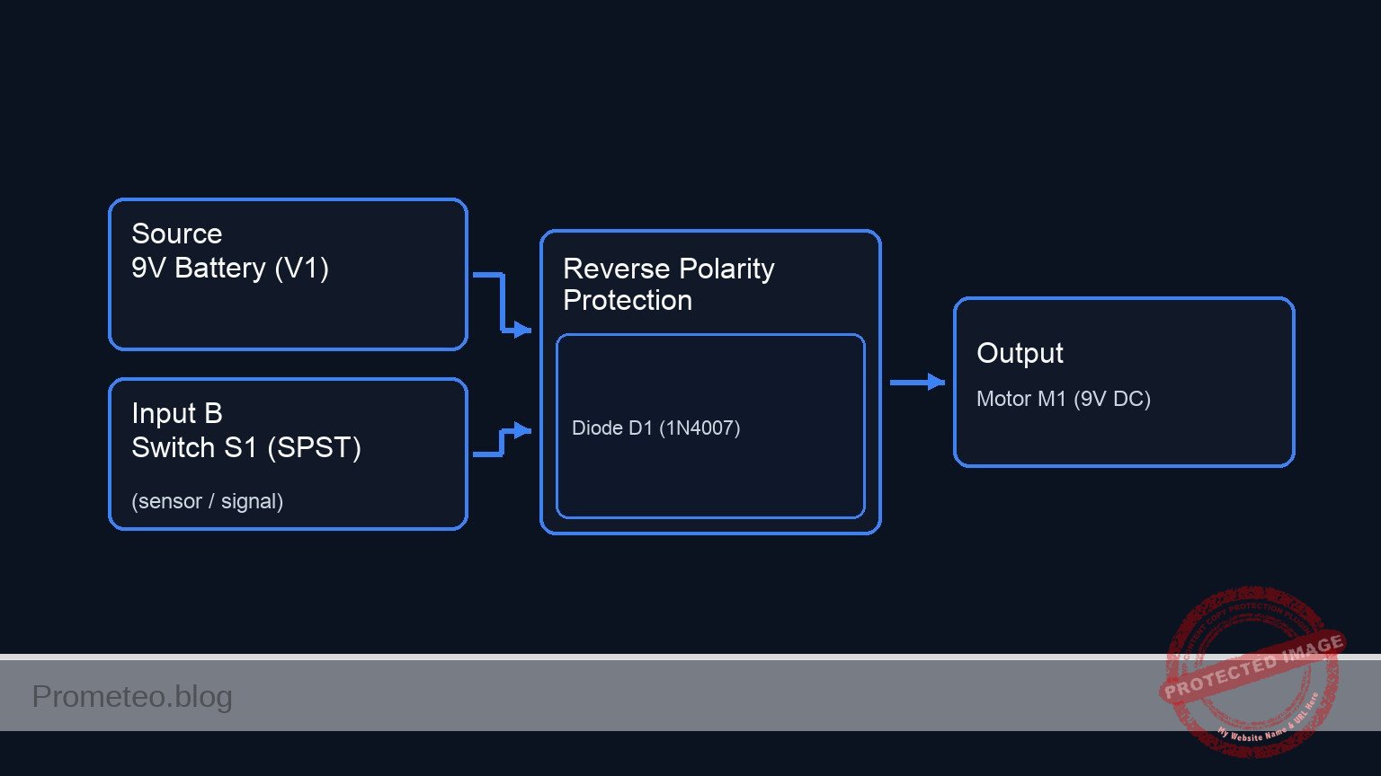
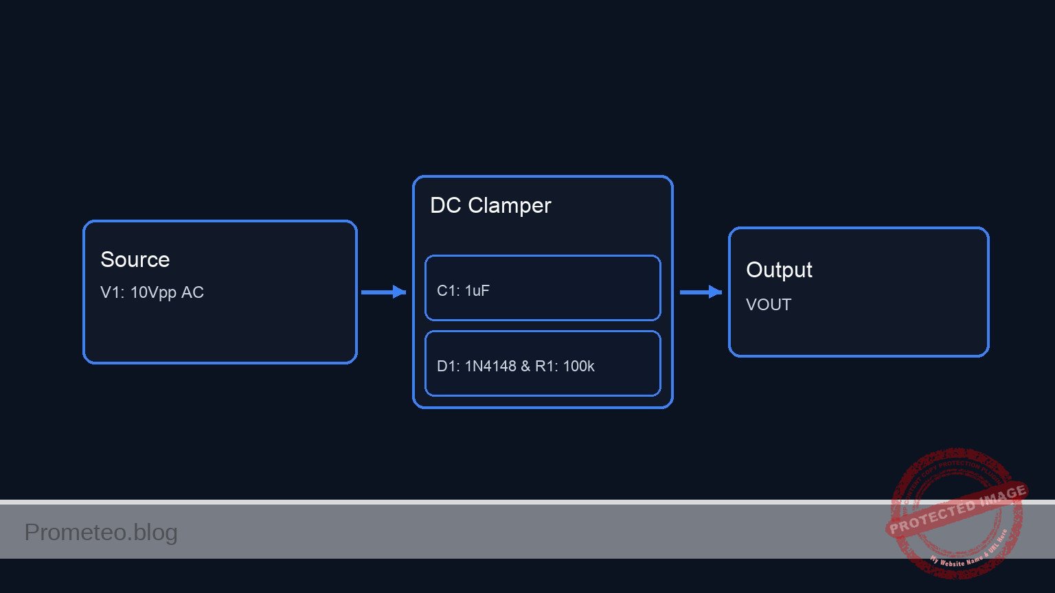
Materials

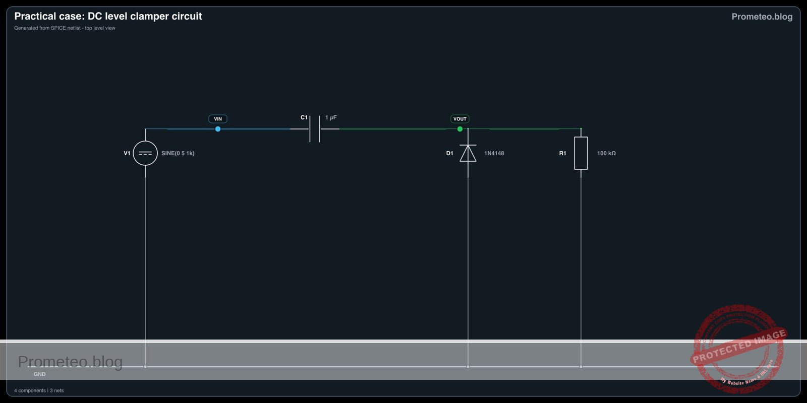
  • V1: 5 V peak (10 Vpp) 1 kHz AC sine wave source, function: input signal
  • C1: 1 µF capacitor, function: AC coupling and DC offset storage
  • D1: 1N4148 small-signal diode, function: clamps the minimum voltage level
  • R1: 100 kΩ resistor, function: provides a discharge path and defines the load

Wiring guide

  • V1: connects between node VIN (positive) and node 0 (GND).
  • C1: connects between node VIN and node VOUT.
  • D1: connects between node 0 (anode) and node VOUT (cathode).
  • R1: connects between node VOUT and node 0 (GND).

Conceptual block diagram

Conceptual block diagram — DC Clamper
Quick read: inputs → main block → output (actuator or measurement). This summarizes the ASCII schematic below.

Schematic

[ V1: 10Vpp AC ] --(VIN)--> [ C1: 1µF ] --(VOUT)--+--> [ R1: 100 kΩ ] --> GND
                                                  |
                                                  +--> [ D1: 1N4148 Cathode ] --(Anode)--> GND
Electrical Schematic

Measurements and tests

  1. Signal Generation: Connect your function generator or AC source to provide a 10 Vpp sine wave at 1 kHz to node VIN.
  2. Input Verification: Probe node VIN with an oscilloscope channel (DC coupled). Verify the V_in_waveform swings symmetrically from -5 V to +5 V.
  3. Output Waveform: Probe node VOUT with a second oscilloscope channel (DC coupled). Observe the V_out_waveform. It should swing approximately from -0.7 V to +9.3 V.
  4. DC Offset Measurement: Switch your digital multimeter (DMM) to DC Voltage mode and measure node VOUT relative to node 0. You should read a positive DC_offset of approximately +4.3 V.
  5. Time Constant Check: Note how the output waveform maintains its shape. The high value of R1 ensures the capacitor does not discharge significantly between cycles.

SPICE netlist and simulation

Reference SPICE Netlist (ngspice)

* Practical case: DC level clamper circuit
.width out=256

* Input Signal: 5V peak (10Vpp), 1kHz sine wave
V1 VIN 0 SINE(0 5 1k)

* AC coupling and DC offset storage capacitor
C1 VIN VOUT 1u

* Clamping diode (Anode to GND, Cathode to VOUT)
D1 0 VOUT 1N4148

* Load resistor and discharge path
R1 VOUT 0 100k

* Standard 1N4148 diode model
.model 1N4148 D(IS=4.35E-9 N=1.906 BV=110 IBV=0.0001 RS=0.6458 CJO=1.20E-11 M=0.3333 VJ=0.75 TT=3.48E-9)

* Transient analysis for 5 milliseconds to capture 5 full cycles of the 1kHz signal
.tran 10u 5m

* Output directives (Input and Output nodes first)
.print tran V(VIN) V(VOUT)
.op
.end

Copy this content into a .cir file and run with ngspice.

Simulation Results (Transient Analysis)

Simulation Results (Transient Analysis)

Analysis: The input signal v(vin) is a 10Vpp sine wave centered at 0V. The output signal v(vout) is shifted upwards, with its minimum clamped to approximately -0.8V (the forward voltage drop of the 1N4148 diode) and its maximum reaching about 9.38V.
Show raw data table (509 rows)
Index   time            v(vin)          v(vout)
0	0.000000e+00	0.000000e+00	-2.62072e-15
1	1.000000e-07	3.141592e-03	3.141552e-03
2	1.768596e-07	5.556208e-03	5.556134e-03
3	3.305789e-07	1.038543e-02	1.038529e-02
4	6.380174e-07	2.004385e-02	2.004355e-02
5	1.252894e-06	3.936043e-02	3.935972e-02
6	2.482649e-06	7.799154e-02	7.798965e-02
7	4.942157e-06	1.552375e-01	1.552318e-01
8	9.861173e-06	3.095997e-01	3.095809e-01
9	1.969921e-05	6.172898e-01	6.172223e-01
10	2.969921e-05	9.276226e-01	9.274748e-01
11	3.969921e-05	1.234294e+00	1.234036e+00
12	4.969921e-05	1.536095e+00	1.535695e+00
13	5.969921e-05	1.831833e+00	1.831263e+00
14	6.969921e-05	2.120342e+00	2.119572e+00
15	7.969921e-05	2.400483e+00	2.399485e+00
16	8.969921e-05	2.671151e+00	2.669897e+00
17	9.969921e-05	2.931276e+00	2.929740e+00
18	1.096992e-04	3.179833e+00	3.177990e+00
19	1.196992e-04	3.415841e+00	3.413667e+00
20	1.296992e-04	3.638368e+00	3.635840e+00
21	1.396992e-04	3.846536e+00	3.843632e+00
22	1.496992e-04	4.039523e+00	4.036224e+00
23	1.596992e-04	4.216569e+00	4.212856e+00
... (485 more rows) ...

Common mistakes and how to avoid them

  • Reversing the diode polarity: Placing the diode with the cathode to GND will create a negative clamper instead of a positive one. Always double-check the black band (cathode) orientation on the physical diode.
  • Using too small of a load resistor (R1): If R1 is too small, the RC time constant will be shorter than the signal’s period, causing the capacitor to discharge too quickly and distorting the output waveform into a «shark fin» shape.
  • Using a polarized capacitor incorrectly: If you use an electrolytic capacitor for C1, the positive leg must face the side with the higher average DC voltage (in this positive clamper case, facing node VOUT).

Troubleshooting

  • Symptom: The output waveform is identical to the input waveform (centered at 0 V).
    • Cause: The diode D1 is open, disconnected, or the capacitor C1 is shorted.
    • Fix: Check diode continuity with a multimeter and ensure the capacitor is wired in series with the signal.
  • Symptom: The output waveform is flat at 0 V or -0.7 V.
    • Cause: The diode D1 is shorted to ground, or VOUT is accidentally tied directly to GND.
    • Fix: Inspect the breadboard wiring at node VOUT and replace the diode if it fails a diode-mode test.
  • Symptom: The DC level is correct, but the waveform has severe droop or tilt on the flat edges.
    • Cause: The RC time constant is too low for the 1 kHz frequency.
    • Fix: Increase the value of R1 (e.g., from 10 kΩ to 100 kΩ) or increase C1 to prevent premature discharge.

Possible improvements and extensions

  • Biased Clamper: Add a small DC voltage source (e.g., a 1.5 V battery) in series with the diode D1 (between the anode and GND) to clamp the signal to an arbitrary reference level other than -0.7 V.
  • Negative Clamper Conversion: Reverse the direction of D1 (anode to VOUT, cathode to 0) and observe how the entire AC waveform is shifted downward, sitting entirely below +0.7 V.

More Practical Cases on Prometeo.blog

Find this product and/or books on this topic on Amazon

Go to Amazon

As an Amazon Associate, I earn from qualifying purchases. If you buy through this link, you help keep this project running.

Quick Quiz

Question 1: What is the primary function of the positive diode clamper circuit described in the text?


Question 2: Which of the following is a practical application of the clamper circuit mentioned in the article?


Question 3: How does the peak-to-peak amplitude of the output AC waveform compare to the input AC waveform?


Question 4: How is the measurable DC offset at the output roughly calculated?


Question 5: What is the specific function of the 1 µF capacitor (C1) in this circuit?


Question 6: Which component is responsible for clamping the minimum voltage level in the circuit?


Question 7: According to the wiring guide, how is the diode (D1) connected?


Question 8: Based on the text, what type of operational amplifiers benefit from biased AC signals provided by this circuit?


Question 9: What is the baseline of the incoming AC signal before it passes through the positive diode clamper?


Question 10: The positive diode clamper circuit is considered a foundational building block for which of the following?


Carlos Núñez Zorrilla
Electronics & Computer Engineer

Telecommunications Electronics Engineer and Computer Engineer (official degrees in Spain).

Follow me:


Practical case: Half-wave voltage doubler

Half-wave voltage doubler prototype (Maker Style)

Level: Medium | Objective: Analyze and assemble a voltage doubler circuit to increase the peak voltage of an AC signal.

Objective and use case

In this practical case, you will build a half-wave voltage doubler (a basic Villard/Greinacher cascade) using two diodes and two capacitors. This circuit rectifies an AC input while simultaneously stepping up the voltage, yielding a DC output roughly twice the peak voltage of the AC source.

Why this circuit is useful in the real world:
* Generating high-voltage bias supplies for components like vacuum tubes, cathode ray tubes, or photomultipliers.
* Providing higher voltage rails for specific operational amplifier stages without requiring a custom, bulky step-up transformer.
* Powering low-current electrostatic devices, ionizers, or Geiger-Müller tubes.

Expected outcome:
* The input signal (V_in_AC) operates as a standard sinusoidal wave.
* The output voltage (V_out_DC) measures approximately 2 × Vpeak of the input signal, minus the forward voltage drops of the two diodes.
* Ripple voltage will be present on the DC output and will noticeably increase when a heavier load (lower resistance) is connected.

Target audience: Intermediate electronics students learning AC-to-DC conversion and fundamental multiplier topologies.

Materials

  • V1: 12 Vrms (approx 17 Vpeak) AC source, 50/60 Hz, function: main AC input signal
  • D1: 1N4007 rectifier diode, function: first clamping stage
  • D2: 1N4007 rectifier diode, function: second peak rectifier stage
  • C1: 100 µF / 50 V electrolytic capacitor, function: AC coupling and intermediate charge storage
  • C2: 100 µF / 50 V electrolytic capacitor, function: output smoothing and final charge storage
  • R1: 10 kΩ resistor, function: light output load to safely discharge capacitors after power off

Wiring guide

  • V1: connects between node NODE_AC and node 0 (GND).
  • C1: connects between node NODE_AC (negative terminal) and node NODE_MID (positive terminal).
  • D1: connects between node 0 (anode) and node NODE_MID (cathode).
  • D2: connects between node NODE_MID (anode) and node VOUT (cathode).
  • C2: connects between node VOUT (positive terminal) and node 0 (negative terminal).
  • R1: connects between node VOUT and node 0.

Conceptual block diagram

Conceptual block diagram — Half-Wave Voltage Doubler
Quick read: inputs → main block → output (actuator or measurement). This summarizes the ASCII schematic below.

Schematic

GND
                                                        |
                                                  [ D1: 1N4007 ]
                                                        |
                                                        v
GND --> [ V1: 12Vrms AC ] --(NODE_AC)--> [ C1: 100µF ] --(NODE_MID)--> [ D2: 1N4007 ] --(VOUT)--> [ R1: 10 kΩ ] --> GND
                                                                                            |
                                                                                            +---> [ C2: 100µF ] --> GND
Electrical Schematic

Measurements and tests

  1. Measure the AC Input Peak: Connect an oscilloscope or a multimeter (in AC mode) across node NODE_AC and node 0. A 12 Vrms input should read roughly 17 V peak.
  2. Measure the Intermediate DC Voltage: Place a multimeter (in DC mode) across C1. You should read approximately Vpeak – 0.7 V (around 16.3 VDC).
  3. Measure the Doubled Output (V_out_DC): Probe between VOUT and 0 in DC mode. The voltage should be approximately 2 × Vpeak – 1.4 V (around 32.6 VDC).
  4. Observe Output Ripple: Switch the oscilloscope to AC coupling and probe VOUT. You will observe a ripple wave matching the frequency of the input source (half-wave rectification).
  5. Test Load Dependency: Swap R1 for a 1 kΩ resistor. Notice how the output DC voltage sags and the ripple amplitude increases significantly, proving this topology is best suited for low-current applications.

SPICE netlist and simulation

Reference SPICE Netlist (ngspice) — excerptFull SPICE netlist (ngspice)

* Practical case: Half-wave voltage doubler
.width out=256

* Main AC Input Signal (12 Vrms -> ~16.97 Vpeak, 50 Hz)
V1 NODE_AC 0 SIN(0 16.97056 50)

* AC coupling and intermediate charge storage
* Connected with NODE_MID as positive and NODE_AC as negative terminal
C1 NODE_MID NODE_AC 100u

* First clamping stage rectifier diode
D1 0 NODE_MID 1N4007

* Second peak rectifier stage diode
D2 NODE_MID VOUT 1N4007

* Output smoothing and final charge storage
C2 VOUT 0 100u

* Light output load to safely discharge capacitors
* ... (truncated in public view) ...

Copy this content into a .cir file and run with ngspice.

🔒 Part of this section is premium. With the 7-day pass or the monthly membership you can access the full content (materials, wiring, detailed build, validation, troubleshooting, variants and checklist) and download the complete print-ready PDF pack.

* Practical case: Half-wave voltage doubler
.width out=256

* Main AC Input Signal (12 Vrms -> ~16.97 Vpeak, 50 Hz)
V1 NODE_AC 0 SIN(0 16.97056 50)

* AC coupling and intermediate charge storage
* Connected with NODE_MID as positive and NODE_AC as negative terminal
C1 NODE_MID NODE_AC 100u

* First clamping stage rectifier diode
D1 0 NODE_MID 1N4007

* Second peak rectifier stage diode
D2 NODE_MID VOUT 1N4007

* Output smoothing and final charge storage
C2 VOUT 0 100u

* Light output load to safely discharge capacitors
R1 VOUT 0 10k

* Diode Model for 1N4007
.model 1N4007 D(IS=7.02767n RS=0.0341512 N=1.80803 EG=1.05743 XTI=5 BV=1000 IBV=5e-08 CJO=1e-11 VJ=0.7 M=0.5 FC=0.5 TT=1e-07)

* Simulation Directives
.print tran V(NODE_AC) V(VOUT) V(NODE_MID)
.tran 100u 500m
.op
.end
* --- GPT review (BOM/Wiring/SPICE) ---
* circuit_ok=true
* simulation_summary: The simulation shows the input AC voltage swinging between approximately -17V and +17V. The intermediate node (NODE_MID) is clamped and shifted, reaching a peak of about 32.6V. The output voltage (VOUT) successfully charges up to approximately 32V, which is nearly double the peak input voltage, confirming the voltage doubler operation.
* overall_comment: The SPICE netlist perfectly matches the BOM and wiring guide. The simulation results clearly demonstrate the expected behavior of a half-wave voltage doubler, with the output voltage reaching approximately twice the peak input voltage. This is an excellent didactic example.
* --------------------------------------

Simulation Results (Transient Analysis)

Simulation Results (Transient Analysis)

Analysis: The simulation shows the input AC voltage swinging between approximately -17V and +17V. The intermediate node (NODE_MID) is clamped and shifted, reaching a peak of about 32.6V. The output voltage (VOUT) successfully charges up to approximately 32V, which is nearly double the peak input voltage, confirming the voltage doubler operation.
Show raw data table (5027 rows)
Index   time            v(node_ac)      v(vout)         v(node_mid)
0	0.000000e+00	0.000000e+00	2.565925e-21	-1.89144e-18
1	1.000000e-06	5.331459e-03	5.419582e-10	5.331457e-03
2	2.000000e-06	1.066292e-02	1.097125e-09	1.066291e-02
3	4.000000e-06	2.132583e-02	2.236679e-09	2.132582e-02
4	8.000000e-06	4.265162e-02	4.716739e-09	4.265162e-02
5	1.600000e-05	8.530298e-02	1.109752e-08	8.530296e-02
6	2.994581e-05	1.596525e-01	3.640348e-08	1.596524e-01
7	4.360349e-05	2.324629e-01	1.285942e-07	2.324628e-01
8	5.923389e-05	3.157848e-01	6.926674e-07	3.157841e-01
9	7.569182e-05	4.035098e-01	4.463881e-06	4.035053e-01
10	9.313209e-05	4.964590e-01	3.310357e-05	4.964259e-01
11	1.114841e-04	5.942514e-01	2.714571e-04	5.939798e-01
12	1.306697e-04	6.964642e-01	2.279240e-03	6.941849e-01
13	1.507869e-04	8.036134e-01	1.447578e-02	7.891374e-01
14	1.727320e-04	9.204617e-01	5.134539e-02	8.691153e-01
15	1.929217e-04	1.027924e+00	1.015818e-01	9.263400e-01
16	2.144482e-04	1.142457e+00	1.586780e-01	9.837739e-01
17	2.454175e-04	1.307137e+00	2.410344e-01	1.066092e+00
18	2.845422e-04	1.515006e+00	3.449894e-01	1.169993e+00
19	3.627917e-04	1.930024e+00	5.525467e-01	1.377419e+00
20	4.627917e-04	2.458671e+00	8.169450e-01	1.641599e+00
21	5.627917e-04	2.984892e+00	1.080147e+00	1.904524e+00
22	6.627917e-04	3.508167e+00	1.341889e+00	2.165935e+00
23	7.627917e-04	4.027980e+00	1.601917e+00	2.425574e+00
... (5003 more rows) ...

Common mistakes and how to avoid them

  • Reversing diode polarity: Installing D1 or D2 backward will either clamp the voltage to a negative potential instead of positive, or block the charge from reaching the output entirely. Always check the silver band indicating the cathode.
  • Incorrect capacitor polarity: Electrolytic capacitors will fail or vent if reverse-biased. Ensure C1‘s positive terminal faces the diode junction (NODE_MID) and C2‘s positive terminal faces VOUT.
  • Using capacitors with low voltage ratings: C2 must handle the fully doubled voltage (2 × Vpeak). Using a 25 V capacitor for a 34 V output will cause immediate failure. Always select capacitors rated for at least 2.5 × Vpeak of the AC source.

Troubleshooting

  • Symptom: Output voltage is only equal to Vpeak (not doubled).
    • Cause: C1 is shorted, or D1 is open/damaged.
    • Fix: Verify D1‘s continuity using a multimeter diode test and check C1 for internal shorts.
  • Symptom: Output voltage (VOUT) is zero or close to zero.
    • Cause: D2 is installed backwards (blocking the DC flow), or the load resistor R1 is completely shorted/too small, collapsing the multiplier’s charge.
    • Fix: Verify D2 orientation and ensure R1 is at least 10 kΩ for testing.
  • Symptom: Loud pop or bulging capacitor upon power-up.
    • Cause: C2 voltage rating was exceeded or it was connected with reversed polarity.
    • Fix: Immediately disconnect power. Replace the damaged capacitor, double-checking correct polarity and a safe voltage rating (e.g., ≥ 50 V).

Possible improvements and extensions

  • Add multiplier stages: Cascade additional diodes and capacitors to turn this circuit into a Cockcroft-Walton voltage tripler or quadrupler for even higher DC potentials.
  • Build a full-wave voltage doubler: Reconfigure the circuit into a full-wave doubler topology to double the ripple frequency, which reduces the required size of the filter capacitors to maintain a stable output under load.

More Practical Cases on Prometeo.blog

Find this product and/or books on this topic on Amazon

Go to Amazon

As an Amazon Associate, I earn from qualifying purchases. If you buy through this link, you help keep this project running.

Quick Quiz

Question 1: What type of circuit is being built in this practical case?


Question 2: What are the primary components required to build this voltage doubler?


Question 3: What is the expected DC output voltage of this circuit?


Question 4: Which of the following is a real-world application for a voltage doubler?


Question 5: What happens to the theoretical output voltage due to the diodes in the circuit?


Question 6: How does a heavier load (lower resistance) affect the DC output?


Question 7: What type of input signal is used in this practical case?


Question 8: Why might a voltage doubler be preferred over a step-up transformer for certain op-amp stages?


Question 9: Which specific cascade topology is mentioned as the basis for this half-wave voltage doubler?


Question 10: What type of devices are suitable to be powered by this circuit due to its low-current characteristics?


Carlos Núñez Zorrilla
Electronics & Computer Engineer

Telecommunications Electronics Engineer and Computer Engineer (official degrees in Spain).

Follow me:


Practical case: Zener Diode as a Voltage Regulator

Zener Diode as a Voltage Regulator prototype (Maker Style)

Level: Medium. Design and verify a voltage stabilizer circuit using a Zener diode under load variations.

Objective and use case

In this session, you will build a shunt voltage regulator using a Zener diode and a series limiting resistor to maintain a fixed 5.1 V output from a 9 V source.

  • Why it is useful:
    • Provides a stable reference voltage for Analog-to-Digital Converters (ADCs).
    • Protects sensitive downstream components (like microcontrollers) from over-voltage spikes.
    • Regulates voltage for low-power circuits without the complexity of an IC regulator.
  • Expected outcome:
    • The output voltage (VOUT) remains clamped at approximately 5.1 V despite the input being 9 V.
    • Connecting a moderate load (470 Ω) decreases Zener current but maintains VOUT at 5.1 V.
    • If the load resistance becomes too low, the regulation fails, and VOUT drops below 5.1 V.
  • Target audience: Electronics students, Level: Medium.

Materials

  • V1: 9 V DC voltage source, function: main power supply.
  • R1: 220 Ω resistor, function: series current limiting (RS).
  • D1: 1N4733 A Zener diode (5.1 V, 1 W), function: shunt voltage regulator.
  • R2: 470 Ω resistor, function: load simulation (RL).
  • M1: Multimeter (Voltmeter mode), function: measure output voltage.
  • M2: Multimeter (Ammeter mode), function: measure Zener current (IZ).

Wiring guide

Construct the circuit using the following connections and SPICE node names (VIN, VOUT, 0):

  • V1 (9 V Supply): Connect Positive terminal to node VIN and Negative terminal to node 0 (GND).
  • R1 (Series Resistor): Connect one terminal to VIN and the other terminal to node VOUT.
  • D1 (Zener Diode): Connect the Cathode (striped end) to node VOUT and the Anode to node 0.
  • R2 (Load Resistor): Connect one terminal to VOUT and the other terminal to node 0.
  • Measurements:
    • To measure VOUT: Connect the Voltmeter Positive probe to VOUT and Negative probe to 0.
    • To measure IZ: Break the connection between D1 Cathode and VOUT, and insert the Ammeter in series (Positive to VOUT, Negative to D1 Cathode).

Conceptual block diagram

Conceptual block diagram — Zener Voltage Regulator
Quick read: inputs → main block → output (actuator or measurement). This summarizes the ASCII schematic below.

Schematic

[ SOURCE ]                 [ LIMITING ]                     [ REGULATION, LOAD & MEASUREMENT ]

                                                                           (Branch 1: Regulation)
                                                                 +---> [ Ammeter M2 ] --> [ D1: Zener 5.1 V ] --> GND
                                                                 |     (Measure Iz)       (Shunt Regulator)
                                                                 |
    [ V1: 9 V DC ] --(VIN)--> [ R1: 220 Ohm ] --(Node VOUT)--> ---+
    (Main Power)             (Series Resistor)                   |         (Branch 2: Load)
                                                                 +---> [ R2: 470 Ohm ] ------------------------> GND
                                                                 |     (Load Simulation)
                                                                 |
                                                                 |         (Branch 3: Monitoring)
                                                                 +---> [ Voltmeter M1 ] -----------------------> GND
                                                                       (Measure Vout)
Schematic (ASCII)

Measurements and tests

Follow these steps to validate the regulator design:

  1. Open Circuit Test (No Load):

    • Temporarily disconnect R2.
    • Measure voltage at VOUT. It should read approximately 5.1 V.
    • Calculate the current flowing through the Zener: IZ = (VIN – VZ) / R1. Expect ≈ 17.7 mA.
  2. Load Regulation Test:

    • Reconnect R2 (470 Ω) between VOUT and 0.
    • Measure VOUT again. It should remain stable at 5.1 V.
    • Observe the Zener current. It should decrease because some current is now diverted through the load RL.
    • Expected Load Current (IL): 5.1 V / 470 Ω ≈ 10.8 mA.
    • Remaining Zener Current: ≈ 17.7 mA – 10.8 mA = 6.9 mA. Since IZ > 0, regulation holds.
  3. Overload Test (Simulation):

    • Replace R2 with a 100 Ω resistor (if available) or simulate a short.
    • Measure VOUT. The voltage will drop significantly below 5.1 V because the load demands more current than R1 can supply while maintaining the Zener breakdown voltage.

SPICE netlist and simulation

Reference SPICE Netlist (ngspice) — excerptFull SPICE netlist (ngspice)

* Practical case: Zener Diode as a Voltage Regulator

* --- Power Supply ---
* V1: 9 V DC voltage source (Main Supply)
V1 VIN 0 DC 9

* --- Components ---
* R1: 220 Ohm Resistor (Series Current Limiting)
* Wiring: Connect one terminal to VIN and the other to VOUT
R1 VIN VOUT 220

* R2: 470 Ohm Resistor (Load Simulation)
* Wiring: Connect one terminal to VOUT and the other to 0 (GND)
R2 VOUT 0 470

* M1: Multimeter (Voltmeter mode)
* Wiring: Positive probe to VOUT, Negative probe to 0
* Implementation: High impedance resistor to simulate voltmeter load
R_M1_Voltmeter VOUT 0 10Meg

* ... (truncated in public view) ...

Copy this content into a .cir file and run with ngspice.

🔒 Part of this section is premium. With the 7-day pass or the monthly membership you can access the full content (materials, wiring, detailed build, validation, troubleshooting, variants and checklist) and download the complete print-ready PDF pack.

* Practical case: Zener Diode as a Voltage Regulator

* --- Power Supply ---
* V1: 9 V DC voltage source (Main Supply)
V1 VIN 0 DC 9

* --- Components ---
* R1: 220 Ohm Resistor (Series Current Limiting)
* Wiring: Connect one terminal to VIN and the other to VOUT
R1 VIN VOUT 220

* R2: 470 Ohm Resistor (Load Simulation)
* Wiring: Connect one terminal to VOUT and the other to 0 (GND)
R2 VOUT 0 470

* M1: Multimeter (Voltmeter mode)
* Wiring: Positive probe to VOUT, Negative probe to 0
* Implementation: High impedance resistor to simulate voltmeter load
R_M1_Voltmeter VOUT 0 10Meg

* M2: Multimeter (Ammeter mode)
* Wiring: Inserted in series between VOUT and D1 Cathode
* Positive to VOUT, Negative to D1 Cathode (Node: VZ_CATHODE)
* Implementation: 0V DC source to measure current
V_M2_Ammeter VOUT VZ_CATHODE DC 0

* D1: 1N4733A Zener Diode (5.1 V, 1 W)
* Wiring: Cathode to VZ_CATHODE, Anode to 0
* Note: Cathode is connected to VOUT through the Ammeter
D1 0 VZ_CATHODE D1N4733A

* --- Models ---
* Model for 1N4733A Zener Diode
* BV=5.1V (Breakdown Voltage), IBV=49mA (Test Current)
.model D1N4733A D(IS=2.5n RS=1 N=1.2 BV=5.1 IBV=49m)

* --- Analysis ---
* Transient analysis (1ms simulation time)
.tran 1u 1ms

* --- Output Directives ---
* Print voltages and Zener current (Iz)
.print tran V(VIN) V(VOUT) I(V_M2_Ammeter)

* Operating Point for initial check
.op

.end

Simulation Results (Transient Analysis)

Simulation Results (Transient Analysis)
Show raw data table (1008 rows)
Index   time            v(vin)          v(vout)         v_m2_ammeter#br
0	0.000000e+00	9.000000e+00	5.047821e+00	7.223902e-03
1	1.000000e-08	9.000000e+00	5.047805e+00	7.224007e-03
2	2.000000e-08	9.000000e+00	5.047805e+00	7.224007e-03
3	4.000000e-08	9.000000e+00	5.047805e+00	7.224007e-03
4	8.000000e-08	9.000000e+00	5.047805e+00	7.224007e-03
5	1.600000e-07	9.000000e+00	5.047805e+00	7.224007e-03
6	3.200000e-07	9.000000e+00	5.047805e+00	7.224007e-03
7	6.400000e-07	9.000000e+00	5.047805e+00	7.224007e-03
8	1.280000e-06	9.000000e+00	5.047805e+00	7.224007e-03
9	2.280000e-06	9.000000e+00	5.047805e+00	7.224007e-03
10	3.280000e-06	9.000000e+00	5.047805e+00	7.224007e-03
11	4.280000e-06	9.000000e+00	5.047805e+00	7.224007e-03
12	5.280000e-06	9.000000e+00	5.047805e+00	7.224007e-03
13	6.280000e-06	9.000000e+00	5.047805e+00	7.224007e-03
14	7.280000e-06	9.000000e+00	5.047805e+00	7.224007e-03
15	8.280000e-06	9.000000e+00	5.047805e+00	7.224007e-03
16	9.280000e-06	9.000000e+00	5.047805e+00	7.224007e-03
17	1.028000e-05	9.000000e+00	5.047805e+00	7.224007e-03
18	1.128000e-05	9.000000e+00	5.047805e+00	7.224007e-03
19	1.228000e-05	9.000000e+00	5.047805e+00	7.224007e-03
20	1.328000e-05	9.000000e+00	5.047805e+00	7.224007e-03
21	1.428000e-05	9.000000e+00	5.047805e+00	7.224007e-03
22	1.528000e-05	9.000000e+00	5.047805e+00	7.224007e-03
23	1.628000e-05	9.000000e+00	5.047805e+00	7.224007e-03
... (984 more rows) ...

Common mistakes and how to avoid them

  1. Reversing the Zener Diode:
    • Error: Connecting the Anode to VOUT and Cathode to GND.
    • Result: The circuit behaves like a standard diode, clamping the output to ≈ 0.7 V instead of 5.1 V.
    • Solution: Ensure the striped end (Cathode) is connected to the positive potential (VOUT).
  2. Using a Series Resistor (R1) with too high resistance:
    • Error: Using 10 kΩ instead of 220 Ω for R1.
    • Result: When the load (R2) is connected, the voltage drops immediately; the Zener turns off because there isn’t enough current to keep it in breakdown.
    • Solution: Calculate R1 such that enough current flows to satisfy both the load and the minimum Zener bias current (IZK).
  3. Exceeding Zener Power Rating:
    • Error: Removing the load while using a very small R1.
    • Result: All current flows through the Zener, causing it to overheat and potentially burn out.
    • Solution: Ensure PZ = VZ × Izmax is less than the diode’s power rating (e.g., 1 W).

Troubleshooting

  • Symptom: Output voltage is equal to Input voltage (9 V).
    • Cause: Zener diode is open (broken) or not connected.
    • Fix: Check connections to D1 or replace the diode.
  • Symptom: Output voltage is ≈ 0.7 V.
    • Cause: Zener diode is connected in forward bias (backwards).
    • Fix: Reverse the diode orientation.
  • Symptom: Output is 5.1 V without load, but drops to 3 V (or lower) when load is attached.
    • Cause: The load resistance is too low (drawing too much current) or R1 is too high.
    • Fix: Increase the load resistance or recalculate R1 for higher current delivery (watching power limits).

Possible improvements and extensions

  1. Series Pass Transistor: Add an NPN transistor (like a 2N2222) with the Zener controlling the base. This creates a Series Voltage Regulator capable of handling much higher load currents.
  2. Filtering: Add a capacitor (e.g., 10 µF) in parallel with the Zener diode to filter out noise and improve the stability of the voltage reference.

More Practical Cases on Prometeo.blog

Find this product and/or books on this topic on Amazon

Go to Amazon

As an Amazon Associate, I earn from qualifying purchases. If you buy through this link, you help keep this project running.

Quick Quiz

Question 1: What is the primary function of the Zener diode in the described circuit?


Question 2: What is the expected output voltage (VOUT) of this circuit when functioning correctly?


Question 3: Which component is responsible for limiting the current flowing through the Zener diode?


Question 4: How must the Zener diode be biased in this circuit to regulate voltage?


Question 5: What happens to the Zener current when a moderate load (470 Ω) is connected in parallel?


Question 6: Under what condition does the voltage regulation of this circuit fail?


Question 7: Why is this circuit useful for Analog-to-Digital Converters (ADCs)?


Question 8: Which specific Zener diode model is specified in the materials list?


Question 9: What is the primary purpose of the 9 V DC source (V1) in this setup?


Question 10: Besides providing a reference voltage, what is another key use case for this circuit?


Carlos Núñez Zorrilla
Electronics & Computer Engineer

Telecommunications Electronics Engineer and Computer Engineer (official degrees in Spain).

Follow me:


Practical case: Full-wave bridge rectifier

Full-wave bridge rectifier prototype (Maker Style)

Level: Medium – Analyze a Graetz bridge to convert AC to pulsating DC and measure total voltage drop.

Objective and use case

In this practical case, you will build a standard Graetz bridge circuit using four diodes and an AC voltage source to supply a resistive load. This circuit converts an alternating current input (where voltage polarity changes) into a pulsating direct current output (where voltage polarity remains positive).

Why it is useful:
* Power Supplies: It is the fundamental first stage in converting AC mains power to DC for charging laptops, phones, and powering appliances.
* Motor Control: Used in DC motor drives to run motors from an AC supply.
* Polarity Protection: Ensures that a device works correctly regardless of how the input power wires are connected.
* High Efficiency: Utilizes both the positive and negative half-cycles of the AC input, unlike a half-wave rectifier.

Expected outcome:
* Input Signal: A sinusoidal waveform (e.g., 12 V RMS / ~17 V Peak) at 60Hz.
* Output Signal: A series of positive «mounds» (pulsating DC) at 120Hz (double the input frequency).
* Voltage Drop: The peak output voltage will be approximately 1.4 V lower than the peak input voltage due to the forward voltage drop of two diodes in series (2 × 0.7 V).
* Current Flow: Current flows through the load resistor in the same direction during both AC half-cycles.

Target audience and level: Electronics students and hobbyists familiar with basic diode biasing.

Materials

  • V1: AC Voltage Source (Amplitude: 17 V [12Vrms], Frequency: 60Hz), function: Input supply
  • D1: 1N4007 Diode, function: Rectifier (Bridge arm 1)
  • D2: 1N4007 Diode, function: Rectifier (Bridge arm 2)
  • D3: 1N4007 Diode, function: Rectifier (Bridge arm 3)
  • D4: 1N4007 Diode, function: Rectifier (Bridge arm 4)
  • R1: 1 kΩ resistor, function: Output Load

Wiring guide

This guide uses specific node names to represent the connections. Ensure the AC source is floating relative to the DC ground to simulate the isolation provided by a transformer.

  • V1 (Positive terminal) connects to node AC1.
  • V1 (Negative terminal) connects to node AC2.
  • D1 (Anode) connects to node AC1.
  • D1 (Cathode) connects to node VOUT.
  • D2 (Anode) connects to node AC2.
  • D2 (Cathode) connects to node VOUT.
  • D3 (Anode) connects to node 0 (GND).
  • D3 (Cathode) connects to node AC1.
  • D4 (Anode) connects to node 0 (GND).
  • D4 (Cathode) connects to node AC2.
  • R1 connects between node VOUT and node 0 (GND).

Conceptual block diagram

Conceptual block diagram — LM7812 Full-Wave Bridge Rectifier
Quick read: inputs → main block → output (actuator or measurement). This summarizes the ASCII schematic below.

Schematic

[ INPUT SOURCE ]               [ PROCESSING / LOGIC ]               [ OUTPUT LOAD ]

[ AC Source V1 ]
(17 V Amp / 60Hz)
       |
       +----(Node AC1)----->+-----------------------------+
                            |    FULL-WAVE BRIDGE         |
                            |                             |
                            |  [ Diodes D1 & D2 ]         |
                            |  (Direct Positive Peaks)    |--(Node VOUT)--> [ Resistor R1 ]
                            |                             |                 (1 kOhm)
                            |                             |                     |
       +----(Node AC2)----->|  [ Diodes D3 & D4 ]         |                     |
       |                    |  (Direct Negative Peaks)    |                     v
       |                    |  (Create Return Path)       |                    GND
(Source Return)             |                             |
                            +-----------------------------+
                                          |
                                          v
                                     (Node 0/GND)
Schematic (ASCII)

Measurements and tests

Perform the following steps to validate the circuit operation using an oscilloscope or a multimeter:

  1. Input Verification: Connect channel 1 of the oscilloscope across AC1 and AC2. Verify a full sine wave with a frequency of 60Hz.
  2. Output Visualization: Connect channel 2 of the oscilloscope across R1 (Probe on VOUT, Clip on 0). Observe that the negative portions of the sine wave have been «flipped» up, creating a continuous chain of positive pulses.
  3. Frequency Measurement: Measure the frequency of the signal at VOUT. It should be exactly 120Hz (double the input frequency).
  4. Voltage Drop Analysis: Measure the peak voltage of the Input (Vpeakin) and the peak voltage of the Output (Vpeakout).
    • Vpeakout should be approximately Vpeakin – 1.4 V. This accounts for the 0.7 V drop across D1 and 0.7 V drop across D4 (during one cycle) or D2 and D3 (during the other).

SPICE netlist and simulation

Reference SPICE Netlist (ngspice) — excerptFull SPICE netlist (ngspice)

* Title: Practical case: Full-wave bridge rectifier

* --- Component Instantiation ---

* V1: AC Voltage Source (Amplitude: 17 V, Frequency: 60Hz)
* Wiring: V1 (Positive) -> AC1, V1 (Negative) -> AC2
* Note: Source is floating relative to ground (Node 0), connected only to the bridge.
V1 AC1 AC2 SIN(0 17 60)

* D1: 1N4007 Diode (Bridge arm 1)
* Wiring: Anode -> AC1, Cathode -> VOUT
D1 AC1 VOUT 1N4007

* D2: 1N4007 Diode (Bridge arm 2)
* Wiring: Anode -> AC2, Cathode -> VOUT
D2 AC2 VOUT 1N4007

* D3: 1N4007 Diode (Bridge arm 3)
* Wiring: Anode -> 0 (GND), Cathode -> AC1
D3 0 AC1 1N4007
* ... (truncated in public view) ...

Copy this content into a .cir file and run with ngspice.

🔒 Part of this section is premium. With the 7-day pass or the monthly membership you can access the full content (materials, wiring, detailed build, validation, troubleshooting, variants and checklist) and download the complete print-ready PDF pack.

* Title: Practical case: Full-wave bridge rectifier

* --- Component Instantiation ---

* V1: AC Voltage Source (Amplitude: 17 V, Frequency: 60Hz)
* Wiring: V1 (Positive) -> AC1, V1 (Negative) -> AC2
* Note: Source is floating relative to ground (Node 0), connected only to the bridge.
V1 AC1 AC2 SIN(0 17 60)

* D1: 1N4007 Diode (Bridge arm 1)
* Wiring: Anode -> AC1, Cathode -> VOUT
D1 AC1 VOUT 1N4007

* D2: 1N4007 Diode (Bridge arm 2)
* Wiring: Anode -> AC2, Cathode -> VOUT
D2 AC2 VOUT 1N4007

* D3: 1N4007 Diode (Bridge arm 3)
* Wiring: Anode -> 0 (GND), Cathode -> AC1
D3 0 AC1 1N4007

* D4: 1N4007 Diode (Bridge arm 4)
* Wiring: Anode -> 0 (GND), Cathode -> AC2
D4 0 AC2 1N4007

* R1: 1 kΩ Resistor (Output Load)
* Wiring: VOUT -> 0 (GND)
R1 VOUT 0 1k

* --- Models ---
* Standard model for 1N4007 Rectifier Diode
.model 1N4007 D (IS=7.03n RS=0.034 N=1.81 BV=1000 IBV=0.5u CJO=10p TT=0.1u)

* --- Analysis Commands ---
* Transient analysis: 60Hz period is ~16.6ms.
* Simulating 50ms to capture approximately 3 full cycles.
.tran 50u 50m

* --- Output Directives ---
* Print voltages at AC inputs (relative to GND) and the rectified Output
.print tran V(AC1) V(AC2) V(VOUT)

* Calculate DC operating point
.op

.end

Simulation Results (Transient Analysis)

Simulation Results (Transient Analysis)
Show raw data table (1016 rows)
Index   time            v(ac1)          v(ac2)          v(vout)
0	0.000000e+00	3.036573e-18	3.036573e-18	-7.53268e-22
1	5.000000e-07	1.602212e-03	-1.60221e-03	-9.54567e-15
2	1.000000e-06	3.204481e-03	-3.20437e-03	1.126318e-07
3	2.000000e-06	6.409036e-03	-6.40866e-03	3.747988e-07
4	4.000000e-06	1.281816e-02	-1.28172e-02	9.375665e-07
5	8.000000e-06	2.563689e-02	-2.56338e-02	3.056599e-06
6	1.600000e-05	5.127600e-02	-5.12650e-02	1.103556e-05
7	3.200000e-05	1.025657e-01	-1.02513e-01	5.319168e-05
8	6.400000e-05	2.053399e-01	-2.04787e-01	5.532611e-04
9	1.140000e-04	3.725509e-01	-3.57833e-01	1.471794e-02
10	1.640000e-04	5.903791e-01	-4.60003e-01	1.303764e-01
11	2.140000e-04	8.628382e-01	-5.07168e-01	3.556700e-01
12	2.640000e-04	1.155738e+00	-5.33407e-01	6.223310e-01
13	3.140000e-04	1.456815e+00	-5.50867e-01	9.059481e-01
14	3.640000e-04	1.761378e+00	-5.64128e-01	1.197250e+00
15	4.140000e-04	2.068103e+00	-5.74401e-01	1.493702e+00
16	4.640000e-04	2.375673e+00	-5.82891e-01	1.792782e+00
17	5.140000e-04	2.683430e+00	-5.90142e-01	2.093289e+00
18	5.640000e-04	2.990978e+00	-5.96439e-01	2.394538e+00
19	6.140000e-04	3.297988e+00	-6.02000e-01	2.695989e+00
20	6.640000e-04	3.604206e+00	-6.06966e-01	2.997240e+00
21	7.140000e-04	3.909408e+00	-6.11453e-01	3.297955e+00
22	7.640000e-04	4.213406e+00	-6.15537e-01	3.597869e+00
23	8.140000e-04	4.516026e+00	-6.19284e-01	3.896742e+00
... (992 more rows) ...

Common mistakes and how to avoid them

  1. Ground Loops (Scope): Connecting the oscilloscope ground clip to AC1 or AC2 while the circuit is mains-referenced can cause a short circuit. Solution: Only connect the scope ground to the common circuit ground (0) at the load, or use a differential probe for the input.
  2. Diode Orientation: Inserting a diode backward in the bridge. Solution: Ensure that two diodes point towards the positive DC output node (VOUT) and two diodes point away from the ground node (0).
  3. Ignoring Power Ratings: Using a resistor with low wattage for R1. Solution: Calculate power P = V^2 / R. For 17 V peak, P ≈ 0.3W. Use a 0.5W resistor or greater.

Troubleshooting

  • Symptom: The output looks like a half-wave rectifier (gaps between pulses).
    • Cause: One of the diodes is open (disconnected or blown).
    • Fix: Check continuity of all four diodes; replace the faulty one.
  • Symptom: Zero output voltage.
    • Cause: Short circuit in the load or open circuit in the source/wiring.
    • Fix: Check connections at AC1 and AC2; ensure R1 is not shorted.
  • Symptom: Input fuse blows or source current is excessive.
    • Cause: One or more diodes are shorted, or a diode is installed in reverse (creating a direct path from AC to Ground).
    • Fix: Test diodes for shorts using the diode check mode on a multimeter.

Possible improvements and extensions

  1. Filtering: Add a capacitor (e.g., 470 µF) in parallel with R1 to fill in the gaps between pulses, creating a smooth DC voltage (Ripple reduction).
  2. Regulation: Connect a voltage regulator (like an LM7812 or a Zener diode circuit) after the filter capacitor to produce a constant, stable DC voltage regardless of input fluctuations.

More Practical Cases on Prometeo.blog

Find this product and/or books on this topic on Amazon

Go to Amazon

As an Amazon Associate, I earn from qualifying purchases. If you buy through this link, you help keep this project running.

Quick Quiz

Question 1: What is the primary function of a Graetz bridge circuit?


Question 2: How many diodes are typically used to build a standard Graetz bridge?


Question 3: Why is the Graetz bridge considered more efficient than a half-wave rectifier?


Question 4: If the input AC frequency is 60Hz, what is the frequency of the pulsating DC output in a Graetz bridge?


Question 5: What is the approximate total voltage drop expected at the peak output compared to the peak input?


Question 6: Why does the voltage drop occur in this circuit?


Question 7: Which component serves as the rectifying element in the described circuit?


Question 8: What happens to the direction of current flow through the load resistor during the negative half-cycle of the AC input?


Question 9: If the input source provides 12 V RMS, what is the approximate peak voltage amplitude mentioned in the text?


Question 10: Besides power supplies, what is another use case mentioned for the Graetz bridge?


Carlos Núñez Zorrilla
Electronics & Computer Engineer

Telecommunications Electronics Engineer and Computer Engineer (official degrees in Spain).

Follow me:


Practical case: Voltage limiter with series diodes

Voltage limiter with series diodes prototype (Maker Style)

Level: Basic – Build a circuit to clamp load voltage using diode forward drops.

Objective and use case

In this practical case, you will build a passive voltage limiter (clipper) circuit. By placing multiple silicon diodes in series parallel to the load, you will create a hard «ceiling» for the output voltage, preventing it from exceeding the sum of the forward voltage drops of the diodes.

  • Input protection: Prevents high voltage spikes from damaging sensitive microcontroller inputs (ADCs).
  • Simple regulation: Provides a crude but effective constant voltage reference without a Zener diode.
  • Signal conditioning: Used in audio circuits to create distortion or «fuzz» effects by clipping signal peaks.
  • Logical reference: Can be used to establish specific logic threshold levels in analog computing.

Expected outcome:
* When Input Voltage < ~2.1 V: The output voltage follows the input (minus minor resistive losses).
* When Input Voltage > ~2.1 V: The output voltage clamps and remains stable at approximately 2.1 V.
* The current through the diodes increases significantly once the threshold is reached.
* Target audience: Students and hobbyists learning about diode I-V characteristics.

Materials

  • V1: 0 V to 9 V Variable DC Power Supply, function: Input signal source.
  • R1: 1 kΩ resistor, function: Current limiting for the diodes and source protection.
  • R2: 10 kΩ resistor, function: Load resistor (simulating a downstream circuit).
  • D1: 1N4148 Silicon Diode, function: First voltage drop element (~0.7 V).
  • D2: 1N4148 Silicon Diode, function: Second voltage drop element (~0.7 V).
  • D3: 1N4148 Silicon Diode, function: Third voltage drop element (~0.7 V).

Wiring guide

Construct the circuit following these connections. The node names (e.g., VIN, VOUT, 0) refer to specific electrical points in the circuit. Node 0 represents the Ground (GND).

  • V1 (Source): Connect the positive terminal to node VIN and the negative terminal to node 0.
  • R1 (Limiter): Connect one pin to node VIN and the other pin to node VOUT.
  • R2 (Load): Connect one pin to node VOUT and the other pin to node 0.
  • D1: Connect the Anode to node VOUT and the Cathode to intermediate node N1.
  • D2: Connect the Anode to intermediate node N1 and the Cathode to intermediate node N2.
  • D3: Connect the Anode to intermediate node N2 and the Cathode to node 0.

Note: This creates a chain where D1, D2, and D3 are in series with each other, and that entire string is in parallel with R2.

Conceptual block diagram

Conceptual block diagram — Series Diode Limiter
Quick read: inputs → main block → output (actuator or measurement). This summarizes the ASCII schematic below.

Schematic

[ INPUT SOURCE ]              [ SERIES LIMITER ]                  [ OUTPUT NODE & BRANCHES ]

                                                                 /------> [ R2: 10 kΩ Load ] ---------> GND (0)
                                                                 |
[ V1: 0-9 V Variable ] --(VIN)--> [ R1: 1 kΩ Resistor ] --(VOUT)-->+
                                                                 |
                                                                 |        [ VOLTAGE CLAMP CHAIN ]
                                                                 |
                                                                 \------> [ D1: 1N4148 ] --(N1)-->+
                                                                                                  |
                                                                          [ D2: 1N4148 ] <--------+
                                                                          |
                                                                          +--(N2)--> [ D3: 1N4148 ] --> GND (0)
Schematic (ASCII)

Measurements and tests

Follow these steps to validate the limiting behavior.

  1. Low Voltage Test (Below Threshold):

    • Set V1 to 1.0 V.
    • Measure the voltage at VOUT relative to GND.
    • Expected Result: VOUT should be approximately 0.9 V – 1.0 V (diodes are off/high impedance; R1 and R2 form a voltage divider).
  2. Transition Test (Near Threshold):

    • Set V1 to 2.5 V.
    • Measure the voltage at VOUT.
    • Expected Result: VOUT begins to lag behind VIN. Diodes start conducting. VOUT will likely be around 1.8 V to 2.0 V.
  3. Clamping Test (Above Threshold):

    • Set V1 to 9.0 V.
    • Measure the voltage at VOUT.
    • Expected Result: VOUT should be clamped at approximately 2.1 V to 2.2 V (3 diodes × ~0.7 V each). It will NOT reach 9 V.
  4. Transfer Curve Sweep:

    • Slowly increase V1 from 0 V to 9 V while monitoring VOUT.
    • Observe that VOUT rises linearly initially, then «knees» over and flattens out around 2.1 V.

SPICE netlist and simulation

Reference SPICE Netlist (ngspice) — excerptFull SPICE netlist (ngspice)

* Practical case: Voltage limiter with series diodes

* --- Power Supply / Input Signal ---
* V1: 0 V to 9 V Variable DC Power Supply
* Modeled as a linear ramp (PWL) from 0V to 9V over 10ms
* This allows the transient analysis to show the voltage limiting characteristic.
V1 VIN 0 PWL(0 0 10m 9)

* --- Resistors ---
* R1: 1 kΩ resistor (Current limiting)
* Connects VIN to VOUT
R1 VIN VOUT 1k

* R2: 10 kΩ resistor (Load)
* Connects VOUT to Ground (0)
R2 VOUT 0 10k

* --- Diodes ---
* Chain of 3 diodes in series, connected in parallel with the load (R2).
* This clamps VOUT to approximately 3 * 0.7V = 2.1V.
* ... (truncated in public view) ...

Copy this content into a .cir file and run with ngspice.

🔒 Part of this section is premium. With the 7-day pass or the monthly membership you can access the full content (materials, wiring, detailed build, validation, troubleshooting, variants and checklist) and download the complete print-ready PDF pack.

* Practical case: Voltage limiter with series diodes

* --- Power Supply / Input Signal ---
* V1: 0 V to 9 V Variable DC Power Supply
* Modeled as a linear ramp (PWL) from 0V to 9V over 10ms
* This allows the transient analysis to show the voltage limiting characteristic.
V1 VIN 0 PWL(0 0 10m 9)

* --- Resistors ---
* R1: 1 kΩ resistor (Current limiting)
* Connects VIN to VOUT
R1 VIN VOUT 1k

* R2: 10 kΩ resistor (Load)
* Connects VOUT to Ground (0)
R2 VOUT 0 10k

* --- Diodes ---
* Chain of 3 diodes in series, connected in parallel with the load (R2).
* This clamps VOUT to approximately 3 * 0.7V = 2.1V.

* D1: 1N4148 Silicon Diode
* Anode -> VOUT, Cathode -> N1
D1 VOUT N1 1N4148

* D2: 1N4148 Silicon Diode
* Anode -> N1, Cathode -> N2
D2 N1 N2 1N4148

* D3: 1N4148 Silicon Diode
* Anode -> N2, Cathode -> Ground (0)
D3 N2 0 1N4148

* --- Models ---
* Standard model for 1N4148 small signal diode
.model 1N4148 D (IS=2.682n N=1.836 RS=0.5664 BV=100 IBV=20n CJO=4p TT=11.54n)

* --- Simulation Directives ---
* Perform a transient analysis for 10ms (matching the input ramp duration)
* Step size 10us
.tran 10u 10m

* Calculate DC operating point
.op

* Output data for plotting/logging
.print tran V(VIN) V(VOUT) V(N1) V(N2)

.end

Simulation Results (Transient Analysis)

Simulation Results (Transient Analysis)
Show raw data table (2016 rows)
Index   time            v(vin)          v(vout)         v(n1)
0	0.000000e+00	0.000000e+00	-9.87864e-23	2.810146e-18
1	1.000000e-07	9.000000e-05	8.083682e-05	5.389121e-05
2	2.000000e-07	1.800000e-04	1.626418e-04	1.084279e-04
3	4.000000e-07	3.600000e-04	3.262751e-04	2.175167e-04
4	8.000000e-07	7.200000e-04	6.535424e-04	4.356949e-04
5	1.600000e-06	1.440000e-03	1.308076e-03	8.720508e-04
6	3.200000e-06	2.880000e-03	2.617144e-03	1.744763e-03
7	6.400000e-06	5.760000e-03	5.235279e-03	3.490186e-03
8	1.280000e-05	1.152000e-02	1.047155e-02	6.981032e-03
9	2.280000e-05	2.052000e-02	1.865321e-02	1.243547e-02
10	3.280000e-05	2.952000e-02	2.683486e-02	1.788991e-02
11	4.280000e-05	3.852000e-02	3.501650e-02	2.334434e-02
12	5.280000e-05	4.752000e-02	4.319814e-02	2.879876e-02
13	6.280000e-05	5.652000e-02	5.137976e-02	3.425317e-02
14	7.280000e-05	6.552000e-02	5.956137e-02	3.970758e-02
15	8.280000e-05	7.452000e-02	6.774297e-02	4.516198e-02
16	9.280000e-05	8.352000e-02	7.592455e-02	5.061637e-02
17	1.028000e-04	9.252000e-02	8.410612e-02	5.607075e-02
18	1.128000e-04	1.015200e-01	9.228768e-02	6.152512e-02
19	1.228000e-04	1.105200e-01	1.004692e-01	6.697948e-02
20	1.328000e-04	1.195200e-01	1.086507e-01	7.243383e-02
21	1.428000e-04	1.285200e-01	1.168323e-01	7.788817e-02
22	1.528000e-04	1.375200e-01	1.250137e-01	8.334250e-02
23	1.628000e-04	1.465200e-01	1.331952e-01	8.879681e-02
... (1992 more rows) ...

Common mistakes and how to avoid them

  1. Reversing diode polarity: If diodes are connected Cathode-to-Anode (facing up towards positive), they will not conduct in forward bias. Solution: Ensure the band (Cathode) of D3 connects to Ground, and the arrows point from VOUT to Ground.
  2. Omitting R1: Connecting the source directly to the diode string without R1 causes a short circuit when V1 > 2.1 V, likely destroying the diodes. Solution: Always include a series resistor (R1) to drop the excess voltage.
  3. Using a low resistance load (R2): If R2 is very small (e.g., 100 Ω), it will dominate the circuit and reduce VOUT below the clamping threshold purely by voltage division. Solution: Ensure the load R2 is significantly larger than R1 (at least 10x larger) for sharp clamping action.

Troubleshooting

  • Symptom: VOUT equals VIN for the entire 0-9 V range.
    • Cause: The diode path is open.
    • Fix: Check for loose connections in the D1-D2-D3 string or a backwards diode blocking current.
  • Symptom: VOUT stays near 0 V even when VIN is increased.
    • Cause: Diodes are shorted or one diode is reversed and connected in parallel with the supply incorrectly (though R1 usually protects this).
    • Fix: Check diode orientation. If a diode is reversed parallel to the load, it clamps at -0.7 V (essentially 0 V in this setup).
  • Symptom: The clamping voltage is ~0.7 V or ~1.4 V instead of ~2.1 V.
    • Cause: One or two diodes are shorted or bypassed.
    • Fix: Verify that exactly three healthy diodes are in the series string.

Possible improvements and extensions

  1. Adjustable Clamp: Replace the fixed D1-D3 string with a Zener diode (e.g., 3.3 V or 5.1 V) to set a specific protection voltage with a single component.
  2. Visual Indication: Replace one of the standard diodes with a red LED. The clamp voltage will rise (LEDs drop ~1.8 V – 2.0 V), and the LED will light up when the input voltage exceeds the limit, acting as an «Overvoltage Warning.»

More Practical Cases on Prometeo.blog

Find this product and/or books on this topic on Amazon

Go to Amazon

As an Amazon Associate, I earn from qualifying purchases. If you buy through this link, you help keep this project running.

Quick Quiz

Question 1: What is the primary function of the circuit described in this practical case?


Question 2: How is the voltage 'ceiling' established in this specific circuit design?


Question 3: What happens to the output voltage when the input voltage exceeds approximately 2.1 V?


Question 4: What is the primary purpose of the resistor R1 (1 kΩ) in this circuit?


Question 5: Which component represents the downstream circuit or load in this experiment?


Question 6: What is the approximate forward voltage drop of a single standard silicon diode like the 1N4148?


Question 7: When used for input protection, what specific threat does this circuit mitigate?


Question 8: In the context of audio circuits, what effect does this clipping signal conditioning produce?


Question 9: How does the current flowing through the diodes behave once the voltage threshold is reached?


Question 10: To achieve a clamping threshold of ~2.1 V using silicon diodes (approx. 0.7 V drop each), how many are needed in series?


Carlos Núñez Zorrilla
Electronics & Computer Engineer

Telecommunications Electronics Engineer and Computer Engineer (official degrees in Spain).

Follow me:


Practical case: Reverse polarity protection

Reverse polarity protection prototype (Maker Style)

Level: Basic – Demonstrate how a diode protects a sensitive circuit (like a DC motor) if the battery is connected backwards.

Objective and use case

In this practical case, you will build a safety circuit that allows current to flow to a load (a DC motor) only when the battery is connected with the correct polarity.

  • Prevents damage to components: Essential for protecting polarized components like electrolytic capacitors and microcontrollers from exploding or burning out.
  • Automotive applications: Used in car electronics (ECUs, radios) to prevent damage if the car battery is installed incorrectly.
  • Consumer electronics: Protects toys and handheld devices where users might insert batteries backwards.

Expected outcome:
* Correct Polarity: The motor spins, and the voltage at the load is approximately 0.7 V lower than the battery voltage.
* Reverse Polarity: The motor remains completely off (0 V at the load), ensuring no reverse current damages the device.
* Voltage Drop: Measurement of the characteristic forward voltage drop (~0.6 V to 0.7 V) across the silicon diode.

Target audience: Hobbyists and basic electronics students.

Materials

  • V1: 9 V Battery or DC Power Supply, function: Main energy source.
  • D1: 1N4007 Rectifier Diode, function: Blocks current flow in reverse direction.
  • M1: 9 V DC Hobby Motor, function: The sensitive load being protected.
  • S1: SPST Toggle Switch (Optional), function: Master ON/OFF control.

Wiring guide

This circuit puts the diode in series with the positive rail of the power supply.

  • V1 (Positive Terminal) connects to node BAT_POS.
  • V1 (Negative Terminal) connects to node 0 (GND).
  • S1 (if used) connects between BAT_POS and node SWITCHED_POS. (If not used, connect BAT_POS directly to SWITCHED_POS).
  • D1 (Anode) connects to node SWITCHED_POS.
  • D1 (Cathode) connects to node LOAD_IN. (The striped band on the physical component marks the cathode).
  • M1 (Positive Terminal) connects to node LOAD_IN.
  • M1 (Negative Terminal) connects to node 0 (GND).

Conceptual block diagram

Conceptual block diagram — Reverse Polarity Protection
Quick read: inputs → main block → output (actuator or measurement). This summarizes the ASCII schematic below.

Schematic

[ POWER SOURCE ]              [ LOGIC / PROTECTION ]                 [ OUTPUT LOAD ]

+---------------------+       +-----------+        +--------------+       +--------------+
|   9 V Battery (V1)   |       | Switch S1 |        |   Diode D1   |       |   Motor M1   |
|      (Positive)     |------>|  (SPST)   |------->|   (1N4007)   |------>|   (9 V DC)    |-----> [ GND ]
+---------------------+   ^   +-----------+    ^   | Anode->Cath  |   ^   +--------------+
                          |                    |   +--------------+   |
                      (BAT_POS)          (SWITCHED_POS)           (LOAD_IN)
Schematic (ASCII)

Measurements and tests

To validate the protection, perform the following steps using a multimeter:

  1. Forward Bias Test (Normal Operation):

    • Connect V1 correctly (Positive to Anode side).
    • Observe: The motor M1 spins.
    • Measure: Place the red probe on LOAD_IN and the black probe on 0 (GND). Expect a reading of approx. 8.3 V to 8.4 V (9 V input minus the diode drop).
  2. Diode Drop Measurement:

    • With the circuit powered ON, place probes across D1 (Red on SWITCHED_POS, Black on LOAD_IN).
    • Result: You should read approximately 0.6 V to 0.7 V. This confirms the diode is conducting.
  3. Reverse Bias Test (Simulation of Error):

    • Disconnect V1 and reverse the connections (Positive to GND, Negative to the input of the switch/diode).
    • Observe: The motor M1 does not spin. It is completely safe.
    • Measure: Place the red probe on LOAD_IN and the black probe on the battery negative (now at the top). The reading should be 0 V. Current is blocked.

SPICE netlist and simulation

Reference SPICE Netlist (ngspice) — excerptFull SPICE netlist (ngspice)

* TITLE: Practical case: Reverse polarity protection

* --- Bill of Materials & Component Models ---

* V1: 9 V Battery or DC Power Supply
* Function: Main energy source
* Connected between BAT_POS and GND (0)
V1 BAT_POS 0 DC 9

* S1: SPST Toggle Switch
* Function: Master ON/OFF control
* Connected between BAT_POS and SWITCHED_POS
* Modeled as a voltage-controlled switch driven by a stimulus source to simulate user action.
S1 BAT_POS SWITCHED_POS CTRL_NODE 0 SW_MODEL
.model SW_MODEL SW(Vt=2.5 Ron=0.1 Roff=100Meg)

* Stimulus for S1 (User pressing the switch)
* Switch is OPEN (0V) initially, closes (5V) at 100us.
V_S1_ACT CTRL_NODE 0 PULSE(0 5 100u 1u 1u 10m 20m)

* ... (truncated in public view) ...

Copy this content into a .cir file and run with ngspice.

🔒 Part of this section is premium. With the 7-day pass or the monthly membership you can access the full content (materials, wiring, detailed build, validation, troubleshooting, variants and checklist) and download the complete print-ready PDF pack.

* TITLE: Practical case: Reverse polarity protection

* --- Bill of Materials & Component Models ---

* V1: 9 V Battery or DC Power Supply
* Function: Main energy source
* Connected between BAT_POS and GND (0)
V1 BAT_POS 0 DC 9

* S1: SPST Toggle Switch
* Function: Master ON/OFF control
* Connected between BAT_POS and SWITCHED_POS
* Modeled as a voltage-controlled switch driven by a stimulus source to simulate user action.
S1 BAT_POS SWITCHED_POS CTRL_NODE 0 SW_MODEL
.model SW_MODEL SW(Vt=2.5 Ron=0.1 Roff=100Meg)

* Stimulus for S1 (User pressing the switch)
* Switch is OPEN (0V) initially, closes (5V) at 100us.
V_S1_ACT CTRL_NODE 0 PULSE(0 5 100u 1u 1u 10m 20m)

* D1: 1N4007 Rectifier Diode
* Function: Blocks current flow in reverse direction
* Anode -> SWITCHED_POS, Cathode -> LOAD_IN
D1 SWITCHED_POS LOAD_IN D1N4007
* Standard generic model for 1N4007
.model D1N4007 D(IS=7.03n RS=0.034 N=1.8 BV=1000 IBV=5u CJO=10p VJ=0.7 M=0.5 TT=100n)

* M1: 9 V DC Hobby Motor
* Function: The sensitive load being protected
* Connected between LOAD_IN and GND (0)
* Modeled as a Series Resistor (winding resistance) and Inductor
R_M1 LOAD_IN M1_INTERNAL 45
L_M1 M1_INTERNAL 0 5m

* --- Analysis & Output Directives ---

* Transient analysis to observe the switch turning on and voltage drop across diode
.tran 10u 2m

* Print directives for ngspice batch mode
.print tran V(BAT_POS) V(SWITCHED_POS) V(LOAD_IN)

* Operating point analysis
.op

.end

Simulation Results (Transient Analysis)

Simulation Results (Transient Analysis)
Show raw data table (233 rows)
Index   time            v(bat_pos)      v(switched_pos) v(load_in)
0	0.000000e+00	9.000000e+00	1.216207e-01	3.995271e-06
1	1.000000e-07	9.000000e+00	1.216207e-01	3.995280e-06
2	2.000000e-07	9.000000e+00	1.216207e-01	3.995265e-06
3	4.000000e-07	9.000000e+00	1.216207e-01	3.995282e-06
4	8.000000e-07	9.000000e+00	1.216207e-01	3.995257e-06
5	1.600000e-06	9.000000e+00	1.216207e-01	3.995290e-06
6	3.200000e-06	9.000000e+00	1.216207e-01	3.995250e-06
7	6.400000e-06	9.000000e+00	1.216207e-01	3.995292e-06
8	1.280000e-05	9.000000e+00	1.216207e-01	3.995249e-06
9	2.280000e-05	9.000000e+00	1.216207e-01	3.995292e-06
10	3.280000e-05	9.000000e+00	1.216207e-01	3.995249e-06
11	4.280000e-05	9.000000e+00	1.216207e-01	3.995292e-06
12	5.280000e-05	9.000000e+00	1.216207e-01	3.995249e-06
13	6.280000e-05	9.000000e+00	1.216207e-01	3.995292e-06
14	7.280000e-05	9.000000e+00	1.216207e-01	3.995249e-06
15	8.280000e-05	9.000000e+00	1.216207e-01	3.995292e-06
16	9.280000e-05	9.000000e+00	1.216207e-01	3.995249e-06
17	1.000000e-04	9.000000e+00	1.216207e-01	3.995292e-06
18	1.001000e-04	9.000000e+00	1.216207e-01	3.995267e-06
19	1.002600e-04	9.000000e+00	1.216207e-01	3.995284e-06
20	1.003075e-04	9.000000e+00	1.216207e-01	3.995227e-06
21	1.003906e-04	9.000000e+00	1.216207e-01	3.995299e-06
22	1.004136e-04	9.000000e+00	1.216207e-01	3.995334e-06
23	1.004539e-04	9.000000e+00	1.216207e-01	3.995198e-06
... (209 more rows) ...

Common mistakes and how to avoid them

  1. Installing the diode backwards: The circuit will not work even with the correct battery polarity. Always ensure the silver band (cathode) points toward the load (M1).
  2. Using a signal diode for high loads: Using a small 1N4148 for a high-current motor may cause the diode to overheat and fail. Use a 1N400x series diode (1 A rating) for motors.
  3. Ignoring voltage drop: Students often forget that the diode «eats» about 0.7 V. If your load requires exactly 9 V, supplying 9 V through a diode might result in under-performance (8.3 V).

Troubleshooting

  • Symptom: Motor runs slower than expected.
    • Cause: The voltage drop across the diode reduces the effective voltage at the motor.
    • Fix: Increase the supply voltage slightly or use a Schottky diode.
  • Symptom: Diode gets very hot.
    • Cause: The motor draws more current than the diode is rated for.
    • Fix: Check the motor’s current draw and replace D1 with a higher amperage diode (e.g., 1N5408 for 3 A).
  • Symptom: Motor works in both battery orientations.
    • Cause: The diode has failed short (internal damage) or is bypassed by a wire.
    • Fix: Test the diode with the «Diode Check» function on a multimeter; replace if it conducts in both directions.

Possible improvements and extensions

  1. Schottky Diode Upgrade: Replace the 1N4007 with a 1N5817 (Schottky). Measure the voltage drop again; it should be lower (~0.3 V), making the circuit more efficient.
  2. Full Bridge Rectifier: Replace the single diode with a bridge rectifier consisting of 4 diodes. This allows the device to work regardless of polarity (auto-correction) rather than just blocking the wrong polarity.

More Practical Cases on Prometeo.blog

        <div class="amazon-affiliate">
          <p><strong>Find this product and/or books on this topic on Amazon</strong></p>
          <p><a class="amazon-affiliate-btn" href="https://amzn.to/4mt8r4C" target="_blank" rel="nofollow sponsored noopener">Go to Amazon</a></p>
          <p class="amazon-affiliate-disclaimer">As an Amazon Associate, I earn from qualifying purchases. If you buy through this link, you help keep this project running.</p>
        </div>

Quick Quiz

Question 1: What is the primary function of the diode in this circuit?


Question 2: What happens to the DC motor if the battery is connected with reverse polarity in this circuit?


Question 3: Which component is typically identified as 'D1' in this type of circuit?


Question 4: What is the approximate voltage drop expected across the silicon diode when the polarity is correct?


Question 5: Why is this circuit important for components like electrolytic capacitors?


Question 6: If the battery voltage is 9 V and the diode drop is 0.7 V, what is the approximate voltage at the load?


Question 7: How is the diode typically connected in this protection circuit?


Question 8: Which of the following is a listed use case for this circuit?


Question 9: What role does the battery (often labeled V1) play in this circuit?


Question 10: Who is the stated target audience for this practical case?


Carlos Núñez Zorrilla
Electronics & Computer Engineer

Telecommunications Electronics Engineer and Computer Engineer (official degrees in Spain).

Follow me: