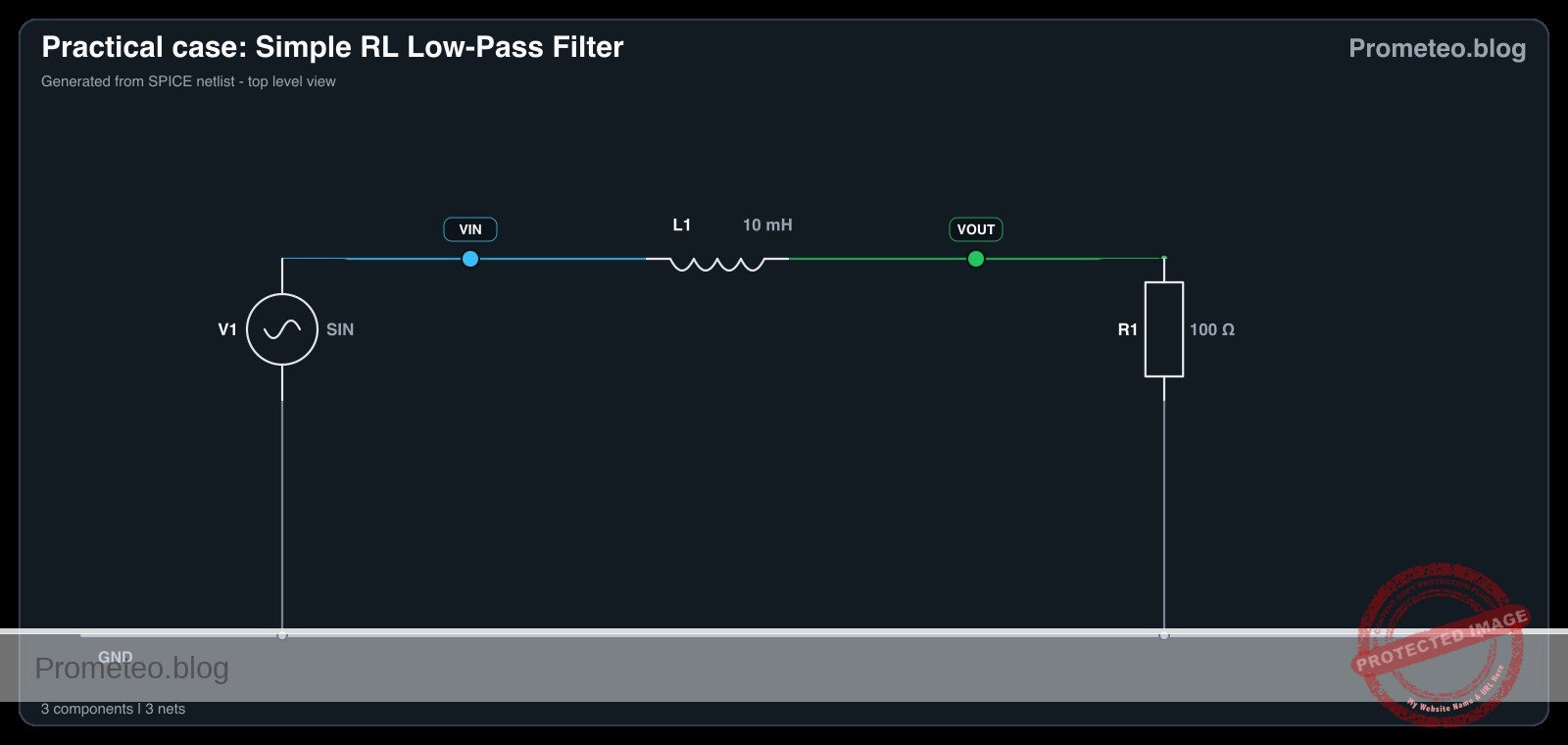
Practical case: Noise suppression with RF choke

Level: Medium – Demonstrate the high impedance of the inductor at high frequencies to block noise in power lines.

Objective and use case

You will construct an LR low-pass filter using an RF choke to isolate a DC power line from high-frequency AC noise. By superimposing an AC signal onto a DC voltage supply, you will observe how the inductor’s frequency-dependent reactance permits DC to pass while heavily attenuating high-frequency noise before it reaches the load.

This circuit concept is highly useful in the real world for:
* Preventing high-frequency switching noise from entering sensitive analog sensor circuits.
* Filtering out radio frequency interference (RFI) from long power supply lines.
* Isolating different functional blocks that share a common power rail on a PCB.
* Protecting automotive audio and communication electronics from alternator whine.

Expected outcome:
* The mixed input signal (V_IN_MIX) will display a steady DC offset combined with significant high-frequency ripples.
* The output voltage (V_OUT_CLEAN) across the load will show a stable DC level with the AC noise vastly reduced.
* An FFT (Fast Fourier Transform) analysis of the input will reveal a large 0 Hz (DC) component and a prominent high-frequency peak.
* An FFT analysis of the output will show the high-frequency peak almost completely suppressed, confirming the choke’s blocking action.

Target audience: Intermediate electronics students learning about reactive components and AC/DC superimposition.

Materials

  • V1: 5 V DC source, function: main DC power supply
  • V2: 500 mV peak sine wave AC source at 100 kHz, function: high-frequency noise simulator
  • L1: 1 mH inductor, function: RF choke to block high-frequency noise
  • R1: 100 Ω resistor, function: load simulation

Wiring guide

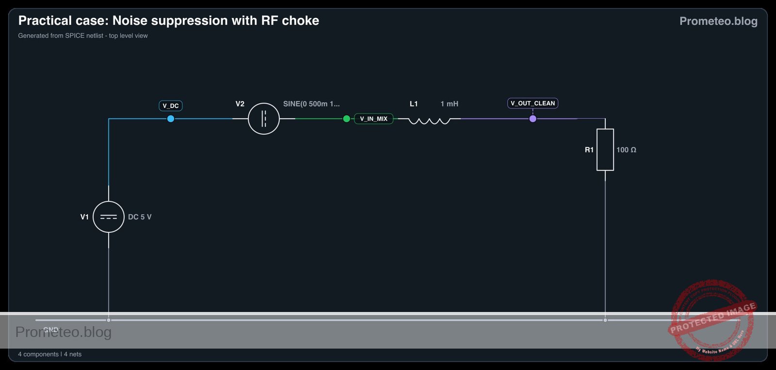
  • V1: connects between V_DC and 0
  • V2: connects between V_IN_MIX and V_DC
  • L1: connects between V_IN_MIX and V_OUT_CLEAN
  • R1: connects between V_OUT_CLEAN and 0

Conceptual block diagram
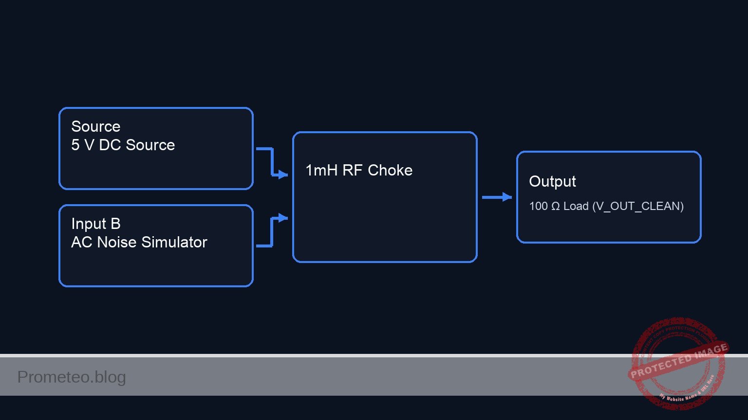
Conceptual block diagram — 1mH RF Choke
Quick read: inputs → main block → output (actuator or measurement). This summarizes the ASCII schematic below.

Schematic

[ V1: 5 V DC Source ] --(V_DC)--> [ V2: AC Noise Simulator ] --(V_IN_MIX)--> [ L1: 1mH RF Choke ] --(V_OUT_CLEAN)--> [ R1: 100 Ω Load ] --> GND
Electrical Schematic

Electrical diagram

Electrical diagram for case: Practical case: Noise suppression with RF choke
Generated from the validated SPICE netlist for this case.

🔒 This electrical diagram is premium. With the monthly membership (7-day free trial) you can unlock the complete didactic material and the print-ready PDF pack.🔓 See premium access plans

Measurements and tests

  1. Connect an oscilloscope probe to V_IN_MIX with the ground clip attached to node 0. Set the channel coupling to DC. You should observe a 5 V DC baseline with a 1 V peak-to-peak 100 kHz sine wave riding on top of it.
  2. Connect a second oscilloscope probe to V_OUT_CLEAN. Observe that the DC voltage remains at approximately 5 V, but the high-frequency 100 kHz ripple is drastically attenuated due to the high inductive reactance (XL = 2\pi fL) of the choke.
  3. Activate the FFT (Fast Fourier Transform) math function on the oscilloscope for the V_IN_MIX channel. Note the massive spike at 0 Hz (representing the 5 V DC component) and the distinct noise spike at 100 kHz.
  4. Apply the FFT function to the V_OUT_CLEAN channel. Compare the magnitude of the 100 kHz spike against the input measurement; it should be significantly reduced, successfully proving the inductor’s high-frequency blocking capabilities.

SPICE netlist and simulation

Reference SPICE Netlist (ngspice) — excerptFull SPICE netlist (ngspice)

* Noise suppression with RF choke
.width out=256

* Main DC power supply (5V)
V1 V_DC 0 DC 5

* High-frequency noise simulator (500mV peak, 100kHz sine wave superimposed on DC)
V2 V_IN_MIX V_DC SINE(0 500m 100k)

* RF choke to block high-frequency noise (1mH)
L1 V_IN_MIX V_OUT_CLEAN 1m

* Load simulation (100 ohms)
* ... (truncated in public view) ...

Copy this content into a .cir file and run with ngspice.

🔒 Part of this section is premium. With the monthly membership (7-day free trial) you can access the full content (materials, wiring, detailed build, validation, troubleshooting, variants and checklist) and download the complete print-ready PDF pack.

* Noise suppression with RF choke
.width out=256

* Main DC power supply (5V)
V1 V_DC 0 DC 5

* High-frequency noise simulator (500mV peak, 100kHz sine wave superimposed on DC)
V2 V_IN_MIX V_DC SINE(0 500m 100k)

* RF choke to block high-frequency noise (1mH)
L1 V_IN_MIX V_OUT_CLEAN 1m

* Load simulation (100 ohms)
R1 V_OUT_CLEAN 0 100

* Analysis directives
.op
* Simulate for 100us to capture 10 full cycles of the 100kHz noise
.tran 0.1u 100u
.print tran V(V_IN_MIX) V(V_OUT_CLEAN) V(V_DC) I(L1)

.end

Simulation Results (Transient Analysis)

Simulation Results (Transient Analysis)
Analysis: The simulation shows a 5V DC signal with a superimposed 500mV peak 100kHz sine wave at the input (V_IN_MIX ranges from 4.5V to 5.5V). At the output (V_OUT_CLEAN), the voltage ranges from 4.92V to 5.12V, indicating that the 1mH RF choke significantly attenuates the high-frequency noise while passing the DC component to the 100-ohm load.
Show raw data table (1008 rows)
Index   time            v(v_in_mix)     v(v_out_clean)  v(v_dc)         l1#branch
0	0.000000e+00	5.000000e+00	5.000000e+00	5.000000e+00	5.000000e-02
1	1.000000e-09	5.000314e+00	5.000000e+00	5.000000e+00	5.000000e-02
2	2.000000e-09	5.000628e+00	5.000000e+00	5.000000e+00	5.000000e-02
3	4.000000e-09	5.001257e+00	5.000000e+00	5.000000e+00	5.000000e-02
4	8.000000e-09	5.002513e+00	5.000001e+00	5.000000e+00	5.000001e-02
5	1.600000e-08	5.005026e+00	5.000004e+00	5.000000e+00	5.000004e-02
6	3.200000e-08	5.010052e+00	5.000016e+00	5.000000e+00	5.000016e-02
7	6.400000e-08	5.020101e+00	5.000064e+00	5.000000e+00	5.000064e-02
8	1.280000e-07	5.040169e+00	5.000256e+00	5.000000e+00	5.000256e-02
9	2.280000e-07	5.071384e+00	5.000808e+00	5.000000e+00	5.000808e-02
10	3.280000e-07	5.102316e+00	5.001665e+00	5.000000e+00	5.001665e-02
11	4.280000e-07	5.132845e+00	5.002818e+00	5.000000e+00	5.002818e-02
12	5.280000e-07	5.162850e+00	5.004261e+00	5.000000e+00	5.004261e-02
13	6.280000e-07	5.192212e+00	5.005985e+00	5.000000e+00	5.005985e-02
14	7.280000e-07	5.220816e+00	5.007980e+00	5.000000e+00	5.007980e-02
15	8.280000e-07	5.248548e+00	5.010236e+00	5.000000e+00	5.010236e-02
16	9.280000e-07	5.275299e+00	5.012741e+00	5.000000e+00	5.012741e-02
17	1.028000e-06	5.300963e+00	5.015481e+00	5.000000e+00	5.015481e-02
18	1.128000e-06	5.325440e+00	5.018443e+00	5.000000e+00	5.018443e-02
19	1.228000e-06	5.348633e+00	5.021613e+00	5.000000e+00	5.021613e-02
20	1.328000e-06	5.370449e+00	5.024976e+00	5.000000e+00	5.024976e-02
21	1.428000e-06	5.390804e+00	5.028515e+00	5.000000e+00	5.028515e-02
22	1.528000e-06	5.409616e+00	5.032213e+00	5.000000e+00	5.032213e-02
23	1.628000e-06	5.426812e+00	5.036054e+00	5.000000e+00	5.036054e-02
... (984 more rows) ...


Reference SPICE netlist (ngspice)

* Noise suppression with RF choke
.width out=256

* Main DC power supply (5V)
V1 V_DC 0 DC 5

* High-frequency noise simulator (500mV peak, 100kHz sine wave superimposed on DC)
V2 V_IN_MIX V_DC SINE(0 500m 100k)

* RF choke to block high-frequency noise (1mH)
L1 V_IN_MIX V_OUT_CLEAN 1m

* Load simulation (100 ohms)
R1 V_OUT_CLEAN 0 100

* Analysis directives
.op
* Simulate for 100us to capture 10 full cycles of the 100kHz noise
.tran 0.1u 100u
.print tran V(V_IN_MIX) V(V_OUT_CLEAN) V(V_DC) I(L1)

.end

Simulation Results (Transient Analysis)

Simulation Results (Transient Analysis)
Analysis: The simulation shows a 5V DC signal with a superimposed 500mV peak 100kHz sine wave at the input (V_IN_MIX ranges from 4.5V to 5.5V). At the output (V_OUT_CLEAN), the voltage ranges from 4.92V to 5.12V, indicating that the 1mH RF choke significantly attenuates the high-frequency noise while passing the DC component to the 100-ohm load.

Common mistakes and how to avoid them

  • Using an inductor with a low self-resonant frequency (SRF): All inductors have parasitic winding capacitance. If the noise frequency exceeds the inductor’s SRF, the component behaves like a capacitor and allows high-frequency noise to pass straight through. Always verify the SRF is well above your target noise frequency.
  • Neglecting the inductor’s DC resistance (DCR): Inductors are made of coiled wire which naturally possesses resistance. High load currents passing through an inductor with high DCR will cause an unacceptable DC voltage drop. Choose a choke with an appropriately low DCR for your load.
  • Core saturation due to high DC current: If the load draws more continuous current than the inductor’s saturation rating (Isat), the core’s magnetic flux saturates. This causes the inductance to drop sharply, destroying its filtering capability. Always check the saturation current rating.

Troubleshooting

  • Symptom: High-frequency noise is still heavily present at V_OUT_CLEAN.
  • Cause: The inductor value is too low to provide significant reactance at the simulated noise frequency, or its SRF has been exceeded.
  • Fix: Increase the inductance value (e.g., scale from 10 µH to 1 mH) or verify the frequency limits of the specific choke being used.
  • Symptom: Significant DC voltage drop at V_OUT_CLEAN under load (e.g., reading 4 V instead of 5 V).
  • Cause: The inductor’s internal DC resistance (DCR) is too high relative to the load resistor R1.
  • Fix: Replace the inductor with a physically larger one that uses thicker wire, which lowers the DCR, or increase the load resistance if it’s drawing more current than intended.
  • Symptom: The choke gets excessively hot during operation.
  • Cause: The DC current drawn by the load exceeds the continuous thermal current rating (Irms) of the inductor.
  • Fix: Select a higher-rated power inductor capable of safely handling the steady-state load current.

Possible improvements and extensions

  • Form an LC Low-Pass Filter: Add a decoupling capacitor (e.g., 100 nF or 1 µF) parallel to the load (between V_OUT_CLEAN and 0). This creates a second-order filter, providing a much steeper roll-off and vastly superior noise attenuation compared to the simple LR configuration.
  • Implement a Pi-Filter: Use a Capacitor-Inductor-Capacitor (C-L-C) arrangement to provide bidirectional noise suppression. This not only cleans the power entering the load but also prevents any switching noise generated by the load from polluting the main DC supply line.

More Practical Cases on Prometeo.blog

Find this product and/or books on this topic on Amazon

Go to Amazon

As an Amazon Associate, I earn from qualifying purchases. If you buy through this link, you help keep this project running.

Quick Quiz

Question 1: What is the primary purpose of the inductor in the described circuit?


Question 2: What type of filter is constructed in this experiment?


Question 3: How does the inductor react to the DC portion of the signal?


Question 4: Which of the following is a real-world application of this circuit concept mentioned in the text?


Question 5: What will the mixed input signal (V_IN_MIX) display according to the expected outcomes?


Question 6: Based on the expected outcomes, what is the effect of the circuit on the output voltage (V_OUT_CLEAN)?


Question 7: What is the stated difficulty level of demonstrating the high impedance of the inductor in this context?


Question 8: What specific type of interference can this circuit filter out from long power supply lines?


Question 9: How does the circuit help different functional blocks that share a common power rail on a PCB?


Question 10: What component is specifically used as an RF choke in this low-pass filter circuit?


Carlos Núñez Zorrilla
Electronics & Computer Engineer

Telecommunications Electronics Engineer and Computer Engineer (official degrees in Spain).
Follow me:


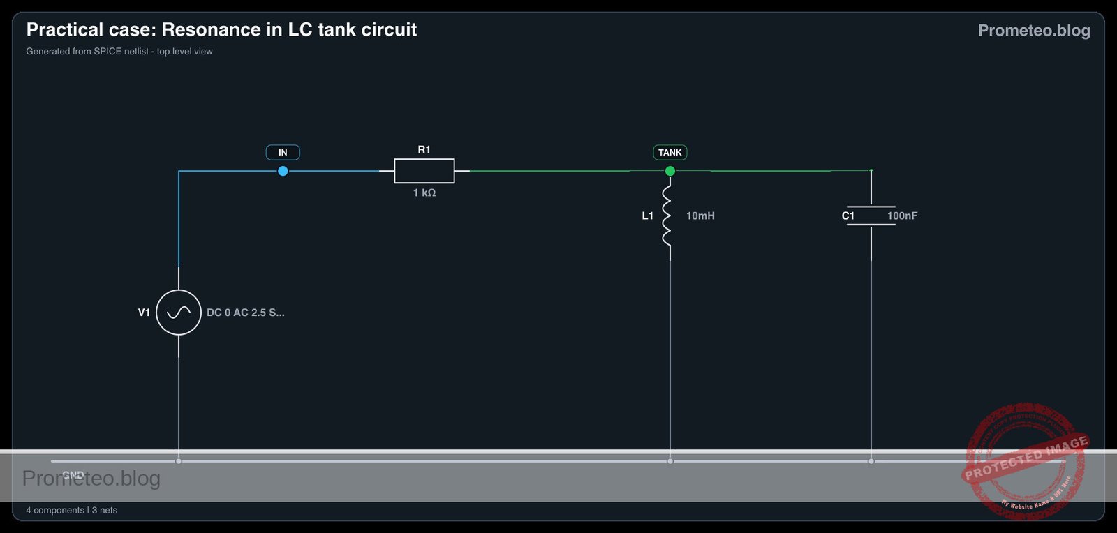
Practical case: Resonance in LC tank circuit

Level: Medium | Analyze the energy exchange and determine the resonant frequency of an AC-driven LC tank.

Objective and use case

In this practical case, you will build a parallel LC tank circuit driven by an AC sine wave source through a series resistor. By sweeping the input frequency, you will observe the precise point where inductive and capacitive reactances cancel out, maximizing the circuit’s impedance.

Understanding LC resonance is essential in modern electronics because these circuits are the fundamental building blocks of frequency selection. Real-world applications include:
* Radio frequency (RF) tuning: Selecting a specific station’s frequency while rejecting others.
* Audio and signal filtering: Creating band-pass or band-stop (notch) filters to eliminate noise.
* Wireless power transfer: Maximizing the efficiency of inductive coupling between transmitter and receiver coils.
* Oscillator circuits: Generating stable clock signals for microcontrollers and transceivers.

Expected outcome:
* You will calculate the theoretical resonant frequency based on the chosen $L$ and $C$ values.
* The total current drawn from the source (Itotal) will drop to its minimum value at resonance.
* The voltage across the LC tank (VLC) will peak at the resonant frequency.
* You will observe how energy continuously sloshes back and forth between the capacitor’s electric field and the inductor’s magnetic field.

Target audience: Intermediate electronics students transitioning from DC basics to AC reactive circuits.

Materials

  • V1: 5 V peak-to-peak AC voltage source, function: sine wave generator for frequency sweep
  • R1: 1 kΩ resistor, function: source impedance to allow voltage variations across the tank
  • L1: 10 mH inductor, function: magnetic energy storage
  • C1: 100 nF ceramic or film capacitor, function: electric energy storage

Wiring guide

  • V1: Connect the positive terminal to node IN and the negative terminal to node 0 (GND).
  • R1: Connect one pin to node IN and the other pin to node TANK.
  • L1: Connect one pin to node TANK and the other pin to node 0 (GND).
  • C1: Connect one pin to node TANK and the other pin to node 0 (GND).

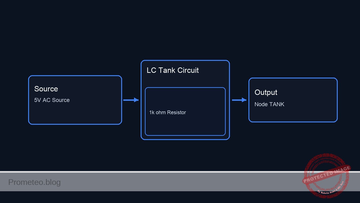
Conceptual block diagram

Conceptual block diagram — LC Tank Circuit
Quick read: inputs → main block → output (actuator or measurement). This summarizes the ASCII schematic below.

Schematic

[ V1: 5 V AC ] --(IN)--> [ R1: 1k ohm ] --(Node TANK)--+--> [ L1: 10mH ] --> GND
                                                      |
                                                      +--> [ C1: 100nF ] --> GND
Electrical Schematic

Electrical diagram

Electrical diagram for case: Practical case: Resonance in LC tank circuit
Generated from the validated SPICE netlist for this case.

🔒 This electrical diagram is premium. With the monthly membership (7-day free trial) you can unlock the complete didactic material and the print-ready PDF pack.🔓 See premium access plans

Measurements and tests

  1. Calculate the theoretical resonant frequency (fr):
    Use the formula fr = (1 / 2\pi\sqrtLC). With L = 10 mH and C = 100 nF, the expected resonant frequency is approximately 5032 Hz.
  2. Set up the frequency sweep:
    Configure V1 to output a 5 V peak-to-peak sine wave. Begin with a frequency of 1 kHz and gradually increase it up to 10 kHz.
  3. Measure VLC (Tank Voltage):
    Monitor the voltage amplitude at node TANK relative to node 0 (GND) using an oscilloscope or an AC voltmeter. As you approach 5 kHz, the voltage amplitude will rise steadily, hitting a sharp maximum exactly at resonance, and then fall as the frequency increases further.
  4. Measure Itotal (Source Current):
    Measure the current flowing through R1 (this can be done by observing the voltage difference between IN and TANK and applying Ohm’s law: Itotal = ((VIN – VTANK) / R1)). Note that at resonance, the parallel LC tank exhibits maximum impedance, meaning Itotal will drop to its minimum.
  5. Calculate the circuit’s Q-factor:
    Identify the -3dB (half-power) frequencies above and below the resonance peak to find the bandwidth ($BW$). The Quality Factor is Q = (fr / BW).

SPICE netlist and simulation

Reference SPICE Netlist (ngspice) — excerptFull SPICE netlist (ngspice)

* Practical case: Resonance in LC tank circuit
.width out=256

* 5V peak-to-peak implies an amplitude of 2.5V. 
* The resonant frequency of 10mH and 100nF is approximately 5033 Hz.
* We configure V1 with both a transient sine wave at resonance and an AC magnitude for optional AC analysis.
V1 IN 0 DC 0 AC 2.5 SIN(0 2.5 5033)

* Source impedance
R1 IN TANK 1k

* LC Tank circuit components
L1 TANK 0 10mH
* ... (truncated in public view) ...

Copy this content into a .cir file and run with ngspice.

🔒 Part of this section is premium. With the monthly membership (7-day free trial) you can access the full content (materials, wiring, detailed build, validation, troubleshooting, variants and checklist) and download the complete print-ready PDF pack.

* Practical case: Resonance in LC tank circuit
.width out=256

* 5V peak-to-peak implies an amplitude of 2.5V. 
* The resonant frequency of 10mH and 100nF is approximately 5033 Hz.
* We configure V1 with both a transient sine wave at resonance and an AC magnitude for optional AC analysis.
V1 IN 0 DC 0 AC 2.5 SIN(0 2.5 5033)

* Source impedance
R1 IN TANK 1k

* LC Tank circuit components
L1 TANK 0 10mH
C1 TANK 0 100nF

* Operating point and Transient analysis
.op
.tran 1u 2m

* Print directives for logging the input and output (resonance) nodes
.print tran V(IN) V(TANK) I(L1)

.end

Simulation Results (Transient Analysis)

Simulation Results (Transient Analysis)
Analysis: The transient simulation shows the input voltage V(IN) oscillating as a sine wave with a 2.5V amplitude (5V peak-to-peak). The voltage at the tank node V(TANK) closely follows V(IN) with nearly the same amplitude, and the inductor current oscillates, confirming the resonant behavior of the LC tank circuit at the specified frequency.
Show raw data table (2015 rows)
Index   time            v(in)           v(tank)         l1#branch
0	0.000000e+00	0.000000e+00	0.000000e+00	0.000000e+00
1	1.000000e-08	7.905818e-04	7.905026e-08	7.905026e-14
2	1.084006e-08	8.569951e-04	8.624878e-08	8.629565e-14
3	1.252017e-08	9.898217e-04	1.017615e-07	1.020896e-13
4	1.588039e-08	1.255475e-03	1.394809e-07	1.426210e-13
5	2.260084e-08	1.786781e-03	2.416948e-07	2.707046e-13
6	3.604174e-08	2.849394e-03	5.532131e-07	8.049184e-13
7	5.708432e-08	4.512980e-03	1.327631e-06	2.783809e-12
8	8.603868e-08	6.802053e-03	2.965106e-06	8.998482e-12
9	1.305078e-07	1.031768e-02	6.769425e-06	3.064276e-11
10	1.955195e-07	1.545732e-02	1.514065e-05	1.018634e-10
11	2.946313e-07	2.329267e-02	3.431881e-05	3.469641e-10
12	4.417944e-07	3.492633e-02	7.707420e-05	1.166612e-09
13	6.644501e-07	5.252635e-02	1.741480e-04	3.963414e-09
14	9.972436e-07	7.882720e-02	3.917455e-04	1.337970e-08
15	1.499113e-06	1.184727e-01	8.834917e-04	4.537981e-08
16	2.252017e-06	1.778899e-01	1.987598e-03	1.534626e-07
17	3.252017e-06	2.566456e-01	4.126641e-03	4.591745e-07
18	4.252017e-06	3.351447e-01	7.022468e-03	1.016630e-06
19	5.252017e-06	4.133086e-01	1.066173e-02	1.900840e-06
20	6.252017e-06	4.910592e-01	1.502968e-02	3.185410e-06
21	7.252017e-06	5.683189e-01	2.011023e-02	4.942405e-06
22	8.252017e-06	6.450102e-01	2.588597e-02	7.242215e-06
23	9.252017e-06	7.210565e-01	3.233820e-02	1.015342e-05
... (1991 more rows) ...


Reference SPICE netlist (ngspice)

* Practical case: Resonance in LC tank circuit
.width out=256

* 5V peak-to-peak implies an amplitude of 2.5V.
* The resonant frequency of 10mH and 100nF is approximately 5033 Hz.
* We configure V1 with both a transient sine wave at resonance and an AC magnitude for optional AC analysis.
V1 IN 0 DC 0 AC 2.5 SIN(0 2.5 5033)

* Source impedance
R1 IN TANK 1k

* LC Tank circuit components
L1 TANK 0 10mH
C1 TANK 0 100nF

* Operating point and Transient analysis
.op
.tran 1u 2m

* Print directives for logging the input and output (resonance) nodes
.print tran V(IN) V(TANK) I(L1)

.end

Simulation Results (Transient Analysis)

Simulation Results (Transient Analysis)
Analysis: The transient simulation shows the input voltage V(IN) oscillating as a sine wave with a 2.5V amplitude (5V peak-to-peak). The voltage at the tank node V(TANK) closely follows V(IN) with nearly the same amplitude, and the inductor current oscillates, confirming the resonant behavior of the LC tank circuit at the specified frequency.

Common mistakes and how to avoid them

  • Using a polarized capacitor in an AC circuit: Electrolytic capacitors are generally polarized and can fail or explode if subjected to reversing AC voltages. Always use non-polarized capacitors (like ceramic or film) for an LC tank.
  • Ignoring the inductor’s Equivalent Series Resistance (ESR): Real inductors consist of long coils of wire, adding parasitic DC resistance to the tank. If the measured Q-factor is much lower than expected (resulting in a wider, flatter peak), inductor ESR is usually the culprit.
  • Confusing angular frequency (\omega) with standard frequency ($f$): Remember that \omega = (1 / \sqrtLC) yields results in radians per second. You must divide by 2\pi to get the frequency in Hertz.

Troubleshooting

  • Symptom: The measured resonant frequency is significantly higher or lower than the calculated 5032 Hz.
    • Cause: Component tolerances. Standard ceramic capacitors can have a ±20% tolerance, and inductors often have ±10%.
    • Fix: Measure the exact values of L1 and C1 using an LCR meter and recalculate the expected frequency.
  • Symptom: VLC shows no noticeable peak during the sweep; the voltage remains relatively flat.
    • Cause: The chosen frequency sweep range does not cover the resonant point, or R1 is too small, effectively shorting the tank to the rigid voltage source.
    • Fix: Double-check the math for your specific $L$ and $C$ values to ensure the sweep range encompasses fr. Ensure R1 is adequately sized (1 kΩ is a good starting point).
  • Symptom: Signal distortion or clipping is observed at node TANK.
    • Cause: The AC source might be overdriving the circuit, or core saturation is occurring in the inductor (if using a very small ferrite core at high currents).
    • Fix: Reduce the amplitude of V1 from 5 V to 1 V peak-to-peak and check if the sine wave becomes clean again.

Possible improvements and extensions

  • Vary the damping resistor: Swap R1 for different values (e.g., 470 Ω, 10 kΩ) or add a resistor directly in parallel with the LC tank. Observe and chart how this affects the sharpness of the resonance peak (the Q-factor).
  • Build an active oscillator: Remove the AC source and connect the LC tank to a transistor or an op-amp with positive feedback (such as a Colpitts or Hartley configuration) to create a standalone circuit that generates its own continuous sine wave at the resonant frequency.

More Practical Cases on Prometeo.blog

Find this product and/or books on this topic on Amazon

Go to Amazon

As an Amazon Associate, I earn from qualifying purchases. If you buy through this link, you help keep this project running.

Quick Quiz

Question 1: What is the primary objective of sweeping the input frequency in the described LC tank circuit?


Question 2: In a parallel LC tank circuit at resonance, what happens to the total current drawn from the source?


Question 3: What happens to the voltage across the LC tank at the resonant frequency?


Question 4: How does energy behave in an LC tank circuit at resonance?


Question 5: Which of the following is a real-world application of LC resonance mentioned in the text?


Question 6: What is the function of the series resistor (R1) in this practical case?


Question 7: What type of source is used to drive the LC tank circuit in this practical case?


Question 8: In the context of audio and signal filtering, what can LC circuits be used to create?


Question 9: Why is understanding LC resonance essential for wireless power transfer?


Question 10: Who is the target audience for this practical case?


Carlos Núñez Zorrilla
Electronics & Computer Engineer

Telecommunications Electronics Engineer and Computer Engineer (official degrees in Spain).
Follow me:


Practical case: Boost converter storage

Level: Medium | Understand magnetic energy storage to boost voltage.

Objective and use case

In this practical case, you will build a basic open-loop Boost converter to demonstrate how an inductor stores and releases magnetic energy to step up a DC voltage.

Why it is useful:
* Allows battery-powered devices to operate at higher voltages (e.g., generating 5 V from a single 3.7 V Li-ion cell).
* Drives strings of LEDs that require a constant, high forward voltage.
* Captures and steps up voltage in energy harvesting and regenerative braking systems.
* Provides versatile power rails in compact portable electronics without requiring multiple batteries.

Expected outcome:
* You will observe the inductor current (I_inductor) ramping up when the switch is closed and ramping down when it opens.
* The output voltage (V_out) will be demonstrably higher than the input voltage source.
* You will record the direct relationship between the switch’s Duty Cycle and the resulting V_out magnitude.

Target audience and level:
Intermediate electronics students learning the fundamentals of switch-mode power supplies.

Materials

  • V1: 5 V DC source, function: main power input
  • V2: Pulse voltage source (0-5 V, 100kHz, 50% duty cycle), function: PWM signal for the switch
  • L1: 100 µH inductor, function: magnetic energy storage
  • M1: N-channel MOSFET (e.g., IRLZ44N), function: main switching element
  • D1: Schottky diode (e.g., 1N5819), function: prevents reverse current from capacitor
  • C1: 47 µF capacitor, function: output voltage smoothing
  • R1: 100 Ω resistor, function: basic load to discharge capacitor

Wiring guide

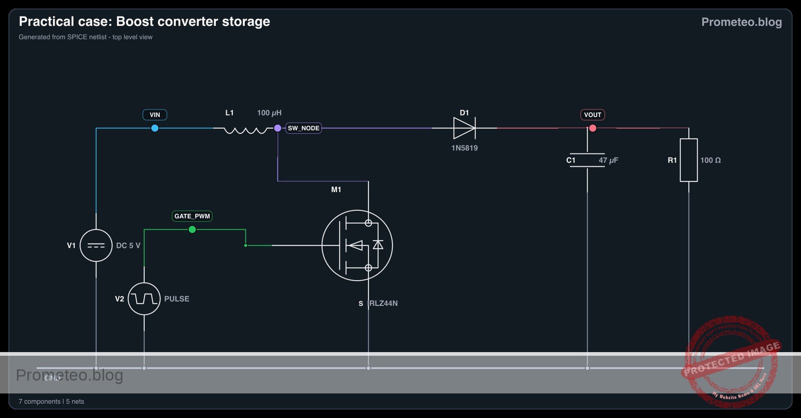
  • V1: connects between VIN and 0 (GND).
  • V2: connects between GATE_PWM and 0 (GND).
  • L1: connects between VIN and SW_NODE.
  • M1: Drain connects to SW_NODE, Gate connects to GATE_PWM, Source connects to 0 (GND).
  • D1: Anode connects to SW_NODE, Cathode connects to VOUT.
  • C1: connects between VOUT and 0 (GND).
  • R1: connects between VOUT and 0 (GND).

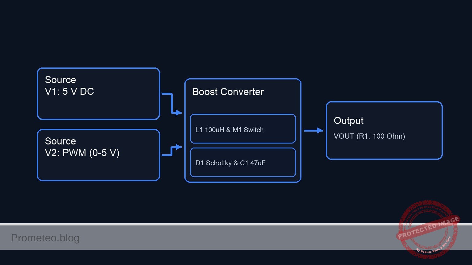
Conceptual block diagram

Conceptual block diagram — Boost Converter
Quick read: inputs → main block → output (actuator or measurement). This summarizes the ASCII schematic below.

Schematic

Control Signal:
[ V2: PWM (0-5 V) ] --(GATE_PWM)--> [ M1:Gate ]

Power & Switching Path:
[ V1: 5 V DC ] --(VIN)--> [ L1: 100µH ] --(SW_NODE)--> [ M1:Drain ] --(Switch)--> [ M1:Source ] --> GND
                                             |
Boost Output & Load:                         |
                                             +--> [ D1: Schottky ] --(VOUT)--> [ R1: 100 Ω ] --> GND
                                                                       |
                                                                       +--> [ C1: 47µF ] --> GND
Electrical Schematic

Electrical diagram

Electrical diagram for case: Practical case: Boost converter storage
Generated from the validated SPICE netlist for this case.

🔒 This electrical diagram is premium. With the monthly membership (7-day free trial) you can unlock the complete didactic material and the print-ready PDF pack.🔓 See premium access plans

Measurements and tests

  1. Initial state check: Apply V1 (5 V) with V2 turned off (0% duty cycle). Measure VOUT. The voltage should be roughly 4.7 V (the 5 V input minus the forward voltage drop of the Schottky diode).
  2. Switching activation: Activate V2 to supply a 100kHz square wave at a 50% duty cycle. Measure VOUT across R1. The voltage should rise to approximately 9 V-10 V, demonstrating the step-up action.
  3. Inductor current observation: Probe the current flowing through L1 (I_inductor). You will observe a triangular waveform. The upward slope occurs while M1 is ON (energy storage), and the downward slope occurs while M1 is OFF (energy release to VOUT).
  4. Duty Cycle mapping: Adjust the Duty Cycle of V2 from 30% to 70% in 10% increments. Record VOUT at each step to verify that a higher duty cycle yields a higher output voltage.

SPICE netlist and simulation

Reference SPICE Netlist (ngspice) — excerptFull SPICE netlist (ngspice)

* Boost converter storage

* Main power input
V1 VIN 0 DC 5

* PWM signal for the switch (100kHz, 50% duty cycle)
V2 GATE_PWM 0 PULSE(0 5 0 10n 10n 5u 10u)

* Magnetic energy storage
L1 VIN SW_NODE 100u

* Main switching element (N-channel MOSFET)
* Drain: SW_NODE, Gate: GATE_PWM, Source: 0, Bulk: 0
M1 SW_NODE GATE_PWM 0 0 IRLZ44N

* Prevents reverse current from capacitor
* Anode: SW_NODE, Cathode: VOUT
D1 SW_NODE VOUT 1N5819

* Output voltage smoothing
* ... (truncated in public view) ...

Copy this content into a .cir file and run with ngspice.

🔒 Part of this section is premium. With the monthly membership (7-day free trial) you can access the full content (materials, wiring, detailed build, validation, troubleshooting, variants and checklist) and download the complete print-ready PDF pack.

* Boost converter storage

* Main power input
V1 VIN 0 DC 5

* PWM signal for the switch (100kHz, 50% duty cycle)
V2 GATE_PWM 0 PULSE(0 5 0 10n 10n 5u 10u)

* Magnetic energy storage
L1 VIN SW_NODE 100u

* Main switching element (N-channel MOSFET)
* Drain: SW_NODE, Gate: GATE_PWM, Source: 0, Bulk: 0
M1 SW_NODE GATE_PWM 0 0 IRLZ44N

* Prevents reverse current from capacitor
* Anode: SW_NODE, Cathode: VOUT
D1 SW_NODE VOUT 1N5819

* Output voltage smoothing
C1 VOUT 0 47u

* Basic load to discharge capacitor
R1 VOUT 0 100

* Models
.model IRLZ44N NMOS(Level=1 VTO=2.0 KP=10.0 RS=0.05 RD=0.05)
.model 1N5819 D(IS=1e-6 RS=0.1 N=1.05 EG=0.69 XTI=2)

* Output Directives
* VOUT is the main output, GATE_PWM is the input stimulus
.print tran V(VOUT) V(GATE_PWM) V(SW_NODE) V(VIN) I(L1)

* Analysis
* Time constant is R*C = 4.7ms. Simulating for 10ms to observe steady-state boost voltage.
.op
.tran 0.1u 10m

.end

Simulation Results (Transient Analysis)

Simulation Results (Transient Analysis)
Analysis: The simulation shows the boost converter operating correctly. The output voltage (VOUT) starts near 5V and rises to a steady-state value of approximately 9.6V, with the switch node (SW_NODE) switching between ~0V and ~10V as driven by the 100kHz PWM signal.
Show raw data table (119800 rows)
Index   time            v(vout)         v(gate_pwm)     v(sw_node)      v(vin)          l1#branch
0	0.000000e+00	4.702912e+00	0.000000e+00	5.000000e+00	5.000000e+00	4.702912e-02
1	1.000000e-10	4.702912e+00	5.000000e-02	4.999798e+00	5.000000e+00	4.702912e-02
2	2.000000e-10	4.702912e+00	1.000000e-01	4.999798e+00	5.000000e+00	4.702912e-02
3	4.000000e-10	4.702912e+00	2.000000e-01	4.999797e+00	5.000000e+00	4.702912e-02
4	8.000000e-10	4.702912e+00	4.000000e-01	4.999797e+00	5.000000e+00	4.702912e-02
5	1.600000e-09	4.702912e+00	8.000000e-01	4.999797e+00	5.000000e+00	4.702912e-02
6	3.200000e-09	4.702912e+00	1.600000e+00	4.999797e+00	5.000000e+00	4.702913e-02
7	6.400000e-09	4.702910e+00	3.200000e+00	8.651034e-03	5.000000e+00	4.710899e-02
8	1.000000e-08	4.702907e+00	5.000000e+00	6.306948e-03	5.000000e+00	4.728872e-02
9	1.064000e-08	4.702906e+00	5.000000e+00	6.311218e-03	5.000000e+00	4.732068e-02
10	1.192000e-08	4.702905e+00	5.000000e+00	6.319746e-03	5.000000e+00	4.738460e-02
11	1.448000e-08	4.702902e+00	5.000000e+00	6.336800e-03	5.000000e+00	4.751244e-02
12	1.960000e-08	4.702897e+00	5.000000e+00	6.370908e-03	5.000000e+00	4.776811e-02
13	2.984000e-08	4.702887e+00	5.000000e+00	6.439123e-03	5.000000e+00	4.827946e-02
14	5.032000e-08	4.702866e+00	5.000000e+00	6.575553e-03	5.000000e+00	4.930212e-02
15	9.128000e-08	4.702825e+00	5.000000e+00	6.848406e-03	5.000000e+00	5.134738e-02
16	1.732000e-07	4.702743e+00	5.000000e+00	7.394086e-03	5.000000e+00	5.543754e-02
17	2.732000e-07	4.702643e+00	5.000000e+00	8.060152e-03	5.000000e+00	6.042981e-02
18	3.732000e-07	4.702543e+00	5.000000e+00	8.726166e-03	5.000000e+00	6.542142e-02
19	4.732000e-07	4.702443e+00	5.000000e+00	9.392128e-03	5.000000e+00	7.041236e-02
20	5.732000e-07	4.702343e+00	5.000000e+00	1.005804e-02	5.000000e+00	7.540264e-02
21	6.732000e-07	4.702243e+00	5.000000e+00	1.072390e-02	5.000000e+00	8.039225e-02
22	7.732000e-07	4.702143e+00	5.000000e+00	1.138970e-02	5.000000e+00	8.538119e-02
23	8.732000e-07	4.702043e+00	5.000000e+00	1.205546e-02	5.000000e+00	9.036947e-02
... (119776 more rows) ...


Reference SPICE netlist (ngspice)

* Boost converter storage

* Main power input
V1 VIN 0 DC 5

* PWM signal for the switch (100kHz, 50% duty cycle)
V2 GATE_PWM 0 PULSE(0 5 0 10n 10n 5u 10u)

* Magnetic energy storage
L1 VIN SW_NODE 100u

* Main switching element (N-channel MOSFET)
* Drain: SW_NODE, Gate: GATE_PWM, Source: 0, Bulk: 0
M1 SW_NODE GATE_PWM 0 0 IRLZ44N

* Prevents reverse current from capacitor
* Anode: SW_NODE, Cathode: VOUT
D1 SW_NODE VOUT 1N5819

* Output voltage smoothing
C1 VOUT 0 47u

* Basic load to discharge capacitor
R1 VOUT 0 100

* Models
.model IRLZ44N NMOS(Level=1 VTO=2.0 KP=10.0 RS=0.05 RD=0.05)
.model 1N5819 D(IS=1e-6 RS=0.1 N=1.05 EG=0.69 XTI=2)

* Output Directives
* VOUT is the main output, GATE_PWM is the input stimulus
.print tran V(VOUT) V(GATE_PWM) V(SW_NODE) V(VIN) I(L1)

* Analysis
* Time constant is R*C = 4.7ms. Simulating for 10ms to observe steady-state boost voltage.
.op
.tran 0.1u 10m

.end

Simulation Results (Transient Analysis)

Simulation Results (Transient Analysis)
Analysis: The simulation shows the boost converter operating correctly. The output voltage (VOUT) starts near 5V and rises to a steady-state value of approximately 9.6V, with the switch node (SW_NODE) switching between ~0V and ~10V as driven by the 100kHz PWM signal.

Common mistakes and how to avoid them

  • Using a standard rectifier diode (e.g., 1N4007): Standard diodes are too slow to turn off at 100kHz, leading to massive switching losses and poor voltage conversion. Always use a fast-recovery or Schottky diode like the 1N5819.
  • Inductor core saturation: If the inductor’s maximum current rating is lower than the peak switching current, the magnetic core will saturate. The inductor will then act as a short circuit, potentially destroying the MOSFET. Always verify the inductor’s saturation current rating.
  • Operating without a load: Running a boost converter with no load resistor (R1) can cause the output voltage to continuously rise with every switching cycle, theoretically reaching infinity and destroying the output capacitor or MOSFET. Always include a minimum load.

Troubleshooting

  • Symptom: Output voltage equals the input voltage (minus diode drop).
  • Cause: The MOSFET is not switching. V2 might be disconnected or the voltage level is too low to surpass the MOSFET’s gate threshold.
  • Fix: Check the GATE_PWM signal with an oscilloscope. Use a logic-level MOSFET if your PWM signal is limited to 3.3 V or 5 V.
  • Symptom: MOSFET becomes extremely hot very quickly.
  • Cause: The inductor is saturating, or the MOSFET has a high ON-resistance (RDS(on)) and is experiencing high conduction losses.
  • Fix: Swap the inductor for one with a higher current rating. Ensure the gate drive voltage is sufficient to turn the MOSFET completely ON.
  • Symptom: Unstable or highly rippled output voltage.
  • Cause: The output capacitor C1 is too small for the load or has a high Equivalent Series Resistance (ESR).
  • Fix: Increase the capacitance of C1 or place a ceramic capacitor in parallel with the electrolytic capacitor to lower the overall ESR.

Possible improvements and extensions

  • Closed-loop control: Add a voltage divider at the output connected to an error amplifier or microcontroller analog input. Dynamically adjust the PWM duty cycle to maintain a constant VOUT regardless of changes in R1 (the load).
  • Synchronous rectification: Replace the Schottky diode D1 with a second P-channel or driven N-channel MOSFET. Switching this second MOSFET synchronously (inversely to M1) reduces the voltage drop typical of a diode, significantly improving overall converter efficiency.

More Practical Cases on Prometeo.blog

Find this product and/or books on this topic on Amazon

Go to Amazon

As an Amazon Associate, I earn from qualifying purchases. If you buy through this link, you help keep this project running.

Quick Quiz

Question 1: What is the primary purpose of the Boost converter in this practical case?


Question 2: Which component is responsible for storing and releasing magnetic energy?


Question 3: What happens to the inductor current when the switch is closed?


Question 4: Which of the following is a mentioned use case for a Boost converter?


Question 5: What happens to the inductor current when the switch opens?


Question 6: What parameter of the switch has a direct relationship with the magnitude of the output voltage?


Question 7: How can a Boost converter benefit battery-powered devices?


Question 8: What role does the Boost converter play in energy harvesting systems?


Question 9: What is the expected relationship between the output voltage and the input voltage source?


Question 10: Who is the target audience for this practical case?


Carlos Núñez Zorrilla
Electronics & Computer Engineer

Telecommunications Electronics Engineer and Computer Engineer (official degrees in Spain).

Follow me:


Practical case: Inductive peak protection

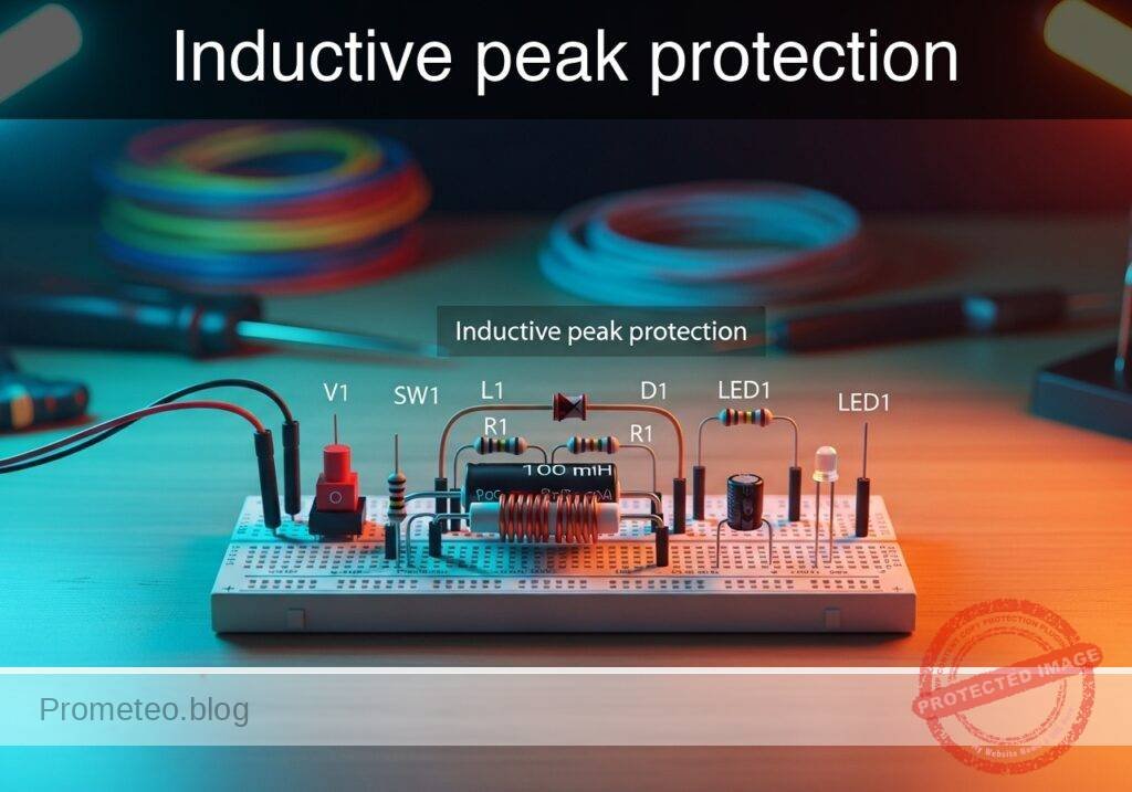
Inductive peak protection prototype (Maker Style)

Level: Medium | Objective: Analyze the transient voltage generated when disconnecting an inductor and mitigate it using a flyback diode.

Objective and use case

In this practical case, you will build a switched inductor circuit monitored by an oscilloscope to observe the destructive voltage spike (inductive kickback) that occurs when current is abruptly interrupted. You will then install a flyback diode in parallel with the inductive load to safely clamp this transient voltage.

Why it is useful:
* Prevents catastrophic overvoltage damage to sensitive switching components such as transistors, MOSFETs, and microcontroller pins.
* Significantly reduces electromagnetic interference (EMI) and radio frequency interference (RFI) caused by high-voltage arcing across mechanical switch contacts.
* Increases the reliability, safety, and lifespan of power supply systems, motor controllers, and relay-driven circuits.

Expected outcome:
* Without the diode, opening the switch will produce a massive negative voltage spike on the oscilloscope, often reaching hundreds of volts.
* With the flyback diode installed, the transient spike will be immediately clamped to a safe level of approximately -0.7 V.
* The stored magnetic energy will safely dissipate as a steadily decaying circulating current through the inductor-resistor-diode loop.

Target audience and level: Intermediate electronics students learning about reactive components, energy storage, and circuit protection techniques.

Materials

  • V1: 12 V DC supply, function: main power source
  • SW1: SPST toggle or push-button switch, function: circuit connection control
  • L1: 100 mH inductor, function: magnetic energy storage
  • R1: 100 Ω resistor, function: limits steady-state current to 120 mA
  • D1: 1N4007 rectifier diode, function: flyback protection

Wiring guide

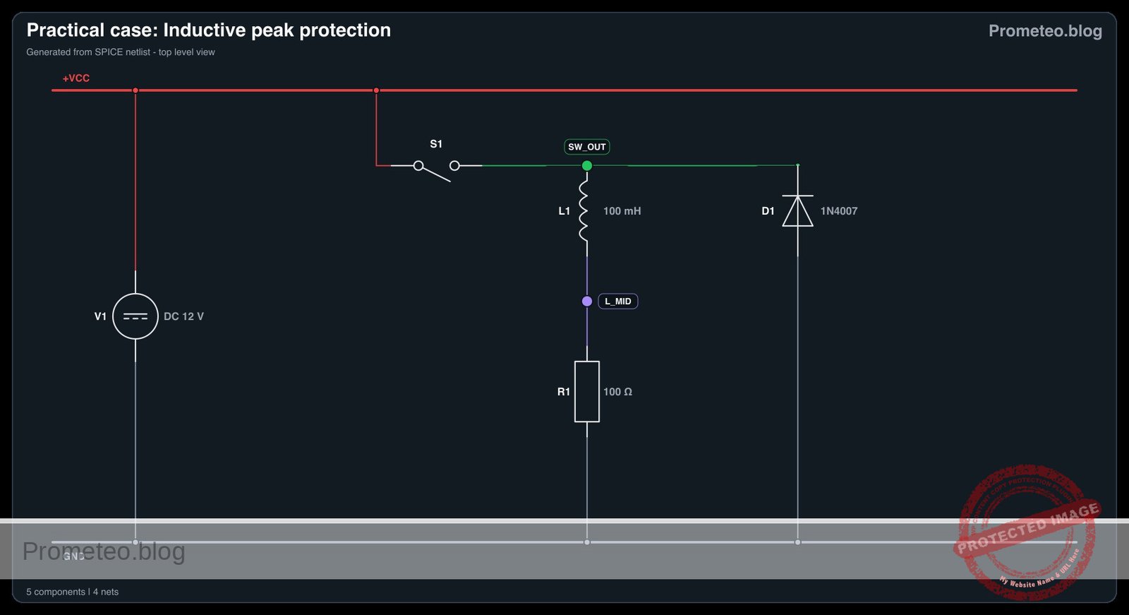
  • V1: connects between node VCC (positive) and node 0 (ground).
  • SW1: connects between node VCC and node SW_OUT.
  • L1: connects between node SW_OUT and node L_MID.
  • R1: connects between node L_MID and node 0.
  • D1: connects between node 0 (Anode) and node SW_OUT (Cathode) for reverse bias during normal closed-switch operation.

Conceptual block diagram

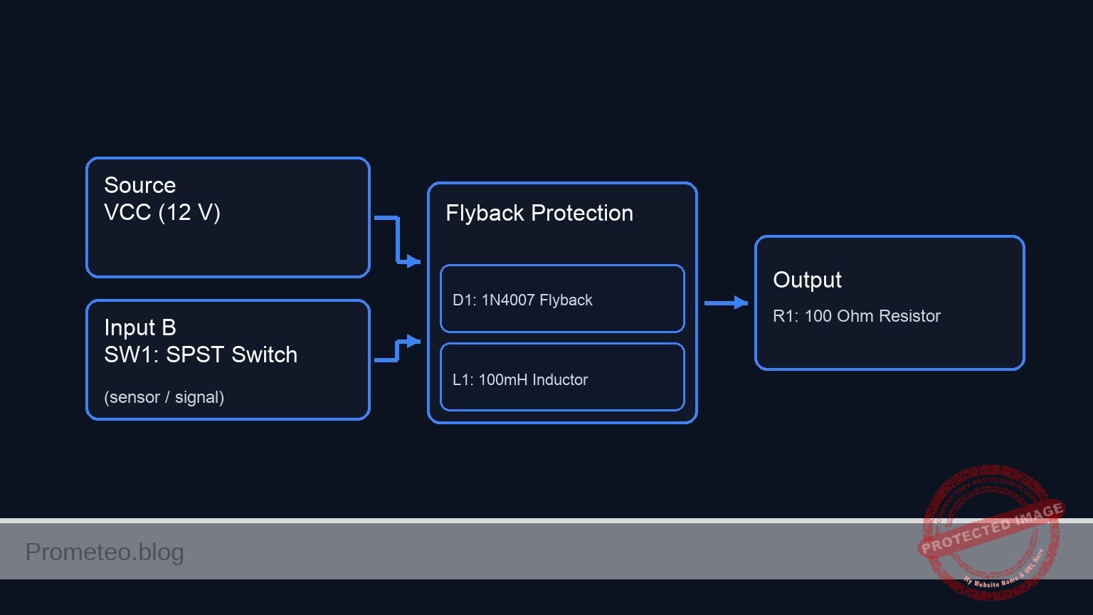
Conceptual block diagram — Flyback Protection
Quick read: inputs → main block → output (actuator or measurement). This summarizes the ASCII schematic below.

Schematic

VCC (12 V) --> [ SW1: SPST Switch ] --(SW_OUT)--> [ L1: 100mH Inductor ] --(L_MID)--> [ R1: 100 Ω Resistor ] --> GND
                                         ^
                                         |
                              (Cathode)  |
                           [ D1: 1N4007 Flyback ]
                              (Anode)    ^
                                         |
                                        GND
Electrical Schematic

Electrical diagram

Electrical diagram for case: Inductive peak protection
Generated from the validated SPICE netlist for this case.

🔒 This electrical diagram is premium. With the monthly membership (7-day free trial) you can unlock the complete didactic material and the print-ready PDF pack.🔓 See premium access plans

Measurements and tests

  1. Connect the oscilloscope probe to node SW_OUT and attach the ground clip to node 0. Set the oscilloscope trigger to a falling edge, single-shot mode.
  2. Begin with the flyback diode (D1) completely disconnected from the circuit.
  3. Close the switch (SW1) to allow current to flow. Wait a moment for the magnetic field in the inductor to fully build up.
  4. Quickly open the switch (SW1). Observe the oscilloscope capture; you will see a massive negative voltage transient as the inductor acts as a current source, forcing current across the open switch gap.
  5. Connect the flyback diode (D1), verifying that the cathode (striped end) connects to node SW_OUT and the anode connects to node 0.
  6. Repeat the switching process. The oscilloscope trace will now show the negative transient safely clamped at roughly -0.7 V as the diode forward-biases to provide a safe discharge path.

SPICE netlist and simulation

Reference SPICE Netlist (ngspice) — excerptFull SPICE netlist (ngspice)

* Inductive peak protection
.width out=256

V1 VCC 0 DC 12

* SW1 modeled as a voltage-controlled switch connecting VCC to SW_OUT
S1 VCC SW_OUT SW_CTRL 0 SW_MODEL
V_SW_CTRL SW_CTRL 0 PULSE(0 5 100u 1u 1u 500u 1000u)
.model SW_MODEL SW(VT=2.5 VH=0.1 RON=0.01 ROFF=100Meg)

L1 SW_OUT L_MID 100m
R1 L_MID 0 100

* ... (truncated in public view) ...

Copy this content into a .cir file and run with ngspice.

🔒 Part of this section is premium. With the monthly membership (7-day free trial) you can access the full content (materials, wiring, detailed build, validation, troubleshooting, variants and checklist) and download the complete print-ready PDF pack.

* Inductive peak protection
.width out=256

V1 VCC 0 DC 12

* SW1 modeled as a voltage-controlled switch connecting VCC to SW_OUT
S1 VCC SW_OUT SW_CTRL 0 SW_MODEL
V_SW_CTRL SW_CTRL 0 PULSE(0 5 100u 1u 1u 500u 1000u)
.model SW_MODEL SW(VT=2.5 VH=0.1 RON=0.01 ROFF=100Meg)

L1 SW_OUT L_MID 100m
R1 L_MID 0 100

* Flyback protection diode
D1 0 SW_OUT 1N4007
.model 1N4007 D(IS=1e-9 N=1.9 RS=0.03 BV=1000 IBV=5e-08 CJO=10p VJ=0.7 M=0.5 TT=1e-07)

.op
.tran 1u 2000u
.print tran V(SW_CTRL) V(SW_OUT) V(L_MID) V(VCC) I(L1)

.end

Simulation Results (Transient Analysis)

Simulation Results (Transient Analysis)
Analysis: The transient analysis spans 0 s to 2 ms and captures the switching interval. The switching node and inductor current remain bounded, consistent with the flyback path protecting the switch. Main ranges: l1#branch 120 nA -> 62.7 mA; v(sw_out) -884 mV -> 12 V; v(l_mid) 12 uV -> 6.27 V.
Show raw data table (2088 rows)
Index   time            v(sw_ctrl)      v(sw_out)       v(l_mid)        v(vcc)          l1#branch
0	0.000000e+00	0.000000e+00	1.199996e-05	1.199996e-05	1.200000e+01	1.199996e-07
1	1.000000e-08	0.000000e+00	1.199996e-05	1.199996e-05	1.200000e+01	1.199996e-07
2	2.000000e-08	0.000000e+00	1.199996e-05	1.199996e-05	1.200000e+01	1.199996e-07
3	4.000000e-08	0.000000e+00	1.199996e-05	1.199996e-05	1.200000e+01	1.199996e-07
4	8.000000e-08	0.000000e+00	1.199996e-05	1.199996e-05	1.200000e+01	1.199996e-07
5	1.600000e-07	0.000000e+00	1.199996e-05	1.199996e-05	1.200000e+01	1.199996e-07
6	3.200000e-07	0.000000e+00	1.199996e-05	1.199996e-05	1.200000e+01	1.199996e-07
7	6.400000e-07	0.000000e+00	1.199996e-05	1.199996e-05	1.200000e+01	1.199996e-07
8	1.280000e-06	0.000000e+00	1.199996e-05	1.199996e-05	1.200000e+01	1.199996e-07
9	2.280000e-06	0.000000e+00	1.199996e-05	1.199996e-05	1.200000e+01	1.199996e-07
10	3.280000e-06	0.000000e+00	1.199996e-05	1.199996e-05	1.200000e+01	1.199996e-07
11	4.280000e-06	0.000000e+00	1.199996e-05	1.199996e-05	1.200000e+01	1.199996e-07
12	5.280000e-06	0.000000e+00	1.199996e-05	1.199996e-05	1.200000e+01	1.199996e-07
13	6.280000e-06	0.000000e+00	1.199996e-05	1.199996e-05	1.200000e+01	1.199996e-07
14	7.280000e-06	0.000000e+00	1.199996e-05	1.199996e-05	1.200000e+01	1.199996e-07
15	8.280000e-06	0.000000e+00	1.199996e-05	1.199996e-05	1.200000e+01	1.199996e-07
16	9.280000e-06	0.000000e+00	1.199996e-05	1.199996e-05	1.200000e+01	1.199996e-07
17	1.028000e-05	0.000000e+00	1.199996e-05	1.199996e-05	1.200000e+01	1.199996e-07
18	1.128000e-05	0.000000e+00	1.199996e-05	1.199996e-05	1.200000e+01	1.199996e-07
19	1.228000e-05	0.000000e+00	1.199996e-05	1.199996e-05	1.200000e+01	1.199996e-07
20	1.328000e-05	0.000000e+00	1.199996e-05	1.199996e-05	1.200000e+01	1.199996e-07
21	1.428000e-05	0.000000e+00	1.199996e-05	1.199996e-05	1.200000e+01	1.199996e-07
22	1.528000e-05	0.000000e+00	1.199996e-05	1.199996e-05	1.200000e+01	1.199996e-07
23	1.628000e-05	0.000000e+00	1.199996e-05	1.199996e-05	1.200000e+01	1.199996e-07
... (2064 more rows) ...


Reference SPICE netlist (ngspice)

* Inductive peak protection
.width out=256

V1 VCC 0 DC 12

* SW1 modeled as a voltage-controlled switch connecting VCC to SW_OUT
S1 VCC SW_OUT SW_CTRL 0 SW_MODEL
V_SW_CTRL SW_CTRL 0 PULSE(0 5 100u 1u 1u 500u 1000u)
.model SW_MODEL SW(VT=2.5 VH=0.1 RON=0.01 ROFF=100Meg)

L1 SW_OUT L_MID 100m
R1 L_MID 0 100

* Flyback protection diode
D1 0 SW_OUT 1N4007
.model 1N4007 D(IS=1e-9 N=1.9 RS=0.03 BV=1000 IBV=5e-08 CJO=10p VJ=0.7 M=0.5 TT=1e-07)

.op
.tran 1u 2000u
.print tran V(SW_CTRL) V(SW_OUT) V(L_MID) V(VCC) I(L1)

.end

Simulation Results (Transient Analysis)

Simulation Results (Transient Analysis)
Analysis: The transient analysis spans 0 s to 2 ms and captures the switching interval. The switching node and inductor current remain bounded, consistent with the flyback path protecting the switch. Main ranges: l1#branch 120 nA -> 62.7 mA; v(sw_out) -884 mV -> 12 V; v(l_mid) 12 uV -> 6.27 V.

Common mistakes and how to avoid them

  • Reversing the diode polarity: Placing the diode with the anode pointing to the positive voltage node creates a direct short circuit to ground when the switch is closed. This will destroy the diode or trigger the power supply’s overcurrent protection. Always ensure the cathode faces the higher potential.
  • Using a diode with inadequate current rating: The flyback diode must safely handle a peak forward current equal to the steady-state current of the inductor just before switching. Always use properly rated rectifier, Schottky, or fast-recovery diodes.
  • Omitting the series resistor: Connecting a pure inductor directly across a high-current DC source acts as a near short-circuit once the magnetic field is fully established. Always include a current-limiting series resistor, or ensure the inductor (such as a relay coil) has sufficient internal DC resistance.

Troubleshooting

  • Symptom: The power supply shuts down or its current limit LED turns on immediately upon closing the switch.
    • Cause: The flyback diode is installed backwards, creating a short circuit from the power source to ground.
    • Fix: Disconnect power immediately and flip the diode so its striped end (cathode) faces the switch node.
  • Symptom: A massive voltage spike still appears on the oscilloscope even with the diode supposedly installed.
    • Cause: The diode may have blown open due to a previous overcurrent event, or the breadboard connection is loose.
    • Fix: Verify diode continuity using a multimeter’s diode mode, and check the physical seating of the pins at the switch and ground nodes.
  • Symptom: The oscilloscope trace shows high-frequency ringing instead of a clean clamp.
    • Cause: Parasitic capacitance in the switch, wiring, or oscilloscope probes interacting with the inductor.
    • Fix: Ensure the oscilloscope probe is properly compensated (x10 mode recommended for high voltage spikes) and keep ground leads as short as physically possible.

Possible improvements and extensions

  • Automated switching with a MOSFET: Replace the mechanical switch with an N-channel MOSFET driven by a square wave generator (configured as a low-side switch) to observe repetitive clamping on the oscilloscope in real-time.
  • Fast discharge using a Zener diode: Add an appropriately rated Zener diode in series with the standard flyback diode (anode connected to anode). This allows the inductor to discharge its energy much faster by clamping the voltage at a higher, but strictly controlled, level.

More Practical Cases on Prometeo.blog

Find this product and/or books on this topic on Amazon

Go to Amazon

As an Amazon Associate, I earn from qualifying purchases. If you buy through this link, you help keep this project running.

Quick Quiz

Question 1: What is the main purpose of the flyback diode in this inductive load circuit?


Question 2: Which component stores energy in its magnetic field while current is flowing?


Question 3: What happens to the inductor current immediately after the switch opens?


Question 4: Why can an unprotected inductive load damage a switching device?


Question 5: In the SPICE model, what does the pulsed switch-control source represent?


Question 6: During normal energized operation, what should the flyback diode ideally do?


Question 7: Which measurement is most useful to observe the switching transient in the simulation?


Question 8: What role does R1 play in this practical model?


Question 9: Why is this circuit relevant for relays, solenoids and small motors?


Question 10: What should a correct validation show for this case before publication?


Carlos Núñez Zorrilla
Electronics & Computer Engineer

Telecommunications Electronics Engineer and Computer Engineer (official degrees in Spain).
Follow me:


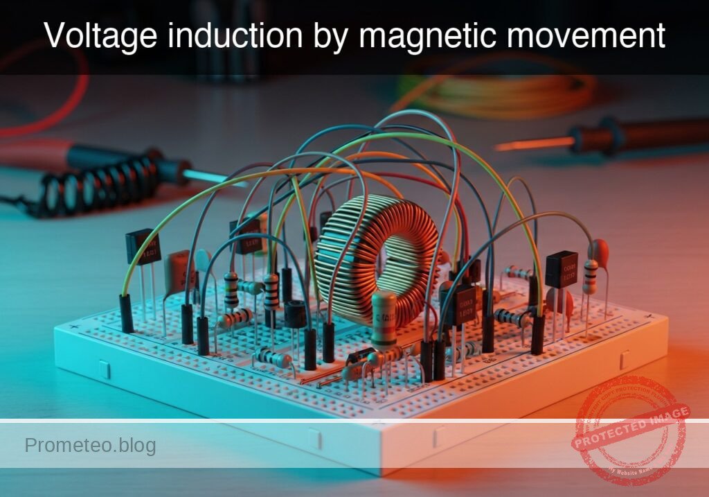
Practical case: Voltage induction by magnetic movement

Voltage induction by magnetic movement prototype (Maker Style)

Level: Basic. Demonstrate how moving a magnet through a coil generates an electromotive force (EMF).

Objective and use case

In this practical case, you will construct a fundamental electromagnetic induction demonstrator using a hand-wound copper coil and a high-strength neodymium magnet. You will observe how kinetic energy is converted into electrical energy via Faraday’s Law of Induction.

Why it is useful:
* Power Generation: This mechanism illustrates the core principle behind electric generators, alternators, and wind turbines.
* Audio Technology: This is the operating principle for dynamic microphones and electric guitar pickups (transducers).
* Sensors: Used in automotive ABS speed sensors and industrial position sensors.
* Wireless Charging: Demonstrates the basics of magnetic coupling used in phone chargers.

Expected outcome:
* A measurable voltage spike (positive or negative) on the multimeter when the magnet moves relative to the coil.
* The LED flashes briefly when the magnet is moved rapidly, indicating a voltage peak exceeding the diode’s forward voltage (~1.8 V).
* Reversing the direction of the magnet’s movement reverses the polarity of the induced voltage.

Target audience: Students and hobbyists introducing themselves to Faraday’s Law and passive components.

Materials

  • L1: Air core coil (approx. 500–1000 turns of enameled copper wire), function: induction element.
  • MAG1: Cylindrical Neodymium magnet (fit to pass inside L1), function: source of magnetic flux.
  • D1: Red LED, function: indicator for positive phase induction.
  • D2: Green LED, function: indicator for negative phase induction (connected in anti-parallel).
  • M1: Multimeter (set to 200 mV or 2 V DC range), function: voltage monitor.

Wiring guide

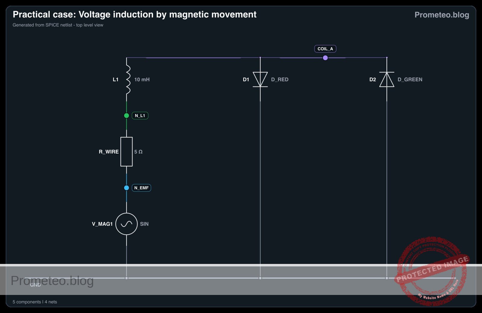
The circuit consists of the coil connected directly to the indicators in parallel. We define the coil terminals as nodes COIL_A and COIL_B.

  • L1: Connects between node COIL_A and node COIL_B.
  • D1: Anode connects to COIL_A; Cathode connects to COIL_B.
  • D2: Anode connects to COIL_B; Cathode connects to COIL_A (anti-parallel to D1).
  • M1: Positive probe connects to COIL_A; Negative probe connects to COIL_B.

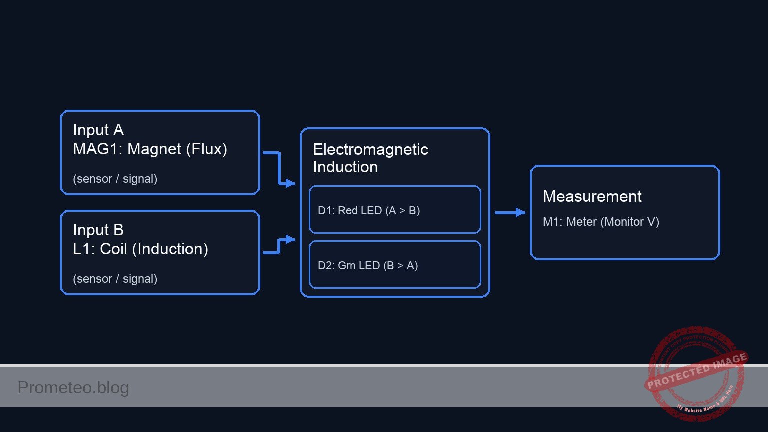
Conceptual block diagram

Conceptual block diagram — Electromagnetic Induction
Quick read: inputs → main block → output (actuator or measurement). This summarizes the ASCII schematic below.

Schematic

markdown
Title: Practical case: Voltage induction by magnetic movement

[ INPUT / SOURCE ]                       [ DISTRIBUTION RAILS ]                    [ OUTPUT / LOADS ]

                                                 (Node A: Top Rail)
                                    /------------------------------------------------------------------>
                                    |                |                    |                    |
[ MAG1: Magnet ] --(Flux)--> [ L1: Coil ]            | (Anode)            | (Cathode)          | (+)
                                    |                v                    v                    v
                                    |        [ D1: Red LED ]      [ D2: Grn LED ]      [ M1: Meter ]
                                    |        (Lights if A > B)    (Lights if B > A)    (Monitor V)
                                    |                |                    |                    |
                                    |                | (Cathode)          | (Anode)            | (-)
                                    \                v                    v                    v
                                    \------------------------------------------------------------------>
                                                 (Node B: Bottom Rail)
Schematic (ASCII)

Electrical diagram

Electrical diagram for case: Voltage induction by magnetic movement
Generated from the validated SPICE netlist for this case.

🔒 This electrical diagram is premium. With the monthly membership (7-day free trial) you can unlock the complete didactic material and the print-ready PDF pack.🔓 See premium access plans

Measurements and tests

  1. Static Test: Place the magnet inside the coil and hold it completely still. The multimeter should read 0 V, and no LEDs should light up. This confirms that a changing magnetic field is required.
  2. Slow Insertion: Set the multimeter to the lowest DC voltage range (e.g., 200 mV). Slowly push the magnet into the coil. Observe a small voltage reading (e.g., +10 to +50 mV).
  3. Fast Action: Quickly thrust the magnet into the coil. You should see a significantly higher voltage spike (potentially > 1 V) and D1 (Red) may flash briefly.
  4. Reverse Motion: Quickly pull the magnet out of the coil. The voltage polarity on the multimeter will flip (negative sign), and D2 (Green) should flash.
  5. Oscillation: Move the magnet back and forth rapidly inside the coil. The LEDs should flicker alternately, demonstrating the generation of Alternating Current (AC).

SPICE netlist and simulation

Reference SPICE Netlist (ngspice) — excerptFull SPICE netlist (ngspice)

* Practical case: Voltage induction by magnetic movement
.width out=256
*
* Description:
* Simulation of a magnet moving through a coil, inducing voltage to drive two antiparallel LEDs.
*
* Nodes:
* COIL_A : Hot terminal of the coil (Multimeter +)
* COIL_B : Reference terminal of the coil (Multimeter -, Grounded)
*
* Note: The physical "Coil" is modeled as a series combination of an EMF Voltage Source (V_MAG1),
* a Resistor (R_WIRE), and the Inductor (L1).

* --- Power / Reference ---
* Grounding COIL_B as per Multimeter negative probe convention
V_REF COIL_B 0 0

* --- Magnetic Induction Source (MAG1) ---
* Simulating the changing magnetic flux from MAG1 as an AC voltage source.
* 3V Peak, 5Hz (Simulates shaking the magnet)
* ... (truncated in public view) ...

Copy this content into a .cir file and run with ngspice.

🔒 Part of this section is premium. With the monthly membership (7-day free trial) you can access the full content (materials, wiring, detailed build, validation, troubleshooting, variants and checklist) and download the complete print-ready PDF pack.

* Practical case: Voltage induction by magnetic movement
.width out=256
*
* Description:
* Simulation of a magnet moving through a coil, inducing voltage to drive two antiparallel LEDs.
*
* Nodes:
* COIL_A : Hot terminal of the coil (Multimeter +)
* COIL_B : Reference terminal of the coil (Multimeter -, Grounded)
*
* Note: The physical "Coil" is modeled as a series combination of an EMF Voltage Source (V_MAG1),
* a Resistor (R_WIRE), and the Inductor (L1).

* --- Power / Reference ---
* Grounding COIL_B as per Multimeter negative probe convention
V_REF COIL_B 0 0

* --- Magnetic Induction Source (MAG1) ---
* Simulating the changing magnetic flux from MAG1 as an AC voltage source.
* 3V Peak, 5Hz (Simulates shaking the magnet)
V_MAG1 N_EMF COIL_B SIN(0 3 5)

* --- Coil Assembly (L1) ---
* Internal wire resistance
R_WIRE N_EMF N_L1 5
* The physical inductance L1
L1 N_L1 COIL_A 10m

* --- Indicators ---
* D1: Red LED (Indicates Positive Phase)
* Anode: COIL_A, Cathode: COIL_B
D1 COIL_A COIL_B D_RED

* D2: Green LED (Indicates Negative Phase)
* Anode: COIL_B, Cathode: COIL_A
D2 COIL_B COIL_A D_GREEN

* --- Multimeter (M1) ---
* Modeled as the voltage difference V(COIL_A) - V(COIL_B)
* (Implicit in the node voltages)

* --- Models ---
* Generic LED Models
.model D_RED D(IS=1e-18 N=2 RS=10 BV=5)
.model D_GREEN D(IS=1e-18 N=2.5 RS=10 BV=5)

* --- Simulation Directives ---
.op
* Transient analysis: 1ms step, 500ms duration (2.5 cycles at 5Hz)
.tran 1m 500m

* --- Output ---
* Monitoring the induced voltage at COIL_A
.print tran V(COIL_A) I(L1)

Simulation Results (Transient Analysis)

Simulation Results (Transient Analysis)

Analysis: The transient analysis shows an AC voltage at COIL_A oscillating between approx +2.6V and -2.8V at 5Hz. Current flows through L1, peaking around 66mA. The voltage levels are sufficient to forward bias the LEDs (D_RED and D_GREEN) alternately, consistent with the intended indication of positive and negative phases.
Show raw data table (522 rows)
Index   time            v(coil_a)       l1#branch
0	0.000000e+00	4.375392e-35	-8.75078e-36
1	1.000000e-05	9.424778e-04	1.884985e-15
2	2.000000e-05	1.884955e-03	3.769970e-15
3	4.000000e-05	3.769910e-03	7.539938e-15
4	8.000000e-05	7.539814e-03	1.507987e-14
5	1.600000e-04	1.507958e-02	3.015936e-14
6	3.200000e-04	3.015878e-02	6.031856e-14
7	6.400000e-04	6.031451e-02	1.206316e-13
8	1.280000e-03	1.206046e-01	2.412214e-13
9	2.280000e-03	2.147012e-01	4.294658e-13
10	3.280000e-03	3.085859e-01	6.175653e-13
11	4.280000e-03	4.021661e-01	8.067202e-13
12	5.280000e-03	4.953494e-01	1.005111e-12
13	6.280000e-03	5.880438e-01	1.262566e-12
14	7.280000e-03	6.801579e-01	1.873422e-12
15	8.280000e-03	7.716008e-01	4.548512e-12
16	9.280000e-03	8.622822e-01	1.907006e-11
17	1.028000e-02	9.521126e-01	1.003825e-10
18	1.128000e-02	1.041003e+00	5.511221e-10
19	1.228000e-02	1.128867e+00	3.003086e-09
20	1.328000e-02	1.215616e+00	1.605415e-08
21	1.428000e-02	1.301164e+00	8.389370e-08
22	1.528000e-02	1.385424e+00	4.276266e-07
23	1.628000e-02	1.468291e+00	2.121308e-06
... (498 more rows) ...


Reference SPICE netlist (ngspice)

* Practical case: Voltage induction by magnetic movement
.width out=256
*
* Description:
* Simulation of a magnet moving through a coil, inducing voltage to drive two antiparallel LEDs.
*
* Nodes:
* COIL_A : Hot terminal of the coil (Multimeter +)
* COIL_B : Reference terminal of the coil (Multimeter -, Grounded)
*
* Note: The physical "Coil" is modeled as a series combination of an EMF Voltage Source (V_MAG1),
* a Resistor (R_WIRE), and the Inductor (L1).

* --- Power / Reference ---
* Grounding COIL_B as per Multimeter negative probe convention
V_REF COIL_B 0 0

* --- Magnetic Induction Source (MAG1) ---
* Simulating the changing magnetic flux from MAG1 as an AC voltage source.
* 3V Peak, 5Hz (Simulates shaking the magnet)
V_MAG1 N_EMF COIL_B SIN(0 3 5)

* --- Coil Assembly (L1) ---
* Internal wire resistance
R_WIRE N_EMF N_L1 5
* The physical inductance L1
L1 N_L1 COIL_A 10m

* --- Indicators ---
* D1: Red LED (Indicates Positive Phase)
* Anode: COIL_A, Cathode: COIL_B
D1 COIL_A COIL_B D_RED

* D2: Green LED (Indicates Negative Phase)
* Anode: COIL_B, Cathode: COIL_A
D2 COIL_B COIL_A D_GREEN

* --- Multimeter (M1) ---
* Modeled as the voltage difference V(COIL_A) - V(COIL_B)
* (Implicit in the node voltages)

* --- Models ---
* Generic LED Models
.model D_RED D(IS=1e-18 N=2 RS=10 BV=5)
.model D_GREEN D(IS=1e-18 N=2.5 RS=10 BV=5)

* --- Simulation Directives ---
.op
* Transient analysis: 1ms step, 500ms duration (2.5 cycles at 5Hz)
.tran 1m 500m

* --- Output ---
* Monitoring the induced voltage at COIL_A
.print tran V(COIL_A) I(L1)

Simulation Results (Transient Analysis)

Simulation Results (Transient Analysis)

Analysis: The transient analysis shows an AC voltage at COIL_A oscillating between approx +2.6V and -2.8V at 5Hz. Current flows through L1, peaking around 66mA. The voltage levels are sufficient to forward bias the LEDs (D_RED and D_GREEN) alternately, consistent with the intended indication of positive and negative phases.

Common mistakes and how to avoid them

  1. Using weak magnets: Standard black ferrite magnets are often too weak to generate visible voltage on an LED. Solution: Use rare-earth Neodymium magnets.
  2. Moving too slowly: Faraday’s Law (V = – N · d\Phi / dt) depends on the rate of change. Solution: Move the magnet as quickly as possible to maximize the voltage spike.
  3. Insulation issues: Enameled wire has a clear coating that blocks electricity. Solution: Ensure the ends of the coil wire are sanded or scraped down to bare copper before connecting to the LEDs or multimeter.

Troubleshooting

  • Symptom: Multimeter shows voltage, but LEDs never light up.
    • Cause: The induced voltage is lower than the LED forward voltage threshold (~1.8 V).
    • Fix: Add more turns to the coil (increase $N$) or move the magnet faster.
  • Symptom: No reading on the multimeter even with fast movement.
    • Cause: Open circuit or poor connection at the coil tips.
    • Fix: Check continuity (resistance mode) across the coil terminals; it should read a few Ohms, not infinite.
  • Symptom: Voltage reading is erratic or hard to see.
    • Cause: Digital multimeters have a slow sample rate.
    • Fix: Use the «Max/Min» hold function if available, or use an analog (needle) multimeter which responds better to transient pulses.

Possible improvements and extensions

  1. Shake Flashlight: Add a bridge rectifier (4 diodes) and a large capacitor (e.g., 1000 µF) to store the energy generated by shaking the magnet, allowing the LED to stay lit for a few seconds after motion stops.
  2. Core Comparison: Insert an iron bolt inside the coil (making it an iron-core inductor) and move a magnet near the head of the bolt to observe how the ferromagnetic core concentrates the magnetic flux and affects induction.

More Practical Cases on Prometeo.blog

Find this product and/or books on this topic on Amazon

Go to Amazon

As an Amazon Associate, I earn from qualifying purchases. If you buy through this link, you help keep this project running.

Quick Quiz

Question 1: What core physical law does this practical case demonstrate?


Question 2: Which type of energy conversion takes place in this experiment?


Question 3: What component serves as the source of magnetic flux in this setup?


Question 4: Which real-world device operates on the same principle demonstrated here?


Question 5: What is the function of the LED in the circuit?


Question 6: What happens to the induced voltage polarity when the direction of the magnet's movement is reversed?


Question 7: To see the LED flash, the induced voltage peak must exceed approximately what value?


Question 8: What is the expected outcome on the multimeter when the magnet moves relative to the coil?


Question 9: Besides power generation, which automotive application uses this sensor technology?


Question 10: Which modern convenience technology is mentioned as using the basics of magnetic coupling?


Carlos Núñez Zorrilla
Electronics & Computer Engineer

Telecommunications Electronics Engineer and Computer Engineer (official degrees in Spain).
Follow me:


Practical case: Simple RL Low-Pass Filter

Simple RL Low-Pass Filter prototype (Maker Style)

Level: Basic – Observe how an inductor filters high frequencies in an RL series circuit.

Objective and use case

In this practical exercise, you will build a passive RL low-pass filter using a series inductor and a shunt resistor. This circuit demonstrates the inductive reactance property, where impedance increases with frequency, effectively blocking high-frequency signals while allowing low-frequency signals to pass through to the output.

Why it is useful:
* Audio Electronics: Used in crossover networks to direct low frequencies (bass) to woofers while blocking treble.
* Power Supplies: Essential for smoothing output currents and reducing ripple in DC/DC converters.
* Noise Suppression: Filters out high-frequency interference (EMI) on signal lines.
* Signal Conditioning: Removes high-frequency noise from sensor data before processing.

Expected outcome:
* Low Frequency Input (< Cutoff): The output amplitude (VOUT) is approximately equal to the input amplitude (VIN).
* Cutoff Frequency (fc): The output amplitude drops to roughly 70.7% of the input amplitude (-3dB point).
* High Frequency Input (> Cutoff): The output amplitude is significantly attenuated (reduced).
* Target audience: Basic electronics students and hobbyists exploring AC circuit theory.

Materials

  • V1: Function Generator (Sine wave source), function: AC signal injection
  • L1: 10 mH inductor, function: series reactive element (impedance increases with frequency)
  • R1: 100 Ω resistor, function: load/shunt resistor (output taken here)
  • Scope: Dual-channel Oscilloscope, function: visual comparison of Input vs. Output

Wiring guide

Construct the circuit using the following node connections. The output voltage is measured across the resistor.

  • V1 (Signal Source): Connects between node VIN (Positive) and node 0 (GND).
  • L1: Connects between node VIN and node VOUT.
  • R1: Connects between node VOUT and node 0 (GND).
  • Oscilloscope Channel 1: Connect probe tip to VIN and ground clip to 0.
  • Oscilloscope Channel 2: Connect probe tip to VOUT and ground clip to 0.

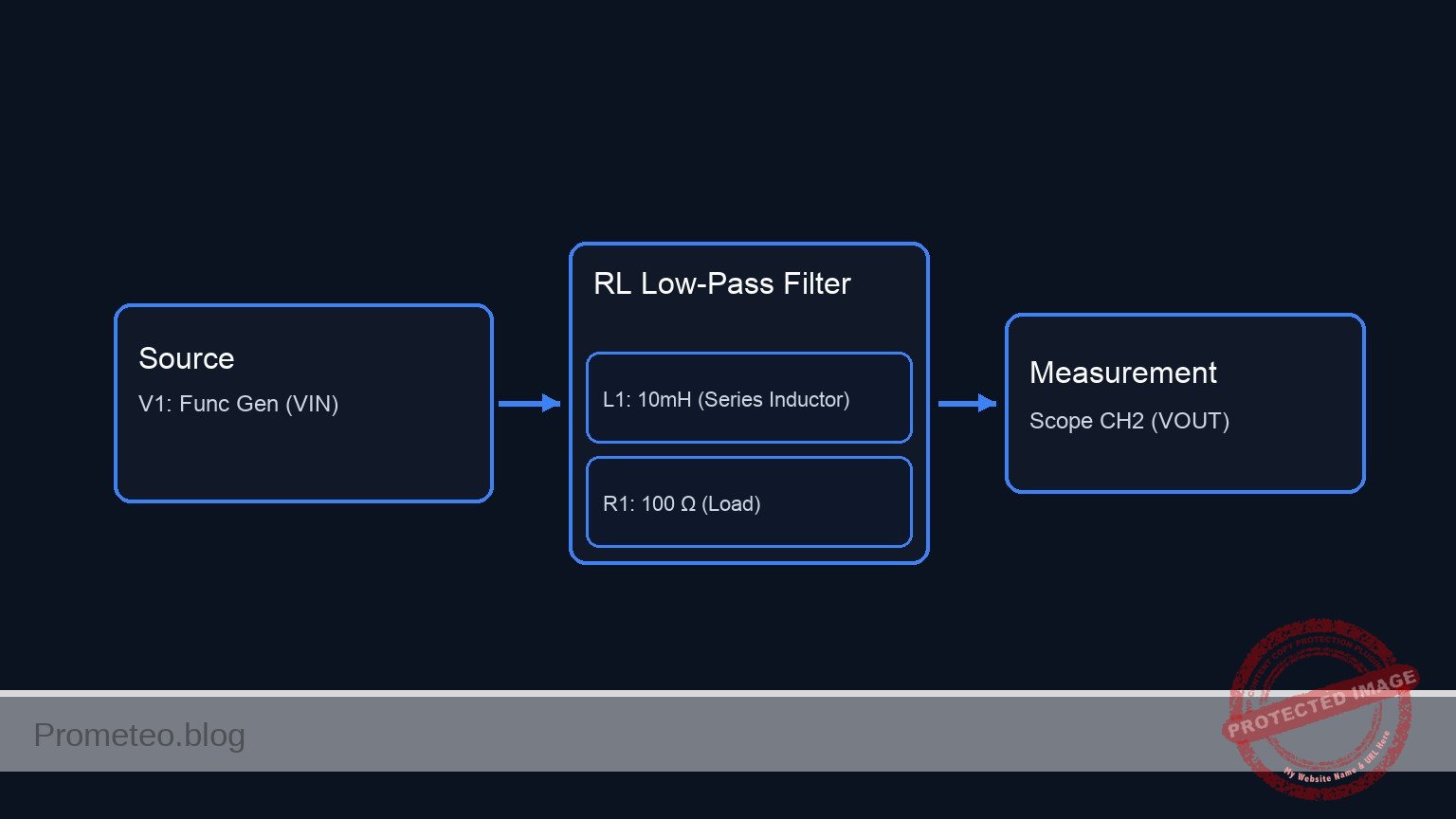
Conceptual block diagram

Conceptual block diagram — RL Low-Pass Filter
Quick read: inputs → main block → output (actuator or measurement). This summarizes the ASCII schematic below.

Schematic

[ V1: Func Gen ] --(Node VIN)--> [ L1: 10mH ] --(Node VOUT)--> [ R1: 100 Ω ] --> GND (0)
       |                        (Series Inductor)      |          (Load)
       |                                               |
       +--------(Probe)-------> [ Scope CH1 ]          +--------(Probe)-------> [ Scope CH2 ]
Schematic (ASCII)

Electrical diagram

Electrical diagram for case: Simple RL low-pass filter
Generated from the validated SPICE netlist for this case.

🔒 This electrical diagram is premium. With the monthly membership (7-day free trial) you can unlock the complete didactic material and the print-ready PDF pack.🔓 See premium access plans

Measurements and tests

Follow these steps to validate the frequency response of the filter.

  1. Setup: Configure the Function Generator (V1) to output a Sine Wave with 5 Vpp amplitude.
  2. Low Frequency Test (Pass Band):
    • Set V1 frequency to 100 Hz.
    • Observe Channel 1 (Input) and Channel 2 (Output) on the oscilloscope.
    • Result: The output wave (VOUT) should be almost identical in amplitude to the input (VIN).
  3. Cutoff Frequency Test (fc):
    • Calculate the theoretical cutoff: fc = (R / (2\pi L)) ≈ (100 / (2\pi × 0.01)) ≈ 1.59 kHz.
    • Set V1 frequency to 1.6 kHz.
    • Result: VOUT should be approximately 3.5 Vpp (roughly 0.707 × 5 Vpp). You will also notice a phase lag of -45°.
  4. High Frequency Test (Stop Band):
    • Set V1 frequency to 50 kHz.
    • Result: The output wave (VOUT) should be very small (highly attenuated) compared to the input.

SPICE netlist and simulation

Reference SPICE Netlist (ngspice) — excerptFull SPICE netlist (ngspice)

* Practical case: Simple RL Low-Pass Filter
.width out=256

* --- Component Definitions ---

* V1: Function Generator (Sine wave source)
* Wiring: Connects between node VIN (Positive) and node 0 (GND)
* Configuration: Sine wave, 0V offset, 5V amplitude, 2kHz frequency
* (Note: Cutoff frequency fc = R/(2*pi*L) approx 1.6kHz. 2kHz chosen to show attenuation)
V1 VIN 0 SIN(0 5 2k)

* L1: 10 mH inductor
* Wiring: Connects between node VIN and node VOUT
L1 VIN VOUT 10m

* R1: 100 Ohm resistor
* Wiring: Connects between node VOUT and node 0 (GND)
R1 VOUT 0 100

* --- Analysis Commands ---
* ... (truncated in public view) ...

Copy this content into a .cir file and run with ngspice.

🔒 Part of this section is premium. With the monthly membership (7-day free trial) you can access the full content (materials, wiring, detailed build, validation, troubleshooting, variants and checklist) and download the complete print-ready PDF pack.

* Practical case: Simple RL Low-Pass Filter
.width out=256

* --- Component Definitions ---

* V1: Function Generator (Sine wave source)
* Wiring: Connects between node VIN (Positive) and node 0 (GND)
* Configuration: Sine wave, 0V offset, 5V amplitude, 2kHz frequency
* (Note: Cutoff frequency fc = R/(2*pi*L) approx 1.6kHz. 2kHz chosen to show attenuation)
V1 VIN 0 SIN(0 5 2k)

* L1: 10 mH inductor
* Wiring: Connects between node VIN and node VOUT
L1 VIN VOUT 10m

* R1: 100 Ohm resistor
* Wiring: Connects between node VOUT and node 0 (GND)
R1 VOUT 0 100

* --- Analysis Commands ---

* Transient Analysis
* Step size: 1us
* Stop time: 2ms (sufficient to capture several cycles at 2kHz)
.tran 1u 2m

* Operating Point Analysis (DC check)
.op

* --- Output Directives ---

* Print Input (VIN) and Output (VOUT) voltages for simulation logging
* Scope Channel 1: VIN
* Scope Channel 2: VOUT
.print tran V(VIN) V(VOUT) I(L1)

.end

Simulation Results (Transient Analysis)

Simulation Results (Transient Analysis)

Analysis: The simulation shows a sinusoidal input (VIN) and a sinusoidal output (VOUT). At 2kHz, the output amplitude (approx 3V peak) is attenuated relative to the input (5V peak) and phase-shifted, consistent with RL low-pass filter behavior near its cutoff frequency.
Show raw data table (2012 rows)
Index   time            v(vin)          v(vout)         l1#branch
0	0.000000e+00	0.000000e+00	0.000000e+00	0.000000e+00
1	1.000000e-08	6.283185e-04	6.282557e-08	6.282557e-10
2	1.084006e-08	6.811008e-04	6.854662e-08	6.854662e-10
3	1.252017e-08	7.866654e-04	8.087543e-08	8.087543e-10
4	1.588039e-08	9.977945e-04	1.108531e-07	1.108531e-09
5	2.260084e-08	1.420053e-03	1.920880e-07	1.920880e-09
6	3.604174e-08	2.264569e-03	4.396687e-07	4.396687e-09
7	6.292353e-08	3.953601e-03	1.275216e-06	1.275216e-08
8	1.166871e-07	7.331665e-03	4.307397e-06	4.307397e-08
9	2.242143e-07	1.408778e-02	1.581244e-05	1.581244e-07
10	4.392686e-07	2.759992e-02	6.055593e-05	6.055593e-07
11	8.693773e-07	5.462350e-02	2.367416e-04	2.367416e-06
12	1.729595e-06	1.086651e-01	9.340244e-04	9.340244e-06
13	2.729595e-06	1.714719e-01	2.318447e-03	2.318447e-05
14	3.729595e-06	2.342516e-01	4.313902e-03	4.313902e-05
15	4.729595e-06	2.969943e-01	6.913992e-03	6.913992e-05
16	5.729595e-06	3.596901e-01	1.011228e-02	1.011228e-04
17	6.729595e-06	4.223291e-01	1.390231e-02	1.390231e-04
18	7.729595e-06	4.849014e-01	1.827756e-02	1.827756e-04
19	8.729595e-06	5.473972e-01	2.323151e-02	2.323151e-04
20	9.729595e-06	6.098065e-01	2.875758e-02	2.875758e-04
21	1.072959e-05	6.721195e-01	3.484918e-02	3.484918e-04
22	1.172959e-05	7.343264e-01	4.149966e-02	4.149966e-04
23	1.272959e-05	7.964173e-01	4.870237e-02	4.870237e-04
... (1988 more rows) ...


Reference SPICE netlist (ngspice)

* Practical case: Simple RL Low-Pass Filter
.width out=256

* --- Component Definitions ---

* V1: Function Generator (Sine wave source)
* Wiring: Connects between node VIN (Positive) and node 0 (GND)
* Configuration: Sine wave, 0V offset, 5V amplitude, 2kHz frequency
* (Note: Cutoff frequency fc = R/(2*pi*L) approx 1.6kHz. 2kHz chosen to show attenuation)
V1 VIN 0 SIN(0 5 2k)

* L1: 10 mH inductor
* Wiring: Connects between node VIN and node VOUT
L1 VIN VOUT 10m

* R1: 100 Ohm resistor
* Wiring: Connects between node VOUT and node 0 (GND)
R1 VOUT 0 100

* --- Analysis Commands ---

* Transient Analysis
* Step size: 1us
* Stop time: 2ms (sufficient to capture several cycles at 2kHz)
.tran 1u 2m

* Operating Point Analysis (DC check)
.op

* --- Output Directives ---

* Print Input (VIN) and Output (VOUT) voltages for simulation logging
* Scope Channel 1: VIN
* Scope Channel 2: VOUT
.print tran V(VIN) V(VOUT) I(L1)

.end

Simulation Results (Transient Analysis)

Simulation Results (Transient Analysis)

Analysis: The simulation shows a sinusoidal input (VIN) and a sinusoidal output (VOUT). At 2kHz, the output amplitude (approx 3V peak) is attenuated relative to the input (5V peak) and phase-shifted, consistent with RL low-pass filter behavior near its cutoff frequency.

Common mistakes and how to avoid them

  1. Measuring across the Inductor: If you measure voltage across L1 instead of R1, you create a High-Pass filter (passing high frequencies). Solution: Ensure the oscilloscope probe monitors the node between L1 and R1 relative to Ground.
  2. Using DC Input: An inductor acts as a short circuit in DC (after the transient). Solution: Ensure the function generator is set to AC (Sine Wave) to observe reactance effects.
  3. Inductor Saturation: Using a very small inductor core with high current can saturate the magnetic field, distorting the waveform. Solution: Use an appropriate inductor or keep signal current within the component’s rating.

Troubleshooting

  • Symptom: VOUT is zero at all frequencies.
    • Cause: Open circuit in the wiring or broken inductor wire.
    • Fix: Check continuity of L1 and connections at VIN and VOUT.
  • Symptom: VOUT equals VIN at all frequencies.
    • Cause: The inductor L1 is shorted or R1 is disconnected (open).
    • Fix: Measure the resistance of L1 (should be non-zero but low) and ensure R1 is properly grounded.
  • Symptom: No attenuation observed at 50 kHz.
    • Cause: Inductor value is too small or Resistor value is too large (cutoff frequency is too high).
    • Fix: Verify component values. Try increasing L1 or decreasing R1 to lower the cutoff frequency.

Possible improvements and extensions

  1. Bode Plotting: Manually record the amplitude of VOUT at 10 different frequencies from 100 Hz to 100 kHz and plot the results on semi-log graph paper to visualize the -20dB/decade roll-off.
  2. Second Order Filter: Add a capacitor in parallel with R1 to create an RLC low-pass filter, creating a steeper roll-off (-40dB/decade) and potentially introducing resonance.

More Practical Cases on Prometeo.blog

Find this product and/or books on this topic on Amazon

Go to Amazon

As an Amazon Associate, I earn from qualifying purchases. If you buy through this link, you help keep this project running.

Quick Quiz

Question 1: What type of filter is described in this practical exercise?


Question 2: Which component acts as the series reactive element in this circuit?


Question 3: How does the impedance of an inductor change with frequency?


Question 4: Where is the output voltage typically measured in a series RL low-pass filter configuration?


Question 5: What happens to the output amplitude when the input frequency is significantly higher than the cutoff frequency?


Question 6: In audio electronics, what is a common use for this type of filter?


Question 7: Why is this circuit useful in power supplies?


Question 8: What is the primary function of the inductor in this circuit regarding signal frequencies?


Question 9: Which application involves removing high-frequency noise from sensor data?


Question 10: What is the expected outcome for a Low Frequency Input (< Cutoff) in this circuit?


Carlos Núñez Zorrilla
Electronics & Computer Engineer

Telecommunications Electronics Engineer and Computer Engineer (official degrees in Spain).

Follow me: